EP1298443B1 - Circuit and method for adjusting the clock skew in a communications system - Google Patents
Circuit and method for adjusting the clock skew in a communications system Download PDFInfo
- Publication number
- EP1298443B1 EP1298443B1 EP02016652A EP02016652A EP1298443B1 EP 1298443 B1 EP1298443 B1 EP 1298443B1 EP 02016652 A EP02016652 A EP 02016652A EP 02016652 A EP02016652 A EP 02016652A EP 1298443 B1 EP1298443 B1 EP 1298443B1
- Authority
- EP
- European Patent Office
- Prior art keywords
- data
- input
- clock
- clock skew
- circuit
- Prior art date
- Legal status (The legal status is an assumption and is not a legal conclusion. Google has not performed a legal analysis and makes no representation as to the accuracy of the status listed.)
- Expired - Fee Related
Links
Images

Classifications
-
- G—PHYSICS
- G01—MEASURING; TESTING
- G01R—MEASURING ELECTRIC VARIABLES; MEASURING MAGNETIC VARIABLES
- G01R31/00—Arrangements for testing electric properties; Arrangements for locating electric faults; Arrangements for electrical testing characterised by what is being tested not provided for elsewhere
- G01R31/28—Testing of electronic circuits, e.g. by signal tracer
- G01R31/317—Testing of digital circuits
- G01R31/31725—Timing aspects, e.g. clock distribution, skew, propagation delay
-
- G—PHYSICS
- G01—MEASURING; TESTING
- G01R—MEASURING ELECTRIC VARIABLES; MEASURING MAGNETIC VARIABLES
- G01R31/00—Arrangements for testing electric properties; Arrangements for locating electric faults; Arrangements for electrical testing characterised by what is being tested not provided for elsewhere
- G01R31/28—Testing of electronic circuits, e.g. by signal tracer
- G01R31/317—Testing of digital circuits
- G01R31/3181—Functional testing
- G01R31/319—Tester hardware, i.e. output processing circuits
- G01R31/31903—Tester hardware, i.e. output processing circuits tester configuration
- G01R31/31908—Tester set-up, e.g. configuring the tester to the device under test [DUT], down loading test patterns
- G01R31/3191—Calibration
-
- G—PHYSICS
- G01—MEASURING; TESTING
- G01R—MEASURING ELECTRIC VARIABLES; MEASURING MAGNETIC VARIABLES
- G01R31/00—Arrangements for testing electric properties; Arrangements for locating electric faults; Arrangements for electrical testing characterised by what is being tested not provided for elsewhere
- G01R31/28—Testing of electronic circuits, e.g. by signal tracer
- G01R31/317—Testing of digital circuits
- G01R31/3181—Functional testing
- G01R31/319—Tester hardware, i.e. output processing circuits
- G01R31/3193—Tester hardware, i.e. output processing circuits with comparison between actual response and known fault free response
- G01R31/31937—Timing aspects, e.g. measuring propagation delay
Definitions
- delays in digital communications systems are oftentimes longer than delays in traditional designs. For instance, delays in some digital communications systems are multiple clock periods in length. The delays in digital communications systems are oftentimes longer than delays in traditional designs because some data processing tasks require more than one clock period to execute. In addition, the delays are oftentimes longer than delays in traditional designs because the physical length of transmission lines connecting system components together are longer than transmission lines utilized in traditional designs. As can be understood, the longer delays can complicate data transfer between components in a system.
- a prior attempt to work around the shortcomings of the above-described oscilloscope-based system involves measuring the bit error rate (BER) of the data output generated by the system component under test as the clock skew is varied, and choosing the clock skew having the lowest BER.
- BER bit error rate
- this approach is problematical because there are usually a number of cascaded system components involved in a BER test, all of which have to have the correct clock skew in order to obtain correct data at the output of the chain of cascaded components.
- This approach of measuring the BER of a system therefore, requires a multi-dimensional search to arrive at a usable set of clock skews.
- the relationship between BER and clock skew is such that identifying a minimum BER is often difficult.
- Exemplary circuitry for effectuating the clock skew adjusting and shifting includes phase shifter circuitry connected to a clock input of one of the device under test and the data source, and a voltage measuring circuit connected to the output of the device under test.
- circuit 1 includes a bias circuit 4 connected between a data output of a data source 5 and a data input of device 2A.
- Bias circuit 4 commonly referred to as a level shifter, includes a first input for receiving an input signal, such as a signal having little or no DC offset, a second input for receiving a DC bias, and an output.
- Bias circuit 4 combines the DC bias appearing at its second input to the signal appearing at the first input to obtain a combined signal, and applies the combined signal to the output of bias circuit 4. In this way, bias circuit 4 is used to vary the DC offset of the data signal applied to the device 2A.
- device 2B may internally add a DC bias to a digital signal generated by device 2B. In this instance, bias circuit 4 would be unnecessary.
- circuit 1 includes a phase shift circuit 7 connected between a system clock 11 of system 3 and the clock input of device 2A.
- Phase shift circuit 7 includes a clock input and a control input. The output signal generated by phase shift circuit 7 is shifted in phase relative to the clock input thereof by an amount based upon the control input.
- the clock skew between the input clocks for device 2B and device 2A may be set to the desired amount.
- a voltmeter 8 is connected to the output of device 2A via a splitter circuit 6. Voltmeter 8 measures and visually indicates the DC voltage appearing at the output of device 2A. Splitter circuit 6 allows voltmeter 8 to measure the DC level appearing in the output of device 2A.
- the operation of the present invention to optimize the clock skew between device 2B and device 2A in system 3 is, in general terms, a two step operation. First, the clock skew between device 2A and device 2B is adjusted to approximately 180 degrees. Second, the 180 degree clock skew is then shifted by approximately 180 degrees so as to set the clock skew between devices 2A and 2B to approximately zero degrees.
- a DC offset added to the input data pattern applied to device 2A can be used to determine when the clock skew between devices 2A and 2B is 180 degrees.
- data source 5 provides an input data pattern to device 2A having a particular duty cycle, i.e., a particular ratio of logic one data bits to logic zero data bits. If the clock skew between the clock input of device 2A and the clock input of data source 5 is optimized (i.e., at a clock skew such that input data to device 2A is interpreted without error), the output of device 2A will have the same duty cycle as the input data pattern. The DC component of the output of device 2A will therefore correspond to the particular duty cycle of the input data pattern provided to device 2A.
- device 2A will ideally make random decisions at each triggering edge of the clock input to device 2A.
- the random decisions are whether to interpret the input data pattern as the outgoing data bits (already maintained by device 2A) or the incoming data bits (appearing at the data input of device 2A).
- the duty cycle of the output data pattern generated by device 2A will ideally be the same as the duty cycle of the input data pattern applied to device 2A. From this it can be seen that for a clock skew of 180 degrees between devices 2A and 2B, the DC component of the data pattern appearing at the output of device 2A will closely correspond to the duty cycle of the input data pattern applied to device 2A.
- a DC offset in the direction of a logic zero value will increase the likelihood that logic zero data bits will be interpreted by device 2A. Most of the input data bits of the input data pattern that transition will be interpreted as a logic zero data bit. The increase in logic zero data bit interpretation decreases the duty cycle of the data output pattern generated by device 2A to approximately 0% and thereby decreases the DC component of the data output pattern generated by device 2A.
- the duty cycle of the output data pattern generated by device 2A will be between 0% and 50%.
- the resulting DC bias in the output data pattern will therefore be less in magnitude at clock skew amounts close to 180 degrees than the DC bias in the output data pattern at a 180 degree clock skew.
- clock skew amounts close to 180 degrees, the transfer of DC offset from the data input to device 2A to the data output thereof is therefore less than the transfer of DC offset at a 180 degree clock skew.
- FIG. 2 A curve illustrating the relationship between clock skew and the transfer of DC offset from the data input of device 2A to the data output thereof is shown in Fig. 2.
- the curve of Fig. 2 describes the DC offset transfer characteristic of device 2A over a range of clock skew values. It is understood that the shape of the curve of Fig. 2 may depend in part upon the characteristics of the particular hardware in system 3.
- bias circuit 4 is manipulated at 31 so that a predetermined DC offset is added to the data provided to the data input of device 2A.
- the magnitude of the predetermined DC offset is selected to be large enough so that a measurable DC offset level may be transferred from the data input of device 2A to the data output thereof, and small enough so that transferred DC offset peaks at the 180 clock skew instead of the peak being broadened so as to make the peak relatively indistinguishable.
- the data pattern is applied to device 2A at 32.
- the data pattern may be a repeated data pattern so that data is substantially continuously provided to device 2A during the operation to optimize the clock skew.
- phase shift circuit 7 in Fig. 1 provides a clock skew between the clock input to device 2A and the clock input to data source 5 (i.e., the system clock 11), phase shift circuit 7 may be located elsewhere in circuit 1 while still allowing a clock skew between device 2A and data source 5.
- Fig. 4 illustrates a circuit 10 according to another exemplary embodiment of the present invention.
- the phase shift circuit 7 of circuit 10 is disposed between the system clock 11 and the clock input to data source 5.
- the system clock 11 is in this embodiment directly connected to the clock input of device 2A.
- Circuit 10 may be employed to set the clock skew between the clock input of device 2A and the clock input of data source 5 to the optimum value.
- the operation for setting the clock skew to the optimum value is substantially the same as the operation described above with respect to circuit 1 of Fig. 1.
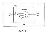
- Fig. 6 illustrates a device under test 15 having a plurality of data inputs.
- the desired clock skew between the clock input to device 15 and the clock input to the data source may be obtained by setting all but one of the data inputs to device 15 to a static or constant logic level and applying a data pattern to one data input.
- the timing of the various data sources providing data to device 15 may be adjusted to the desired or optimum setting.
- device 15 is illustrated as a multiplexer circuit for exemplary purposes only. It is understood that device 15 may be virtually any clocked, multiple-input device.
Description
- The present invention relates to adjusting the timing within a communications system, and particularly to adjusting the clock timing between devices within the communications system.
- US 6,239,629 relates to a signal comparison system which determines whether a data signal is transitioning close to transitions of its clock signal, thereby causing possible errors in the sampling of the data signal. The signal comparison system includes a plurality of latches that receive a first signal and a second signal and that transmit a respective value of the first signal in response to a transition of the second signal. A delay mechanism delays the transition of the second signal before the transition is received by latches so that the transition is delayed different amounts relative to each of the latches. A feedback mechanism receives the values transmitted by the latches and determines whether these values are logically equivalent. The feedback mechanism then transmits a feedback signal in response to a determination that one of the values is logically different than another of the values.
- US 4,550,405 relates to an electric pulse edge timing adjustment circuit comprising one or more deskew elements. In each deskew element, a pulse train is passed through an inverter. The falling rate of pulse edges on the inverter output line is controlled by a capacitor and an adjustable current sink which determine the output line capacitance discharge rate. From the output line, pulses are passed to another deskew element which re-inverts the pulses and delays the formerly rising pulse edges. Each current sink is independently adjustable to allow different delays in the rising and falling edges.
- US 5,856,753 relates to an analog based pre-driver and pad as well as a duty cycle adjustment cell prior to the pre-driver and pad. The pre-driver and pad may operate in either a 3 volt mode, a 5 volt mode or any voltage in between depending only on the power supply voltage present. No production configuration or post-production configuration is required. The patent discloses a special bias circuit to reduce the Vcc, temperature and other processing variations. A duty cycle cell produces a range of duty cycles when the circuit is operating between a 3 volt and 5 volt range.
- Traditionally, synchronously clocked logic systems utilize a timing methodology requiring all logic elements to be clocked simultaneously, or at least with tolerable clock skew. This methodology is suitable for computers in which the entire central processing unit is disposed in a single integrated circuit so that delays can be well controlled. However, this methodology proves ineffective in the case of digital communications systems operating at higher speeds, such as ethernet and fiber optic data links. In these systems, data often flows through various data processing components in a somewhat asynchronous fashion. Typical data communication components in these systems include multiplexers/demultiplexers (also known as serializers/deserializers), error correction processors, and protocol/format converters. In some digital communications systems, there are many clocks having various phases relative to each other, and in many cases the clocks operate at different integer multiples of a clock frequency.
- In addition, delays in digital communications systems are oftentimes longer than delays in traditional designs. For instance, delays in some digital communications systems are multiple clock periods in length. The delays in digital communications systems are oftentimes longer than delays in traditional designs because some data processing tasks require more than one clock period to execute. In addition, the delays are oftentimes longer than delays in traditional designs because the physical length of transmission lines connecting system components together are longer than transmission lines utilized in traditional designs. As can be understood, the longer delays can complicate data transfer between components in a system.
- Further complicating data transfer between system components in digital communications systems is the fact that many system components generate internal clocks that are phase locked to an externally available clock and have indeterminate phase shifts, relative to the externally available clock. There is often no particular timing relationship between the time when the input data to a system component is sampled, when the output data of the component transitions, and the occurrence of the triggering edge of the internal clock(s). As a result, a need exists for adjusting the timing within systems, such as digital communications systems, so that data is sampled by the system components at the appropriate time.
- Efforts to better control the timing between components in a system have met with limited success. Some systems and test equipment apply a repetitive test pattern to a system component while the output of the system component is observed with a high-speed sampling oscilloscope. During this time, the phase of the clock input to the system component can be manually adjusted until the system component under test produces the correct output data, based on the data going into the component. The oscilloscope is capable of effectively sampling at many different clock phases so that usually there is no problem synchronizing the oscilloscope to the output data. However, there are two serious limitations to employment of an oscilloscope in this manner. First, the oscilloscope limits the maximum data rate of the system to be the maximum speed observable on the fastest available oscilloscope. Second, in a system to be used outside the laboratory, it is not economically feasible to build an expensive oscilloscope into the system for the purpose of adjusting clock skew in the field.
- A prior attempt to work around the shortcomings of the above-described oscilloscope-based system involves measuring the bit error rate (BER) of the data output generated by the system component under test as the clock skew is varied, and choosing the clock skew having the lowest BER. However, this approach is problematical because there are usually a number of cascaded system components involved in a BER test, all of which have to have the correct clock skew in order to obtain correct data at the output of the chain of cascaded components. This approach of measuring the BER of a system, therefore, requires a multi-dimensional search to arrive at a usable set of clock skews. In addition, the relationship between BER and clock skew is such that identifying a minimum BER is often difficult.
- Based upon the foregoing, there is a need for a simple and accurate method for adjusting clock skew or other timing within a communications system.
- The present invention provides a method for adjusting clock signals according to
claim 1 and a circuit for adjusting clock signals according toclaim 5. - Embodiments of the present invention overcome shortcomings in prior techniques for adjusting timing and satisfy a significant need for a method and device for relatively quickly and accurately adjusting clock signals for devices in a system. Clock skew and/or phase between the clock input to a device under test and a clock input to a data source is first adjusted to approximately 180 degrees. Thereafter, the 180 degree clock skew is shifted by approximately 180 degrees to obtain near zero clock skew. In particular, the clock skew is adjusted to approximately 180 degrees by applying an input data pattern to the device under test having a predetermined DC offset voltage, and measuring a DC offset voltage of the output of the device under test at a plurality of different clock skew amounts. The clock skew that produces the largest magnitude of DC offset at the data output of the device under test is the clock skew of 180 degrees.
- Exemplary circuitry for effectuating the clock skew adjusting and shifting includes phase shifter circuitry connected to a clock input of one of the device under test and the data source, and a voltage measuring circuit connected to the output of the device under test.
- Furthermore, the invention provides embodiments with other features and advantages in addition to or in lieu of those discussed above. Many of these features and advantages are apparent from the description below with reference to the following drawings.
- A more complete understanding of the method and apparatus of the present invention may be obtained by reference to the following Detailed Description when taken in conjunction with the accompanying Drawings wherein:
- Fig. 1 is a block diagram of a portion of a communications system according to an exemplary embodiment of the present invention;
- Fig. 2 is a graph of a DC offset transfer curve corresponding to the portion of the communications system of Fig. 1;
- Fig. 3 is a flow chart illustrating an operation of the portion of the communications system of Fig. 1;
- Fig. 4 is a block diagram of a portion of a communications system according to another exemplary embodiment of the present invention;
- Fig. 5 is a block diagram of a portion of a communications system according to yet another exemplary embodiment of the present invention; and
- Fig. 6 is a diagram of a multiple-input device under test according to another exemplary embodiment of the present invention.
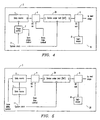
- Referring to Fig. 1, there is shown a
circuit 1 for adjusting clock skew betweendevices system 3, such as a communications system, according to an exemplary embodiment of the present invention.Circuit 1 allows clock inputs todevices system 3 to be precisely set relative to each other so that the clock skew between the clock inputs todevices - It is understood that
devices synchronous system 3. It is understood thatsystem 3 may be any system in which clock timing is relatively difficult to tightly control. For reasons of simplicity, eachdevice - With reference to the portion of
system 3 shown in Fig. 1,device 2A under test receives data fromdevice 2B, and particularly from adata source 5 ofdevice 2B. According to an exemplary embodiment of the present invention,circuit 1 includes abias circuit 4 connected between a data output of adata source 5 and a data input ofdevice 2A.Bias circuit 4, commonly referred to as a level shifter, includes a first input for receiving an input signal, such as a signal having little or no DC offset, a second input for receiving a DC bias, and an output.Bias circuit 4 combines the DC bias appearing at its second input to the signal appearing at the first input to obtain a combined signal, and applies the combined signal to the output ofbias circuit 4. In this way,bias circuit 4 is used to vary the DC offset of the data signal applied to thedevice 2A. - It is understood that
device 2B may internally add a DC bias to a digital signal generated bydevice 2B. In this instance,bias circuit 4 would be unnecessary. - Systems conventionally include a common clock signal, such as a system clock, that is directly connected to the clock input of each system device in the system. According to the exemplary embodiment of the present invention illustrated in Fig. 1, however,
circuit 1 includes aphase shift circuit 7 connected between asystem clock 11 ofsystem 3 and the clock input ofdevice 2A.Phase shift circuit 7 includes a clock input and a control input. The output signal generated byphase shift circuit 7 is shifted in phase relative to the clock input thereof by an amount based upon the control input. Withdata source 5 being directly connected to thesystem clock 11 anddevice 2A being connected to thesystem clock 11 viaphase shift circuit 7, the clock skew between the input clocks fordevice 2B anddevice 2A may be set to the desired amount. - A
voltmeter 8 is connected to the output ofdevice 2A via asplitter circuit 6.Voltmeter 8 measures and visually indicates the DC voltage appearing at the output ofdevice 2A.Splitter circuit 6 allowsvoltmeter 8 to measure the DC level appearing in the output ofdevice 2A. - The operation of the present invention to optimize the clock skew between
device 2B anddevice 2A insystem 3 is, in general terms, a two step operation. First, the clock skew betweendevice 2A anddevice 2B is adjusted to approximately 180 degrees. Second, the 180 degree clock skew is then shifted by approximately 180 degrees so as to set the clock skew betweendevices - The rationale behind the operation is as follows. A DC offset added to the input data pattern applied to
device 2A can be used to determine when the clock skew betweendevices data source 5 provides an input data pattern todevice 2A having a particular duty cycle, i.e., a particular ratio of logic one data bits to logic zero data bits. If the clock skew between the clock input ofdevice 2A and the clock input ofdata source 5 is optimized (i.e., at a clock skew such that input data todevice 2A is interpreted without error), the output ofdevice 2A will have the same duty cycle as the input data pattern. The DC component of the output ofdevice 2A will therefore correspond to the particular duty cycle of the input data pattern provided todevice 2A. - If the clock skew between
devices device 2A will not affect the ability ofdevice 2A to correctly interpret the input data pattern.Device 2A will still be able to interpret the input data pattern with sufficient margin. The duty cycle of the output data pattern generated bydevice 2A will therefore be the same as the duty cycle of the input data pattern applied todevice 2A. As a result, a DC offset added to the input data pattern will not change the DC component of the data output pattern. There is thus little or no transfer of DC offset from the input data pattern applied todevice 2A to the output data pattern generated thereby at relatively small clock skew amounts. - If the clock skew between
devices device 2A will ideally make random decisions at each triggering edge of the clock input todevice 2A. The random decisions are whether to interpret the input data pattern as the outgoing data bits (already maintained bydevice 2A) or the incoming data bits (appearing at the data input ofdevice 2A). Without any other conditions effecting the timing or signal levels of the data and clock inputs todevice 2A, there is an equal probability of a logic zero data bit being interpreted as a logic one data bit as there is a logic one data bit being interpreted as a logic zero data bit. As a result, the duty cycle of the output data pattern generated bydevice 2A will ideally be the same as the duty cycle of the input data pattern applied todevice 2A. From this it can be seen that for a clock skew of 180 degrees betweendevices device 2A will closely correspond to the duty cycle of the input data pattern applied todevice 2A. - However, if a DC offset is added to the input data pattern applied to
device 2A while the clock skew remains at 180 degrees, the decisions made bydevice 2A will change. The probability ofdevice 2A interpreting a logic zero data bit will no longer be the same as the probability ofdevice 2A interpreting a logic one data bit. For instance, a DC offset added to the input data pattern in the direction of a logic one value will increase the likelihood thatdevice 2A will interpret logic one data bits. Most of the input data bits of the input data pattern that transition will be interpreted as a logic one data bit. This increased likelihood of a logic one data bit interpretation increases the duty cycle of the data output pattern generated bydevice 2A to approximately 100% and thereby increases the DC component of the data output pattern. - Similarly, a DC offset in the direction of a logic zero value will increase the likelihood that logic zero data bits will be interpreted by
device 2A. Most of the input data bits of the input data pattern that transition will be interpreted as a logic zero data bit. The increase in logic zero data bit interpretation decreases the duty cycle of the data output pattern generated bydevice 2A to approximately 0% and thereby decreases the DC component of the data output pattern generated bydevice 2A. - From this it can be seen that at a clock skew of 180 degrees, the DC offset in the input data pattern applied to
device 2A causes a change in the DC offset in the output data pattern generated bydevice 2A. In other words, there is a relatively sizeable transfer of DC offset from the input data pattern applied todevice 2A to the output data pattern generated thereby when the clock skew betweendevice 2A anddata source 5 is at 180 degrees. - For clock skew values close to but not equaling 180 degree, such as clock skews between 160 degrees and 180 degrees, a DC offset added to the input data pattern of
device 2A affects the DC offset in the output data pattern ofdevice 2A. However, the effect is less than when the clock skew is at 180 degrees. At clock skew values close to 180 degrees, noise and jitter will cause a statistical distribution of the output data pattern generated bydevice 2A to change the duty cycle of the output data pattern, relative to the duty cycle of the output data pattern at a 180 degree clock skew. In the event the input data pattern has a DC bias in the direction of a logic one and a 50% duty cycle, the duty cycle of the output data pattern generated bydevice 2A will be between 50% and 100%. In the event the input data pattern has a DC bias in the direction of a logic zero and a 50% duty cycle, the duty cycle of the output data pattern generated bydevice 2A will be between 0% and 50%. The resulting DC bias in the output data pattern will therefore be less in magnitude at clock skew amounts close to 180 degrees than the DC bias in the output data pattern at a 180 degree clock skew. At clock skew amounts close to 180 degrees, the transfer of DC offset from the data input todevice 2A to the data output thereof is therefore less than the transfer of DC offset at a 180 degree clock skew. - A curve illustrating the relationship between clock skew and the transfer of DC offset from the data input of
device 2A to the data output thereof is shown in Fig. 2. The curve of Fig. 2 describes the DC offset transfer characteristic ofdevice 2A over a range of clock skew values. It is understood that the shape of the curve of Fig. 2 may depend in part upon the characteristics of the particular hardware insystem 3. - The magnitude of the DC offset added to the input data pattern to
device 2A affects the shape of the curve of Fig. 2. Specifically, increasing the magnitude of the DC offset of the input data pattern applied todevice 2A broadens the curve of Fig. 2, and decreasing the magnitude of the DC offset of the input data pattern narrows the curve. Fig. 2 shows the relationship between clock skew and the transfer of DC offset at a first DC offset value (in solid lines) and a second DC offset value that is of a smaller magnitude relative to the first DC offset value (in dashed lines). - Based upon the relationship between clock skew and the transfer of DC offset from the data input of
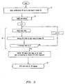
device 2A to the data output thereof, the operation ofcircuit 1 to optimize clock skew betweendevice 2A anddata source 5 will be described with reference to Fig. 3. First,bias circuit 4 is manipulated at 31 so that a predetermined DC offset is added to the data provided to the data input ofdevice 2A. The magnitude of the predetermined DC offset is selected to be large enough so that a measurable DC offset level may be transferred from the data input ofdevice 2A to the data output thereof, and small enough so that transferred DC offset peaks at the 180 clock skew instead of the peak being broadened so as to make the peak relatively indistinguishable. - Next, a data pattern is applied to
device 2A at 32. The data pattern may be a repeated data pattern so that data is substantially continuously provided todevice 2A during the operation to optimize the clock skew. - The clock skew between
data source 5 anddevice 2A is then adjusted at 33 to approximately 180 degrees. The clock skew adjustment is accomplished by manipulatingphase shift circuit 7 to present a clock skew between the clock input ofdevice 2A and the clock input ofdata source 5 and reading, usingvoltmeter 8, the DC offset in the data output generated bydevice 2A. The manipulating and reading is then repeated a number of times with other clock skew amounts. Repeating the manipulating and reading steps result in the identification of a number of locations along the DC offset voltage-versus-clock phase function shown in Fig. 2. The clock skew setting yielding the DC offset voltage in the data output ofdevice 2A having the greatest magnitude is identified as the 180 degree clock skew. The 180 degree clock skew yields the largest magnitude DC offset in the data output due to the relationship between clock skew and the transfer of DC offset as illustrated in Fig. 2. - Next, the 180 degree clock skew is then shifted at 34 by approximately 180 degrees so as to set the clock skew between
data source 5 anddevice 2A to be approximately zero degrees. The 180 degree clock skew is shifted by manipulatingphase shift circuit 7. The procedure for shifting the clock skew varies based upon the characteristics ofphase shift circuit 7. In the eventphase shift circuit 7 is calibrated in terms of phase shift versus control voltage, a calibration table may be referred to in order to implement the 180 degree phase shift. Alternatively, in the eventphase shift circuit 7 is linear but of unknown gain, the gain can be determined by finding two adjacent clock skew settings, such as 180 degrees and -180 degrees. The two adjacent clock skew settings may be obtained by using, for example, steps 31-33 described above for each adjacent clock skew setting. Because the two adjacent clock skew settings are approximately 360 degrees apart, the optimum clock skew setting (i.e., the clock skew setting resulting in input data todevice 2A being interpreted without error) is the midpoint between the adjacent clock skew settings. - It is understood that the clock skew may be shifted in
step 34 by an amount other than 180 degrees to obtain a desired clock skew amount other than a zero degree clock skew. - It is understood that since
phase shift circuit 7 in Fig. 1 provides a clock skew between the clock input todevice 2A and the clock input to data source 5 (i.e., the system clock 11),phase shift circuit 7 may be located elsewhere incircuit 1 while still allowing a clock skew betweendevice 2A anddata source 5. Fig. 4 illustrates acircuit 10 according to another exemplary embodiment of the present invention. Thephase shift circuit 7 ofcircuit 10 is disposed between thesystem clock 11 and the clock input todata source 5. Thesystem clock 11 is in this embodiment directly connected to the clock input ofdevice 2A. Circuit 10 may be employed to set the clock skew between the clock input ofdevice 2A and the clock input ofdata source 5 to the optimum value. The operation for setting the clock skew to the optimum value is substantially the same as the operation described above with respect tocircuit 1 of Fig. 1. - Fig. 5 illustrates a
circuit 20 according to yet another exemplary embodiment of the present invention. Instead of using aphase shift circuit 7 to arrive at an optimum clock skew between the clock inputs ofdevice 2A anddata source 5, avariable delay circuit 9 is disposed between the data output ofdata source 5 and the data input ofbias circuit 4. Thesystem clock 11 is directly connected to the clock inputs ofdevice 2A anddata source 5.Variable delay circuit 9 may be controlled to vary the delay between the data input ofvariable delay circuit 9 and the data output thereof. By altering the delay of the data betweendata source 5 anddevice 2A, differences in clock delays betweendata source 5 anddevice 2A may be corrected and optimized. The clock delay is effectively optimized by following steps 31-34 above, with the understanding thatvariable delay circuit 9 is manipulated to adjust the effective clock skew setting to approximately 180 degrees and to shift the 180 degree clock skew setting by approximately 180 degrees thereafter. - It is understood that embodiments of the present invention may be used to optimize the clock timing between multiple-input devices in a system. Fig. 6 illustrates a device under
test 15 having a plurality of data inputs. In the event that the data inputs todevice 15 have similar timing, the desired clock skew between the clock input todevice 15 and the clock input to the data source may be obtained by setting all but one of the data inputs todevice 15 to a static or constant logic level and applying a data pattern to one data input. In the event the data inputs todevice 15 do not have similar timing, the timing of the various data sources providing data todevice 15 may be adjusted to the desired or optimum setting. - In Fig. 6,
device 15 is illustrated as a multiplexer circuit for exemplary purposes only. It is understood thatdevice 15 may be virtually any clocked, multiple-input device. - Although various embodiments of the method, system, and apparatus of the present invention have been illustrated in the accompanying Drawings and described in the foregoing Detailed Description, it will be understood that the invention is not limited to the embodiments disclosed, but is capable of numerous rearrangements, modifications and substitutions without departing from the scope of the invention as set forth and defined by the following claims.
Claims (10)
- A method for adjusting clock signals for a device (2A) in a system (3), comprising:adjusting to approximately 180 degrees a clock skew between a clock input to the device (2A) and a clock input to a data source (5) providing data to the device (2A) to obtain an 180 degree clock skew;adding a DC offset to the data provided by the data source (5); andshifting by approximately 180 degrees the 180 degree clock skew.
- The method of claim 1, wherein:the step of adjusting comprises adjusting the clock skew between the device (2A) to two separate clock skew amounts of approximately +180 degrees and -180 degrees; andthe step of shifting comprises shifting the clock skew from one of the two separate clock skew amounts to a clock skew amount approximately at a midpoint between the two separate clock skew amounts.
- The method of claim 1, wherein the step of adjusting comprising:initially setting the DC offset of at least one data input of the device (2A) to a predetermined level;adjusting the clock skew between the clock input to the device (2A) and the clock input to the data source (5) to approximately 180 degrees;applying a data pattern to the at least one data input of the device (2A);varying the clock skew;monitoring a data output of the device (2A); andidentifying the 180 degree clock skew as the clock skew corresponding to a maximum DC offset appearing at the output of the device (2A).
- The method of claim 1, wherein the step of adjusting comprises:initially setting a DC offset of at least one data input of the device (2A) to an initial level; anddetermining a clock skew amount resulting in a maximum DC offset in a data output of the device (2A), the clock skew amount comprising the 180 degree clock skew.
- A circuit (1) for adjusting clock signals for a device (2A) in a system (3) comprising:a first circuit (7; 9) for selectively adjusting a clock skew between a clock input to the device (2A) and a clock input to a data source (5) providing data to a data input of the device (2A);a second circuit (4) connected to a data input of the device (2A) for providing a DC offset to signals appearing at the data input of the device (2A); anda third circuit (6) coupled to a data output of the device (2A) for measuring a DC offset of the data output of the device (2A).
- The circuit of claim 5, wherein :the first circuit (7; 9) selectively adjusts a delay between the clock input to the device (2A) and an output of the data source (5) providing data to the device (2A).
- The circuit (1) of claim 6, wherein:the first circuit comprises a delay circuit (9) having a first input connected to a data output of the data source (5) and an output coupled to the first input of the device (2A) and capable of providing any of a plurality of delays between a signal appearing at the input of the delay circuit (9) and a signal appearing at the output thereof.
- The circuit (1) of claim 5 or 6, wherein:the first input of the device (2A) is a data input; andthe first output of the data source (5) is a data output.
- The circuit (1) of claim 5, 6, 7 or 8, wherein:the second circuit (4) comprises a circuit capable of providing a DC offset to the first input of the device (2A) having any of a plurality of DC values.
- The circuit (1) of any of claims 5 to 9, wherein the third circuit comprises:a signal splitter circuit (6) having an input connected to a data output of the device (2A) and an output capable of providing a signal representative of a DC offset of the data output of the device (2A).
Applications Claiming Priority (2)
| Application Number | Priority Date | Filing Date | Title |
|---|---|---|---|
| US09/967,443 US6823466B2 (en) | 2001-09-28 | 2001-09-28 | Circuit and method for adjusting the clock skew in a communications system |
| US967443 | 2001-09-28 |
Publications (3)
| Publication Number | Publication Date |
|---|---|
| EP1298443A2 EP1298443A2 (en) | 2003-04-02 |
| EP1298443A3 EP1298443A3 (en) | 2004-06-16 |
| EP1298443B1 true EP1298443B1 (en) | 2005-09-21 |
Family
ID=25512800
Family Applications (1)
| Application Number | Title | Priority Date | Filing Date |
|---|---|---|---|
| EP02016652A Expired - Fee Related EP1298443B1 (en) | 2001-09-28 | 2002-07-25 | Circuit and method for adjusting the clock skew in a communications system |
Country Status (4)
| Country | Link |
|---|---|
| US (1) | US6823466B2 (en) |
| EP (1) | EP1298443B1 (en) |
| JP (1) | JP2003198521A (en) |
| DE (1) | DE60206232T2 (en) |
Families Citing this family (4)
| Publication number | Priority date | Publication date | Assignee | Title |
|---|---|---|---|---|
| US6823466B2 (en) * | 2001-09-28 | 2004-11-23 | Agilent Technologies, Inc. | Circuit and method for adjusting the clock skew in a communications system |
| US6973603B2 (en) * | 2002-06-28 | 2005-12-06 | Intel Corporation | Method and apparatus for optimizing timing for a multi-drop bus |
| PT2965759T (en) | 2012-02-06 | 2020-02-07 | Innovative Med Concepts Llc | Antiviral compound and cox-2 inhibitor combination therapy for functional somatic syndromes |
| CN104243222A (en) * | 2013-06-06 | 2014-12-24 | 鸿富锦精密工业(深圳)有限公司 | Testing method, testing apparatus, and testing system for testing network device performance |
Family Cites Families (9)
| Publication number | Priority date | Publication date | Assignee | Title |
|---|---|---|---|---|
| US4550405A (en) * | 1982-12-23 | 1985-10-29 | Fairchild Camera And Instrument Corporation | Deskew circuit for automatic test equipment |
| US4546269A (en) * | 1983-12-01 | 1985-10-08 | Control Data Corporation | Method and apparatus for optimally tuning clock signals for digital computers |
| US5157277A (en) * | 1990-12-28 | 1992-10-20 | Compaq Computer Corporation | Clock buffer with adjustable delay and fixed duty cycle output |
| JPH0832425A (en) * | 1994-07-18 | 1996-02-02 | Fujitsu Ltd | Data read timing variable circuit |
| US5856753A (en) * | 1996-03-29 | 1999-01-05 | Cypress Semiconductor Corp. | Output circuit for 3V/5V clock chip duty cycle adjustments |
| US6108794A (en) * | 1998-02-24 | 2000-08-22 | Agilent Technologies | Signal comparison system and method for improving data analysis by determining transitions of a data signal with respect to a clock signal |
| US6239629B1 (en) * | 1999-04-29 | 2001-05-29 | Agilent Technologies, Inc. | Signal comparison system and method for detecting and correcting timing errors |
| US6687844B1 (en) * | 2000-09-28 | 2004-02-03 | Intel Corporation | Method for correcting clock duty cycle skew by adjusting a delayed clock signal according to measured differences in time intervals between phases of original clock signal |
| US6823466B2 (en) * | 2001-09-28 | 2004-11-23 | Agilent Technologies, Inc. | Circuit and method for adjusting the clock skew in a communications system |
-
2001
- 2001-09-28 US US09/967,443 patent/US6823466B2/en not_active Expired - Fee Related
-
2002
- 2002-07-25 EP EP02016652A patent/EP1298443B1/en not_active Expired - Fee Related
- 2002-07-25 DE DE60206232T patent/DE60206232T2/en not_active Expired - Fee Related
- 2002-09-19 JP JP2002273199A patent/JP2003198521A/en active Pending
Also Published As
| Publication number | Publication date |
|---|---|
| DE60206232T2 (en) | 2006-06-22 |
| EP1298443A2 (en) | 2003-04-02 |
| US20030065988A1 (en) | 2003-04-03 |
| EP1298443A3 (en) | 2004-06-16 |
| US6823466B2 (en) | 2004-11-23 |
| DE60206232D1 (en) | 2005-10-27 |
| JP2003198521A (en) | 2003-07-11 |
Similar Documents
| Publication | Publication Date | Title |
|---|---|---|
| US8570881B2 (en) | Transmitter voltage and receiver time margining | |
| US7545190B2 (en) | Parallel multiplexing duty cycle adjustment circuit with programmable range control | |
| US7031420B1 (en) | System and method for adaptively deskewing parallel data signals relative to a clock | |
| US6834255B2 (en) | Timing control means for automatic compensation of timing uncertainties | |
| CN113841334A (en) | Measurement and correction of multiphase clock duty cycle and time offset | |
| US20030043926A1 (en) | Circuit and method for generating a timing signal, and signal transmission system performing for high-speed signal transmission and reception between LSIs | |
| US7860472B2 (en) | Receiver circuit and receiver circuit testing method | |
| US6864715B1 (en) | Windowing circuit for aligning data and clock signals | |
| US6236695B1 (en) | Output buffer with timing feedback | |
| US6798241B1 (en) | Methods for aligning data and clock signals | |
| KR101447506B1 (en) | Bias and random delay cancellation | |
| US6999547B2 (en) | Delay-lock-loop with improved accuracy and range | |
| JP2004236019A (en) | Method and apparatus for adjusting skew and data transmission system provided with skew adjustment function | |
| US6735732B2 (en) | Clock adjusting method and circuit device | |
| EP3980860B1 (en) | Circuits for and methods of calibrating a circuit in an integrated circuit device | |
| TW567675B (en) | Digitally controlled pulse width adjusting circuit | |
| US20060165205A1 (en) | Digital transmit phase trimming | |
| EP1298443B1 (en) | Circuit and method for adjusting the clock skew in a communications system | |
| CN114556784A (en) | Quadrature clock skew calibration circuit | |
| KR20040082376A (en) | Phase Adjustment Apparatus And Semiconductor Test Apparatus | |
| WO2002039629A9 (en) | Channel time calibration means | |
| US7197053B1 (en) | Serializer with programmable delay elements | |
| US7092471B2 (en) | Digital phase synchronization circuit | |
| GB2375274A (en) | Receiver with automatic skew compensation | |
| US8139697B2 (en) | Sampling method and data recovery circuit using the same |
Legal Events
| Date | Code | Title | Description |
|---|---|---|---|
| PUAI | Public reference made under article 153(3) epc to a published international application that has entered the european phase |
Free format text: ORIGINAL CODE: 0009012 |
|
| AK | Designated contracting states |
Designated state(s): AT BE BG CH CY CZ DE DK EE ES FI FR GB GR IE IT LI LU MC NL PT SE SK TR Kind code of ref document: A2 Designated state(s): AT BE BG CH CY CZ DE DK EE ES FI FR GB GR IE IT LI LU MC NL PT SE SK TR |
|
| AX | Request for extension of the european patent |
Extension state: AL LT LV MK RO SI |
|
| PUAL | Search report despatched |
Free format text: ORIGINAL CODE: 0009013 |
|
| AK | Designated contracting states |
Kind code of ref document: A3 Designated state(s): AT BE BG CH CY CZ DE DK EE ES FI FR GB GR IE IT LI LU MC NL PT SE SK TR |
|
| AX | Request for extension of the european patent |
Extension state: AL LT LV MK RO SI |
|
| 17P | Request for examination filed |
Effective date: 20040708 |
|
| 17Q | First examination report despatched |
Effective date: 20040812 |
|
| AKX | Designation fees paid |
Designated state(s): DE GB |
|
| GRAP | Despatch of communication of intention to grant a patent |
Free format text: ORIGINAL CODE: EPIDOSNIGR1 |
|
| GRAS | Grant fee paid |
Free format text: ORIGINAL CODE: EPIDOSNIGR3 |
|
| GRAA | (expected) grant |
Free format text: ORIGINAL CODE: 0009210 |
|
| AK | Designated contracting states |
Kind code of ref document: B1 Designated state(s): DE GB |
|
| REG | Reference to a national code |
Ref country code: GB Ref legal event code: FG4D |
|
| RIN1 | Information on inventor provided before grant (corrected) |
Inventor name: KARLQUIST, RICHARD K. |
|
| REF | Corresponds to: |
Ref document number: 60206232 Country of ref document: DE Date of ref document: 20051027 Kind code of ref document: P |
|
| PLBE | No opposition filed within time limit |
Free format text: ORIGINAL CODE: 0009261 |
|
| STAA | Information on the status of an ep patent application or granted ep patent |
Free format text: STATUS: NO OPPOSITION FILED WITHIN TIME LIMIT |
|
| 26N | No opposition filed |
Effective date: 20060622 |
|
| PGFP | Annual fee paid to national office [announced via postgrant information from national office to epo] |
Ref country code: DE Payment date: 20070831 Year of fee payment: 6 |
|
| PGFP | Annual fee paid to national office [announced via postgrant information from national office to epo] |
Ref country code: GB Payment date: 20070727 Year of fee payment: 6 |
|
| GBPC | Gb: european patent ceased through non-payment of renewal fee |
Effective date: 20080725 |
|
| PG25 | Lapsed in a contracting state [announced via postgrant information from national office to epo] |
Ref country code: DE Free format text: LAPSE BECAUSE OF NON-PAYMENT OF DUE FEES Effective date: 20090203 |
|
| PG25 | Lapsed in a contracting state [announced via postgrant information from national office to epo] |
Ref country code: GB Free format text: LAPSE BECAUSE OF NON-PAYMENT OF DUE FEES Effective date: 20080725 |