EP1293875A2 - Clock monitoring apparatus - Google Patents
Clock monitoring apparatus Download PDFInfo
- Publication number
- EP1293875A2 EP1293875A2 EP02090338A EP02090338A EP1293875A2 EP 1293875 A2 EP1293875 A2 EP 1293875A2 EP 02090338 A EP02090338 A EP 02090338A EP 02090338 A EP02090338 A EP 02090338A EP 1293875 A2 EP1293875 A2 EP 1293875A2
- Authority
- EP
- European Patent Office
- Prior art keywords
- clock
- main clock
- main
- sub
- signal
- Prior art date
- Legal status (The legal status is an assumption and is not a legal conclusion. Google has not performed a legal analysis and makes no representation as to the accuracy of the status listed.)
- Withdrawn
Links
Images


Classifications
-
- G—PHYSICS
- G06—COMPUTING; CALCULATING OR COUNTING
- G06F—ELECTRIC DIGITAL DATA PROCESSING
- G06F1/00—Details not covered by groups G06F3/00 - G06F13/00 and G06F21/00
- G06F1/04—Generating or distributing clock signals or signals derived directly therefrom
- G06F1/06—Clock generators producing several clock signals
-
- G—PHYSICS
- G06—COMPUTING; CALCULATING OR COUNTING
- G06F—ELECTRIC DIGITAL DATA PROCESSING
- G06F1/00—Details not covered by groups G06F3/00 - G06F13/00 and G06F21/00
- G06F1/04—Generating or distributing clock signals or signals derived directly therefrom
-
- H—ELECTRICITY
- H03—ELECTRONIC CIRCUITRY
- H03K—PULSE TECHNIQUE
- H03K5/00—Manipulating of pulses not covered by one of the other main groups of this subclass
- H03K5/19—Monitoring patterns of pulse trains
Definitions
- the present invention relates to a clock monitoring apparatus, particularly to a clock monitoring apparatus controlling a main clock and a sub clock to substitute for each other in failure to thereby realize a stable operation of a microcomputer even when the main clock is stopped.
- a monitoring circuit of a clock is used for realizing a stable operation of a microcomputer, when a main clock is stopped, CPU is also stopped and therefore, it is requested for the monitoring circuit to monitor the clock by a signal stably operating even when the main clock is stopped and, when the main clock is stopped, to swiftly deal therewith.
- a timer 1004 is for counting a sub clock 1101 and during a time period in which the main clock 1102 is normally oscillated, the sub clock 1101 is periodically reset before overflowing by a timer reset signal 1105 outputted from an internal bus 1201 by receiving execution of instruction in CPU. Therefore, the timer 1004 is not overflowed and therefore, a timer carry signal 1106 is not issued.
- the stop is dealt with by switching the main clock to the sub clock and there is not provided a constitution of spontaneously issuing a reset signal and initializing the clock as in the present invention. Therefore, when the main clock is stopped, the main clock is switched to the sub clock which continues operating in a state as it is and there is a drawback that in order to recover an original state, a control or the like by a software is separately needed. Further, since the normally-counted signal is the sub clock, much time is needed until the counter overflows, as a result, there also poses a problem of producing time lag until the stop is dealt with (switch to sub clock) . When the sub clock is stopped, the abnormal stop cannot be detected.
- a clock monitoring apparatus comprising a main clock monitoring portion including a first counter for counting a main clock, issuing a normal operation confirming flag indicating that a normal operation is being carried out when the first counter is overflowed or reaches a previously determined set value, monitoring the normal operation confirming flag by a sub clock, issuing a first main clock stop flag having an output in correspondence with H (high level) /L (low level) of the normal operation confirming flag and a main clock initializing signal for initializing the main clock when the main clock is determined to stop and resetting the first main clock stop flag when the main clock is recovered by receiving the main clock initializing signal, and a sub clock switching control portion including a second counter for counting a signal output produced by calculating a logical sum of the sub clock and the first main clock stop flag when the sub clock fails at the time of generating the first main clock stop flag, switching to a sub clock operation by issuing a sub clock switching signal when a second counter output is overflowed or reaches
- FIG. 1 is a block diagram showing a constitution of the clock monitoring apparatus
- FIG. 3 is a block diagram showing a further detailed constitution of the clock monitoring apparatus.
- a clock monitoring apparatus 200 includes a main clock monitoring portion 201 including a counter, a sub clock switching control portion 202 including a counter, and a sub clock self monitoring portion 203 including a delay adding circuit and an exclusive-OR circuit.
- the clock monitoring apparatus 200 is constituted by a main clock monitoring circuit 401, a reset_A1 flag generating circuit 402, a reset_A2 flag generating circuit 403, a sub clock switch signal generating counter 404 and delay adding circuits 405 and 406.
- the main clock monitoring portion 201 is constituted by the main clock monitoring circuit 401, the reset_A1 flag generating circuit 402, the reset_A2 flag generating circuit 403 and a logical sum circuit (OR gate)
- the sub clock switching control portion 202 is constituted by a logical sum circuit (OR gate) and the sub clock switch signal generating counter 404.
- the main clock monitoring circuit 401 counts a main clock by the included counter and issues a normal operation confirming flag no_reset constituting "H" ("1", that is, signifying high level) indicating that normal operation is being carried out when then counter is equal to a predetermined set value, or overflowed.
- the flag no_reset is monitored at fall of a sub clock.
- the reset_A1 flag generating circuit 402 issues a flag reset_A1 constituting "H” when the no_reset is "H” and "L” when the no_reset is "L” ("0", that is, signifying low level) .
- the reset_A2 flag generating circuit 403 issues a main clock stop flag reset_A2 inverting the flag reser_A1 and delaying by a half period of the sub clock and issues a main clock initializing (main microcomputer resetting) signal. However, the reset_A2 flag generating circuit 403 issues the signals only when the main clock is determined to stop. When the main clock is recovered by receiving the main clock initializing signal, the reset_A2 flag generating circuit 403 continues operating as it is by resetting the main clock stop flag reset_A2.
- the main clock is counted and there is generated the signal no_reset constituting "H" when the counter is equal to the set value or overflowed by the counter.
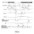
- no_reset 0 (step S101 of FIG. 8) and simultaneously, the counter is reset and counting of the main clock is started ( reference numeral 51 in FIG. 4).
- no_reset 1 (reference numeral 52 in FIG. 4, step S110 of FIG. 8).
- reset_A1 0.
- the main microcomputer reset signal generated by calculating a logical sum of reset_A1 and reset_A2 to the main microcomputer and the main microcomputer is initialized (reference numeral 55 in FIG. 4, step S105 of FIG. 8).
- step S107 of FIG. 8 counting or a signal "wait” constituted by calculating a logical sum of reset_A1 and the sub clock is started by the sub clock switch signal generating counter (reference numeral 56 in FIG. 4, step S107 of FIG. 8), the sub clock switching signal is issued and the sub clock is operated (step S107 of FIG. 8). That is, the sub clock switching control portion 202 starts counting the sub clock at the time of generating the main clock stop flag, issues the sub clock switching signal when the counter is overflowed or reaches the set value and is switched to sub clock operation. When the main clock is recovered and the main clock stop flag is reset by the main clock monitoring portion, the counter is reset and the operation returns to a standby state.
- the sub clock self monitoring portion 203 is provided with the delay adding circuit 405 issuing a signal B constituted by delaying the sub clock by 3/8 period and the delay adding circuit 406 issuing a signal C produced by delaying the signal B by 3/8 period, functions when the main clock stop flag is generated and issues a flag indicating that all the clocks are stopped when the sub clock is stopped.
- the main clock is stopped, the main clock is automatically initialized and when the main clock is recovered thereby, the continuing operation is carried out under a state before abnormality. Further, it is possible that when the main clock cannot be recovered, the continuing operation is carried out by switching the main clock to the sub clock and when the sub clock is also stopped, the flag is issued. That is, the sub clock is provided with a function of monitoring the sub clock per se.
- Reference “A” in FIG. 3 designates the sub clock
- notation “B” designates the clock produced by delaying the sub clock by 3/8 period
- notation “C” designates the clock produced by delaying "B” by 3/8 period.
- reset_A2 in FIG. 3 is "H” and therefore, AND of reset_A2 and an inverted signal of a signal produced by calculating exclusive-OR of A, B, and C, constitutes all clock stop flag.
- the all clock stop flag is issued (step S109 of FIG. 8). The flag can be issued even when the sub clock is stopped in the state of "H” or the state of "L". Further, the delay of 3/8 period is added in generating "B” and "C” because it is determined that the phase relationship is mostly pertinent for preventing occurrence of spike and even when the value of delay is changed, the change naturally falls in the range of the invention.
- FIG. 10 An explanation will be given of a third embodiment of a clock monitoring apparatus according to the invention as follows.
- a main clock temporarily stopping signal for controlling to issue the main microcomputer reset signal, the sub clock switching signal and the all clock stop flag of the above-described first embodiment.
- the sub clock switching control portion of the above-described first embodiment is provided with a sub microcomputer reset signal generating function.
- the sub microcomputer per se can be initialized by a sub microcomputer reset signal generated via a delay circuit.
- the invention realizes that when the main clock is stopped, the main clock is initialized and when the main clock is recovered thereby, the continuing operation is carried out under the state before abnormality. Further, when the main clock is not recovered, the continuing operation can be carried out by switching the main clock to the sub clock. Further, when the sub clock is also stopped, the all clock stop flag can be issued, further, a series of operation can be carried out without control of a software or the like.
- the normal counting signal for monitoring the operational sate of the main clock has been the sub clock in the example of the related art
- the signal is constituted by the high-speed main clock, and therefore a time period until the counter is overflowed or reaches the set value is shortened, and in comparison with the example of the related art there is also achieved an effect of being able to significantly shorten a time period until dealing with the stop of the main clock.
- various modifications can be carried out such as replacing the main microcomputer to a main clock generating apparatus, replacing the sub microcomputer to a system including the circuit of the invention, further, using the main microcomputer initializing signal, the sub clock switching signal and the all clock stop flag by themselves, or using these by various combinations.
Landscapes
- Engineering & Computer Science (AREA)
- Theoretical Computer Science (AREA)
- Physics & Mathematics (AREA)
- General Engineering & Computer Science (AREA)
- General Physics & Mathematics (AREA)
- Nonlinear Science (AREA)
- Microcomputers (AREA)
- Debugging And Monitoring (AREA)
- Manipulation Of Pulses (AREA)
- Synchronisation In Digital Transmission Systems (AREA)
Abstract
A clock monitoring apparatus according to the invention
including a main clock monitoring portion including a first
counter for counting a main clock, issuing a normal operation
confirming flag indicating that a normal operation is being
carried out when the first counter is overflowed or reaches
a previously determined set value, monitoring the normal
operation confirming flag by a sub clock, issuing a first main
clock stop flag having an output in correspondence with H (high
level) / L (low level) of the normal operation confirming flag
and a main clock initializing signal for initializing the main
clock when the main clock is determined to stop and resetting
the first main clock stop flag when the main clock is recovered
by receiving the main clock initializing signal, and a sub
clock switching control portion including a second counter
for counting a signal output produced by calculating a logical
sum of the sub clock and the first main clock stop flag when
the sub clock fails at the time of generating the first
main clock stop flag, switching to a sub clock operation by
issuing a sub clock switching signal when the second counter
output is overflowed or reaches a previously determined set
value and resetting the second counter output when the main
clock is recovered and a second main clock stop flag produced
by inverting the first main clock stop flag and delaying the
sub clock by a predetermined period by a main clock monitoring
portion is reset.
Description
- The present invention relates to a clock monitoring apparatus, particularly to a clock monitoring apparatus controlling a main clock and a sub clock to substitute for each other in failure to thereby realize a stable operation of a microcomputer even when the main clock is stopped.
- Although a monitoring circuit of a clock is used for realizing a stable operation of a microcomputer, when a main clock is stopped, CPU is also stopped and therefore, it is requested for the monitoring circuit to monitor the clock by a signal stably operating even when the main clock is stopped and, when the main clock is stopped, to swiftly deal therewith.
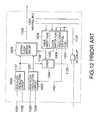
- In order to meet the request, it has been proposed that when the main clock is stopped, the stop of the clock is dealt with by switching the main clock to a sub clock as disclosed in, for example, a prior application (Single chip microcomputer: Japanese Patent Laid-Open No. 7-6155) and a method disclosed in the prior art literature is shown in FIG. 12.
- In a circuit shown in FIG. 12, it is assumed that a
main clock 1102 selected by a systemclock switching circuit 1009 is oscillated normally. Atimer 1004 is for counting asub clock 1101 and during a time period in which themain clock 1102 is normally oscillated, thesub clock 1101 is periodically reset before overflowing by atimer reset signal 1105 outputted from aninternal bus 1201 by receiving execution of instruction in CPU. Therefore, thetimer 1004 is not overflowed and therefore, atimer carry signal 1106 is not issued. - When the
main clock 1102 is stopped, since thetimer reset signal 1105 is not issued, the timer is overflowed, thetimer carry signal 1106 is issued and aclock switch flag 1006 is changed. Thereby, aclock switch signal 1108 is issued and themain clock 1102 is switched to thesub clock 1101. - As described above, according to the prior art, when the main clock is stopped for some cause, the stop is dealt with by switching the main clock to the sub clock and there is not provided a constitution of spontaneously issuing a reset signal and initializing the clock as in the present invention. Therefore, when the main clock is stopped, the main clock is switched to the sub clock which continues operating in a state as it is and there is a drawback that in order to recover an original state, a control or the like by a software is separately needed. Further, since the normally-counted signal is the sub clock, much time is needed until the counter overflows, as a result, there also poses a problem of producing time lag until the stop is dealt with (switch to sub clock) . When the sub clock is stopped, the abnormal stop cannot be detected.
- It is an object of the present invention to provide a clock monitoring apparatus capable of automatically initializing a main clock when the main clock is stopped and continuing operation in a state before abnormality when the main clock is recovered, continuing operation by switching the main clock to a sub clock when the main clock cannot be recovered and issuing a flag when the sub clock is also stopped to thereby achieve stable operation of a microcomputer even when the main clock is stopped.
- According to an aspect of the invention, there is provided a clock monitoring apparatus comprising a main clock monitoring portion including a first counter for counting a main clock, issuing a normal operation confirming flag indicating that a normal operation is being carried out when the first counter is overflowed or reaches a previously determined set value, monitoring the normal operation confirming flag by a sub clock, issuing a first main clock stop flag having an output in correspondence with H (high level) /L (low level) of the normal operation confirming flag and a main clock initializing signal for initializing the main clock when the main clock is determined to stop and resetting the first main clock stop flag when the main clock is recovered by receiving the main clock initializing signal, and a sub clock switching control portion including a second counter for counting a signal output produced by calculating a logical sum of the sub clock and the first main clock stop flag when the sub clock fails at the time of generating the first main clock stop flag, switching to a sub clock operation by issuing a sub clock switching signal when a second counter output is overflowed or reaches a previously determined set value and resetting the second counter output when the main clock is recovered and a second main clock stop flag produced by inverting the first main clock stop flag and delaying the sub clock by a predetermined period by a main clock monitoring portion, is reset.
- The above-mentioned and other objects, features and advantages of this invention will become more apparent by reference to the following detailed description of the invention taken in conjunction with the accompanying drawings, wherein:
- FIG. 1 is a block diagram showing a first embodiment of a clock monitoring apparatus according to the invention;
- FIG. 2 is a diagram showing a clock monitoring system constituted by a main microcomputer and a sub microcomputer including a clock monitoring apparatus according to the invention;
- FIG. 3 is a block diagram showing a detailed constitution of the clock monitoring apparatus of FIG. 1;
- FIG. 4 is a timing chart showing a waveform of operation in the case in which a main clock is stopped when a main clock normal operation confirming flag is 0 and thereafter recovered;
- FIG. 5 is a timing chart showing a waveform of operation in the case in which the main clock is stopped when the main clock normal operation confirming flag is 1 and thereafter recovered;
- FIG. 6 is a timing chart showing a waveform of operation in the case in which the main clock is stopped and switched to a sub clock;
- FIG. 7 is a timing chart showing a waveform of operation when an all clock stop flag is produced;
- FIG. 8 is a flowchart for explaining operation of the clock monitoring apparatus according to the invention;
- FIG. 9 is block diagram showing a second embodiment of a clock monitoring apparatus according to the invention;
- FIG. 10 is a block diagram showing a third embodiment of a clock monitoring apparatus according to the invention;
- FIG. 11 is a block diagram showing a fourth embodiment of a clock monitoring apparatus according to the invention; and
- FIG. 12 is a block diagram showing an example of a clock monitoring apparatus of the prior art.
-
- An explanation will be given of a first embodiment of a clock monitoring apparatus according to the invention in reference to the drawings. The clock monitoring apparatus according to the invention is integrated into a clockmonitoring system shown in FIG. 2. The system comprises a
main microcomputer 301 and asub microcomputer 302 and the clock monitoring apparatus is included to a side of thesub microcomputer 302. FIG. 1 is a block diagram showing a constitution of the clock monitoring apparatus and FIG. 3 is a block diagram showing a further detailed constitution of the clock monitoring apparatus. - In FIG. 1, a
clock monitoring apparatus 200 includes a mainclock monitoring portion 201 including a counter, a sub clockswitching control portion 202 including a counter, and a sub clockself monitoring portion 203 including a delay adding circuit and an exclusive-OR circuit. - In detail , as shown by FIG. 3, the
clock monitoring apparatus 200 is constituted by a mainclock monitoring circuit 401, a reset_A1flag generating circuit 402, a reset_A2flag generating circuit 403, a sub clock switchsignal generating counter 404 and delay addingcircuits clock monitoring portion 201 is constituted by the mainclock monitoring circuit 401, the reset_A1 flag generatingcircuit 402, the reset_A2flag generating circuit 403 and a logical sum circuit (OR gate) and the sub clockswitching control portion 202 is constituted by a logical sum circuit (OR gate) and the sub clock switchsignal generating counter 404. - The main
clock monitoring circuit 401 counts a main clock by the included counter and issues a normal operation confirming flag no_reset constituting "H" ("1", that is, signifying high level) indicating that normal operation is being carried out when then counter is equal to a predetermined set value, or overflowed. The flag no_reset is monitored at fall of a sub clock. The reset_A1 flag generatingcircuit 402 issues a flag reset_A1 constituting "H" when the no_reset is "H" and "L" when the no_reset is "L" ("0", that is, signifying low level) . The reset_A2 flag generatingcircuit 403 issues a main clock stop flag reset_A2 inverting the flag reser_A1 and delaying by a half period of the sub clock and issues a main clock initializing (main microcomputer resetting) signal. However, the reset_A2 flag generatingcircuit 403 issues the signals only when the main clock is determined to stop. When the main clock is recovered by receiving the main clock initializing signal, the reset_A2flag generating circuit 403 continues operating as it is by resetting the main clock stop flag reset_A2. - Next, an explanation will be given of operation of the clock monitoring apparatus having the above-described constitution in reference to FIG. 4 through FIG. 8. First, an explanation will be given of a case of normal operation.
- The main clock is counted and there is generated the signal no_reset constituting "H" when the counter is equal to the set value or overflowed by the counter. At rise of the sub clock, no_reset=0 (step S101 of FIG. 8) and simultaneously, the counter is reset and counting of the main clock is started (
reference numeral 51 in FIG. 4). - When the main clock is equal to the set value of the counter or overflowed (Yes at step S102 of FIG. 8), no_reset=1 (
reference numeral 52 in FIG. 4, step S110 of FIG. 8). - At fall of the sub clock, no_reset=1 (step S111 of FIG. 8) and therefore, the reset_A1 stays to be "H" and the main microcomputer reset signal is not issued (
reference numeral 53 in FIG. 4). - Next, an explanation will be given of a case in which the main clock is stopped, the main microcomputer is initialized, and as a result, the main clock is recovered. When the main clock is stopped, the counter is not overflowed or does not reach the predetermined set value (No at step S102 of FIG. 8). Therefore, the flag no_reset stays to be "L" and the reset_A1 stays to be "H" (step S103 of FIG. 8). Further, even when a time period of stopping the main clock is a time period of "H" of no_reset or a time period of "L" thereof, the main clock is operated without problem. As shown by FIG. 7, when the main clock is stopped during a time period from rise of no_reset to fall of the sub clock thereafter, the main microcomputer reset signal is generated at fall of the sub clock one period thereafter (
reference numeral 54 in FIG. 4). - In the case in which no_reset=0 at fall of the sub clock, reset_A1=0. There is generated the flag reset_A2 constituted by inverting the reset_A1 and delaying by a half period of the sub clock. Therefore, in this case, at rise of the sub clock, reset_A2=1 (step S104 of FIG. 8). There is issued the main microcomputer reset signal generated by calculating a logical sum of reset_A1 and reset_A2 to the main microcomputer and the main microcomputer is initialized (
reference numeral 55 in FIG. 4, step S105 of FIG. 8). - At this occasion, counting or a signal "wait" constituted by calculating a logical sum of reset_A1 and the sub clock is started by the sub clock switch signal generating counter (
reference numeral 56 in FIG. 4, step S107 of FIG. 8), the sub clock switching signal is issued and the sub clock is operated (step S107 of FIG. 8). That is, the sub clockswitching control portion 202 starts counting the sub clock at the time of generating the main clock stop flag, issues the sub clock switching signal when the counter is overflowed or reaches the set value and is switched to sub clock operation. When the main clock is recovered and the main clock stop flag is reset by the main clock monitoring portion, the counter is reset and the operation returns to a standby state. - When the main clock is recovered before the sub clock switch signal generating counter is overflowed, the counter in the main
clock monitoring circuit 401 is overflowed again and no_reset=1 (reference numeral 57 in FIG. 4, step S110 of FIG. 8). - In the case of no_reset=1 at fall of the sub clock, reset_A1=1, reset_A2 becomes "L" at rise of the sub clock. The sub clock switch signal generating counter is reset at fall of reset_A2 and therefore, the operation is not switched to the sub clock (
reference numeral 58 in FIG. 4). - Next, an explanation will be given of a case in which even when the main clock is stopped and the main microcomputer is initialized, the main clock stays to be stopped in reference to FIG. 6. After initializing the main microcomputer by the above-described procedure, there is counted an output of a signal "wait" constituted by calculating the logical sum of reset_A1 and the sub clock by the sub clock switch signal generating counter (
reference numeral 61 in FIG. 4). - When the main clock is not recovered (
notation 62 in FIG. 4), the sub clock switch signal generating counter is overflowed and the sub clock switching signal is issued (reference numeral 63 in FIG. 4). - Further, an explanation will be given of a case in which after switching the operation clock to the sub clock, the sub clock is stopped in reference to FIG. 3 and FIG. 7. The sub clock
self monitoring portion 203 is provided with thedelay adding circuit 405 issuing a signal B constituted by delaying the sub clock by 3/8 period and thedelay adding circuit 406 issuing a signal C produced by delaying the signal B by 3/8 period, functions when the main clock stop flag is generated and issues a flag indicating that all the clocks are stopped when the sub clock is stopped. By the function, it is possible that when the main clock is stopped, the main clock is automatically initialized and when the main clock is recovered thereby, the continuing operation is carried out under a state before abnormality. Further, it is possible that when the main clock cannot be recovered, the continuing operation is carried out by switching the main clock to the sub clock and when the sub clock is also stopped, the flag is issued. That is, the sub clock is provided with a function of monitoring the sub clock per se. - A specific explanation will be given of operation of the sub clock
self monitoring portion 203 as follows . Reference "A" in FIG. 3 designates the sub clock, notation "B" designates the clock produced by delaying the sub clock by 3/8 period and notation "C" designates the clock produced by delaying "B" by 3/8 period. - When the main clock is stopped (step S108 of FIG. 8), reset_A2 in FIG. 3 is "H" and therefore, AND of reset_A2 and an inverted signal of a signal produced by calculating exclusive-OR of A, B, and C, constitutes all clock stop flag. When the sub clock is stopped, after 3/4 period, the all clock stop flag is issued (step S109 of FIG. 8). The flag can be issued even when the sub clock is stopped in the state of "H" or the state of "L". Further, the delay of 3/8 period is added in generating "B" and "C" because it is determined that the phase relationship is mostly pertinent for preventing occurrence of spike and even when the value of delay is changed, the change naturally falls in the range of the invention.
- An explanation will be given of a second embodiment of a clock monitoring apparatus according to the invention as follows. According to the embodiment, as shown in FIG. 9, the sub clock self monitoring portion is deleted in the above-described first embodiment. Although the all clock stop flag cannot be issued thereby, since the delay adding circuits and the exclusive-OR circuit are dispensed with, the circuit scale can be reduced.
- An explanation will be given of a third embodiment of a clock monitoring apparatus according to the invention as follows. According to the embodiment, as shown in FIG. 10, there is added a main clock temporarily stopping signal for controlling to issue the main microcomputer reset signal, the sub clock switching signal and the all clock stop flag of the above-described first embodiment. Thereby, even when the user intentionally stops the main clock by a signal of temporarily stopping the main clock such as HALT, the respective output signals are not issued.
- An explanation will be given of a fourth embodiment of a clock monitoring apparatus according to the invention as follows. According to the embodiment, as shownin FIG. 11, the sub clock switching control portion of the above-described first embodiment is provided with a sub microcomputer reset signal generating function. Thereby, after switching to a sub clock operation mode, the sub microcomputer per se can be initialized by a sub microcomputer reset signal generated via a delay circuit.
- In this way, the invention realizes that when the main clock is stopped, the main clock is initialized and when the main clock is recovered thereby, the continuing operation is carried out under the state before abnormality. Further, when the main clock is not recovered, the continuing operation can be carried out by switching the main clock to the sub clock. Further, when the sub clock is also stopped, the all clock stop flag can be issued, further, a series of operation can be carried out without control of a software or the like.
- Further, although the normal counting signal for monitoring the operational sate of the main clock has been the sub clock in the example of the related art, according to the invention the signal is constituted by the high-speed main clock, and therefore a time period until the counter is overflowed or reaches the set value is shortened, and in comparison with the example of the related art there is also achieved an effect of being able to significantly shorten a time period until dealing with the stop of the main clock.
- Further, in the above-described embodiments, various modifications can be carried out such as replacing the main microcomputer to a main clock generating apparatus, replacing the sub microcomputer to a system including the circuit of the invention, further, using the main microcomputer initializing signal, the sub clock switching signal and the all clock stop flag by themselves, or using these by various combinations.
- Although the invention has been described with reference to specific embodiments, this description is not meant to be construed in a limiting sense. Various modifications of the disclosed embodiments will become apparent to persons skilled in the art upon reference to the description of the invention. It is therefore contemplated that the appended claims will cover any modifications or embodiments as fall within the true scope of the invention.
Claims (10)
- A clock monitoring apparatus comprising:a main clock monitoring portion including a first counter for counting a main clock, issuing a normal operation confirming flag indicating that a normal operation is being carried out when the first counter is overflowed or reaches a previously determined set value, monitoring the normal operation confirming flag by a sub clock, issuing a first main clock stop flag having an output in correspondence with H (high level) / L (low level) of the normal operation confirming flag and a main clock initializing signal for initializing the main clock when the main clock is determined to stop and resetting the first main clock stop flag when the main clock is recovered by receiving the main clock initializing signal; anda sub clock switching control portion including a second counter for counting a signal output produced by calculating a logical sum of the sub clock and the first main clock stop when the sub clock fails at the time of generating the first main clock stop flag, switching to a sub clock operation by issuing a sub clock switching signal when the second counter output is overflowed or reaches a previously determined set value and resetting the second counter output when the main clock is recovered and a second main clock stop flag produced by inverting the first main clock stop flag and delaying the sub clock by a predetermined period by a main clock monitoring portion is reset.
- The clock monitoring apparatus according to claim 1, wherein the second main clock stop flag generating portion outputs the main clock initializing signal by calculating a logical sum of the first main clock stop flag and the second main clock stop flag.
- The clock monitoring apparatus according to claim 2, further comprising:a first logical product circuit for calculating a logical product of a main clock temporarily stopping signal for temporarily stopping the main clock and an output signal from the first logical sum circuit; anda second logical product circuit for calculating a logical product of the main clock temporarily stop signal and an output signal from the second counter.
- The clock monitoring apparatus according to claim 1, wherein the main clock monitoring portion comprising:a main clock monitoring circuit for counting the main clock by the first counter, issuing the normal operation confirming flag when the first counter is equal to the predetermined set value or overflowed and monitoring the normal operation confirming flag at fall of the sub clock;a first main clock stop flag generating portion for issuing the first main clock stop flag constituting "H" when the normal operation confirming flag is "H" and constituting "L" when the normal operation confirming flag is "L" at fall of the sub clock; anda second main clock stop flag generating portion for issuing the second main clock stop flag and the main clock initializing signal when the main clock is stopped.
- The clock monitoring apparatus according to claim 1, wherein when the main clock is recovered by receiving the main clock initializing signal, the main clock monitoring portion resets the second main clock stop flag.
- The clock monitoring apparatus according to claim 1, wherein the sub clock switching control portion includes a second logical sum circuit for calculating a logical sum of the first main clock stop flag and the sub clock, making the second counter count the logical sum signal at a time point of generating the main clock stop flag, switching to the sub clock operation by issuing the sub clock switching signal when the second counter is overflowed or reaches the set value and returning to a standby state by resetting the second counter when the main clock is recovered and the main clock stop flag is reset.
- The clock monitoring apparatus according to claim 6, wherein in a case in which the main clock remains stopped even when the main clock is stopped and the main microcomputer is initialized, the second counter is overflowed and a sub clock switching signal is issued by the sub clock switching control portion.
- The clock monitoring apparatus according to claim 1, further comprising:a sub clock self monitoring portion capable of issuing an all clock stop flag indicating that all the clocks are stopped when the sub clock is stopped, initializing automatically the main clock when the main clock is stopped and carrying out a continuing operation under a state before abnormality when the main clock is recovered thereby.
- The clock monitoring apparatus according to claim 8:
wherein the sub clock selfmonitorlngportion comprising:wherein an all clock stop flag is outputted from the third logical product circuit.a first delaying adding circuit for issuing a first delay signal for delaying the sub clock by a predetermined period and a second delay adding circuit for issuing a second delay signal for delaying the first delay signal by the predetermined period;an exclusive-OR circuit for calculating an exclusive-OR of the sub clock, the first delay signal and the second delay signal; anda third logical product circuit for calculating a logical product of the second main clock stop flag and an inverted signal of a signal produced by calculating the exclusive-OR; - The clock monitoring apparatus according to claim 9, further comprising:a first logical product circuit for calculating a logical product of a main clock temporarily stopping signal for temporarily stopping the main clock and an output signal from the first logical sum circuit;a second logical product circuit for calculating a logical product of the main clock temporarily stopping signal and an output signal from the second counter; anda third logical product circuit for calculating a logical product of the main clock temporarily stopping signal and an output signal from the third logical sum circuit.
Applications Claiming Priority (2)
| Application Number | Priority Date | Filing Date | Title |
|---|---|---|---|
| JP2001283579 | 2001-09-18 | ||
| JP2001283579A JP3523225B2 (en) | 2001-09-18 | 2001-09-18 | Clock monitoring apparatus and monitoring method |
Publications (1)
| Publication Number | Publication Date |
|---|---|
| EP1293875A2 true EP1293875A2 (en) | 2003-03-19 |
Family
ID=19107044
Family Applications (1)
| Application Number | Title | Priority Date | Filing Date |
|---|---|---|---|
| EP02090338A Withdrawn EP1293875A2 (en) | 2001-09-18 | 2002-09-18 | Clock monitoring apparatus |
Country Status (4)
| Country | Link |
|---|---|
| US (2) | US6670839B2 (en) |
| EP (1) | EP1293875A2 (en) |
| JP (1) | JP3523225B2 (en) |
| KR (1) | KR20030024619A (en) |
Cited By (2)
| Publication number | Priority date | Publication date | Assignee | Title |
|---|---|---|---|---|
| DE102007022369A1 (en) * | 2007-05-07 | 2008-11-20 | IHP GmbH - Innovations for High Performance Microelectronics/Institut für innovative Mikroelektronik | Clock monitoring circuit for e.g. application-specific integrated circuit, has testing circuit for testing whether next level change of detailed clock signal takes place, before and after testing clock signal |
| EP2090949A3 (en) * | 2008-02-18 | 2010-12-01 | Shibuya Kogyo Co., Ltd. | Article processing system |
Families Citing this family (13)
| Publication number | Priority date | Publication date | Assignee | Title |
|---|---|---|---|---|
| DE60233485D1 (en) * | 2001-05-25 | 2009-10-08 | Imaging Therapeutics Inc | METHOD FOR DIAGNOSIS, TREATMENT AND PREVENTION OF BONE LOSS |
| JP3523225B2 (en) * | 2001-09-18 | 2004-04-26 | Necマイクロシステム株式会社 | Clock monitoring apparatus and monitoring method |
| US20030115503A1 (en) * | 2001-12-14 | 2003-06-19 | Koninklijke Philips Electronics N.V. | System for enhancing fault tolerance and security of a computing system |
| JP3593104B2 (en) * | 2002-01-11 | 2004-11-24 | 沖電気工業株式会社 | Clock switching circuit |
| JP4082211B2 (en) * | 2002-12-27 | 2008-04-30 | 株式会社デンソー | Microcomputer |
| US20080140890A1 (en) * | 2004-02-27 | 2008-06-12 | Koninklijke Philips Electronics N.V. | Electronic Circuit Arrangement For Detecting a Failing Clock |
| JP4698518B2 (en) * | 2006-07-27 | 2011-06-08 | 富士通セミコンダクター株式会社 | Verification support device, verification support method, and program |
| GB2456937B (en) * | 2006-10-24 | 2011-07-13 | Bradley Fixtures Corp | Capacitive sensing for washroom fixture |
| JP2010268105A (en) * | 2009-05-13 | 2010-11-25 | Renesas Electronics Corp | Microcomputer |
| JP6701869B2 (en) * | 2016-03-25 | 2020-05-27 | セイコーエプソン株式会社 | Circuit device, physical quantity detection device, electronic device and moving body |
| US10459501B2 (en) * | 2017-07-28 | 2019-10-29 | Western Digital Technologies, Inc. | System and method for augmentation of reset recovery operation timing |
| KR102408439B1 (en) * | 2017-12-26 | 2022-06-14 | 에스케이하이닉스 주식회사 | Clock monitoring circuit |
| TWI779930B (en) * | 2021-11-18 | 2022-10-01 | 新唐科技股份有限公司 | Clock monitor circuit, microcontroller, and control method thereof |
Family Cites Families (6)
| Publication number | Priority date | Publication date | Assignee | Title |
|---|---|---|---|---|
| US4653054A (en) * | 1985-04-12 | 1987-03-24 | Itt Corporation | Redundant clock combiner |
| JPH076155A (en) | 1993-06-15 | 1995-01-10 | Nec Ic Microcomput Syst Ltd | Single chip microcomputer |
| US5642069A (en) * | 1994-04-26 | 1997-06-24 | Unisys Corporation | Clock signal loss detection and recovery apparatus in multiple clock signal system |
| JPH10124167A (en) * | 1996-10-17 | 1998-05-15 | Miyagi Oki Denki Kk | System clock switching device |
| JP2000122749A (en) * | 1998-10-20 | 2000-04-28 | Mitsubishi Electric Corp | Oscillation stop detector |
| JP3523225B2 (en) * | 2001-09-18 | 2004-04-26 | Necマイクロシステム株式会社 | Clock monitoring apparatus and monitoring method |
-
2001
- 2001-09-18 JP JP2001283579A patent/JP3523225B2/en not_active Expired - Fee Related
-
2002
- 2002-09-13 US US10/242,415 patent/US6670839B2/en not_active Expired - Lifetime
- 2002-09-17 KR KR1020020056396A patent/KR20030024619A/en active IP Right Grant
- 2002-09-18 EP EP02090338A patent/EP1293875A2/en not_active Withdrawn
-
2003
- 2003-11-04 US US10/699,777 patent/US6943590B2/en not_active Expired - Lifetime
Cited By (2)
| Publication number | Priority date | Publication date | Assignee | Title |
|---|---|---|---|---|
| DE102007022369A1 (en) * | 2007-05-07 | 2008-11-20 | IHP GmbH - Innovations for High Performance Microelectronics/Institut für innovative Mikroelektronik | Clock monitoring circuit for e.g. application-specific integrated circuit, has testing circuit for testing whether next level change of detailed clock signal takes place, before and after testing clock signal |
| EP2090949A3 (en) * | 2008-02-18 | 2010-12-01 | Shibuya Kogyo Co., Ltd. | Article processing system |
Also Published As
| Publication number | Publication date |
|---|---|
| US20040090245A1 (en) | 2004-05-13 |
| US20030052722A1 (en) | 2003-03-20 |
| US6943590B2 (en) | 2005-09-13 |
| KR20030024619A (en) | 2003-03-26 |
| US6670839B2 (en) | 2003-12-30 |
| JP2003091329A (en) | 2003-03-28 |
| JP3523225B2 (en) | 2004-04-26 |
Similar Documents
| Publication | Publication Date | Title |
|---|---|---|
| EP1293875A2 (en) | Clock monitoring apparatus | |
| CN114499732B (en) | Clock calibration method, clock calibration device, computer equipment and readable storage medium | |
| US8892923B2 (en) | Data processing apparatus and method for maintaining a time count value in normal and power saving modes of operation | |
| JP3072720B2 (en) | Information processing device | |
| US7284142B2 (en) | Real time interrupt module for operating systems and time triggered applications | |
| US20050212571A1 (en) | Automatic selection of an on-chip ancillary internal clock generator upon resetting a digital system | |
| JPH1153201A (en) | Method and device for processing plural interruptions | |
| CN110795289B (en) | Multi-clock automatic switching method | |
| JPH07334392A (en) | Resetting device and abnormal operation detector | |
| EP0837448A2 (en) | Microcomputer with controller operating in syschronism with external synchronoussignal | |
| CN113485185B (en) | Method for N times redundancy control system | |
| US11169892B1 (en) | Detecting and reporting random reset faults for functional safety and other high reliability applications | |
| JP3137025B2 (en) | Runaway detection method for data processing system | |
| JPH11316615A (en) | Power noise preventing circuit for mcu | |
| KR100269348B1 (en) | Radio lan system having auto-restarting circuit | |
| JP2749994B2 (en) | Numerical control unit | |
| JPH103324A (en) | Information processor having high reliability clock | |
| JP2003099161A (en) | System for starting information processing system | |
| KR100208295B1 (en) | Clock monitor | |
| CN117729129A (en) | Latent error detection method, device, communication unit and network equipment | |
| JPH0973404A (en) | Watchdog timer circuit | |
| JPH0756862A (en) | System for synchronizing multiprocessor system | |
| JP2001325870A (en) | Input circuit for control signal | |
| JP2011134063A (en) | Watchdog timer | |
| JPH0573360A (en) | Watchdog timer |
Legal Events
| Date | Code | Title | Description |
|---|---|---|---|
| PUAI | Public reference made under article 153(3) epc to a published international application that has entered the european phase |
Free format text: ORIGINAL CODE: 0009012 |
|
| AK | Designated contracting states |
Kind code of ref document: A2 Designated state(s): AT BE BG CH CY CZ DE DK EE ES FI FR GB GR IE IT LI LU MC NL PT SE SK TR Designated state(s): AT BE BG CH CY CZ DE DK EE ES FI FR GB GR IE IT LI LU MC NL PT SE SK TR |
|
| AX | Request for extension of the european patent |
Extension state: AL LT LV MK RO SI |
|
| RAP1 | Party data changed (applicant data changed or rights of an application transferred) |
Owner name: NEC ELECTRONICS CORPORATION |
|
| STAA | Information on the status of an ep patent application or granted ep patent |
Free format text: STATUS: THE APPLICATION HAS BEEN WITHDRAWN |
|
| 18W | Application withdrawn |
Effective date: 20040706 |