EP1291817A1 - Détection d'une variation de l'environnement d'un circuit intégré - Google Patents
Détection d'une variation de l'environnement d'un circuit intégré Download PDFInfo
- Publication number
- EP1291817A1 EP1291817A1 EP02354131A EP02354131A EP1291817A1 EP 1291817 A1 EP1291817 A1 EP 1291817A1 EP 02354131 A EP02354131 A EP 02354131A EP 02354131 A EP02354131 A EP 02354131A EP 1291817 A1 EP1291817 A1 EP 1291817A1
- Authority
- EP
- European Patent Office
- Prior art keywords
- delay
- circuit
- integrated circuit
- word
- current
- Prior art date
- Legal status (The legal status is an assumption and is not a legal conclusion. Google has not performed a legal analysis and makes no representation as to the accuracy of the status listed.)
- Granted
Links
Images


Classifications
-
- G—PHYSICS
- G06—COMPUTING OR CALCULATING; COUNTING
- G06K—GRAPHICAL DATA READING; PRESENTATION OF DATA; RECORD CARRIERS; HANDLING RECORD CARRIERS
- G06K19/00—Record carriers for use with machines and with at least a part designed to carry digital markings
- G06K19/06—Record carriers for use with machines and with at least a part designed to carry digital markings characterised by the kind of the digital marking, e.g. shape, nature, code
- G06K19/067—Record carriers with conductive marks, printed circuits or semiconductor circuit elements, e.g. credit or identity cards also with resonating or responding marks without active components
- G06K19/07—Record carriers with conductive marks, printed circuits or semiconductor circuit elements, e.g. credit or identity cards also with resonating or responding marks without active components with integrated circuit chips
- G06K19/0716—Record carriers with conductive marks, printed circuits or semiconductor circuit elements, e.g. credit or identity cards also with resonating or responding marks without active components with integrated circuit chips at least one of the integrated circuit chips comprising a sensor or an interface to a sensor
-
- G—PHYSICS
- G06—COMPUTING OR CALCULATING; COUNTING
- G06K—GRAPHICAL DATA READING; PRESENTATION OF DATA; RECORD CARRIERS; HANDLING RECORD CARRIERS
- G06K19/00—Record carriers for use with machines and with at least a part designed to carry digital markings
- G06K19/06—Record carriers for use with machines and with at least a part designed to carry digital markings characterised by the kind of the digital marking, e.g. shape, nature, code
- G06K19/067—Record carriers with conductive marks, printed circuits or semiconductor circuit elements, e.g. credit or identity cards also with resonating or responding marks without active components
- G06K19/07—Record carriers with conductive marks, printed circuits or semiconductor circuit elements, e.g. credit or identity cards also with resonating or responding marks without active components with integrated circuit chips
- G06K19/073—Special arrangements for circuits, e.g. for protecting identification code in memory
-
- G—PHYSICS
- G06—COMPUTING OR CALCULATING; COUNTING
- G06K—GRAPHICAL DATA READING; PRESENTATION OF DATA; RECORD CARRIERS; HANDLING RECORD CARRIERS
- G06K19/00—Record carriers for use with machines and with at least a part designed to carry digital markings
- G06K19/06—Record carriers for use with machines and with at least a part designed to carry digital markings characterised by the kind of the digital marking, e.g. shape, nature, code
- G06K19/067—Record carriers with conductive marks, printed circuits or semiconductor circuit elements, e.g. credit or identity cards also with resonating or responding marks without active components
- G06K19/07—Record carriers with conductive marks, printed circuits or semiconductor circuit elements, e.g. credit or identity cards also with resonating or responding marks without active components with integrated circuit chips
- G06K19/073—Special arrangements for circuits, e.g. for protecting identification code in memory
- G06K19/07309—Means for preventing undesired reading or writing from or onto record carriers
- G06K19/07372—Means for preventing undesired reading or writing from or onto record carriers by detecting tampering with the circuit
Definitions
- the present invention relates to the field of circuits and, more specifically, the detection of variations of environmental parameters of an integrated circuit chip in operation.
- Monitoring systems for variables related to the environment of an integrated circuit such as temperature, supply voltage, etc., are used in particular to detect a possible violation of the integrated circuit chip in protected systems. It may be, for example, to detect possible external interventions to the integrated circuit in the purpose of hacking data it contains. This last application relates more particularly to smart cards.
- Another example of application of surveillance systems of an environmental variable of an integrated circuit is the operating authorization of such a circuit in relation to a range, for example of temperatures, for which the circuit is destined.
- the monitoring elements are dedicated to a given variable. For example, we use a voltage of threshold for detecting possible temperature variations, and the results of the measure are interpreted determine a possible violation of the external environment of the chip.
- a disadvantage is that we have to multiply the number of detection circuits with the number of variables or parameters that we want to monitor.
- Another disadvantage is that getting a measurement analog requires a conversion to be interpreted by a digital system generally equipping the circuit chip integrated, in order to decide on the consequences of the eventual violation.
- Another disadvantage is that a variation of the parameters environmental remedies can occur without a violation of the chip.
- the external conditions of temperature can be significantly modified (several dozens of degrees). It would be desirable to be able to distinguish variation related to a violation of a variation related to a normal change of operating conditions.
- the present invention aims to propose a new method detecting variations of at least one environmental parameter an integrated circuit that overcomes the disadvantages of known solutions.
- the object of the invention is more particularly to propose a solution which, by means of the same circuit, allows to monitor several environmental parameters of the integrated circuit.
- the invention also aims to detect a deviation of the parameters compared to a reference value.
- the invention also aims to propose a solution avoiding the use of analog / digital converters measurement results.
- the invention also aims to allow an adaptation automatic detection system to normal variations environment.
- comparing a measured current delay with two values predetermined threshold defining a range of operation authorized circuit comparing a measured current delay with two values predetermined threshold defining a range of operation authorized circuit.
- a current delay is compared with a reference value unique.
- the value of a programmable delay element is enslaved function of the difference between the current value and the value of reference, the range of possible variation preferably being predetermined.
- said delay elements are in parallel and have their common input terminal connected at the output of a delay element programmable with an input terminal constitutes a terminal input of the detection circuit.
- said comparator provides a self-timer configuration word programmable from a comparison of the current value compared to a reference value.
- the circuit comprises means for setting a range of variation programmable delay.
- said delay elements are in series.
- the circuit further comprises an intermediate delay element inserted between an application terminal of a trigger signal the respective clock entries of the different flip-flops.
- a feature of the present invention is to evaluate a propagation delay of an electrical signal in delaying elements which are individually sensitive to variations of the integrated circuit environment.
- the invention takes advantage of the fact that many parameters environmental aspects of an integrated circuit, that is to say parameters that are not directly related to the structure internal circuit, such as temperature or supply voltage of the circuit, are likely when vary, change the delay of propagation of a signal in an electric path.
- the invention uses this property for detect variations, more precisely with respect to a reference value, of one or more environmental parameters of the integrated circuit, without the need to measure directly this or these parameters.
- Figure 1 represents, very schematically, a embodiment of an integrated circuit 1 equipped with a circuit 2 detection device according to the present invention. Only circuit 2 has been represented as a block contained in the circuit integrated 1, which for the rest is any circuit.
- Circuit 1 is powered by at least one voltage V provided, for example, by a generator 3.
- the supply voltage V of circuit 1 constitutes, within the meaning of the invention, an environmental parameter of this circuit.
- a Another environmental parameter illustrated in Figure 1 is the temperature T to which circuit 1 is subjected.
- temperature T can come from the internal heating of the circuit related to its operation or an external source. In all the case, this constitutes, within the meaning of the invention, also a environmental parameter.
- Other environmental parameters can influence the propagation time of a signal. he This is, for example, the stability of the voltage power supply, humidity, radiation, etc.
- the detection circuit 2 comprises essentially a measuring circuit 21 of propagation time a triggering edge of a measurement, more precisely a state change of a binary signal.
- the exit of the circuit 21 is connected to the input of a comparator 22 of which another input receives a reference REF of comparison.
- the exit of comparator 22 provides the result of a possible delay deviation compared to the reference delay.
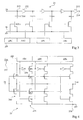
- FIG. 2 represents a first embodiment of a detection circuit 2 according to the present invention.
- the circuit 21 for measuring propagation times essentially comprises n retarding elements 211 (C1, ..., Ci, ..., Cn) or electrical paths introducing preferentially different delays from each other.
- the exits respective elements 211 are connected to the inputs of data (D) of n flip-flops 212 (D1, ..., Di, ..., Dn).
- the respective outputs (eg the direct outputs Q) of the flip-flops 212 directly supply n bits (B1, ..., Bi, ..., Bn) of a binary word representative of the measurement carried out.
- the bits of the word are written in a register 213 or any other similar temporary storage element.
- the different delay elements 211 are placed in parallel to each other. Their respective input terminals are therefore connected together.
- a front to which we wish apply the different delays is applied on a terminal 24 circuit 2.
- This terminal 24 is connected to a circuit input 25 introducing an adjustable delay and serving, as we will see it later, to an automatic adaptation (calibration) of the circuit 2.
- the circuit 25 or "adjustable buffer” (BUF) has its output 251 connected to the respective inputs of retarding elements 211.
- the respective clock inputs Ck of the flip-flops 212 are connected together for the reading of the binary states present at the input of the different flip-flops is simultaneous for the n flip-flops.
- a CLK trigger signal of reading applied to a terminal 23 of circuit 2 passes through a additional delay element 215.
- the element 215 introduces a delay corresponding to the average delay (Cav) of the different electric paths introduced by the elements 211 (taking account of the flip-flops 212 adding an identical delay for all paths).
- the self-timer 215 is optional. He basically to enable the use of a corresponding CLK signal to the binary signal providing the front on terminal 24. In this case, the terminals 23 and 24 are combined. The self-timer 215 then allows to delay the reading of the present data on the inputs of flip-flops 212 of the time required for average propagation in electric paths 211.
- the circuit (not shown) for generating the front of measurement provides the clock signal of the latches with delay. he is, for example, a processor (integrated or not in the circuit 1) to control variations and trigger actions adapted.
- this front arrives on the respective D inputs of the flip-flops 212 at different times according to the importance of the delays due to the respective elements 211 and the delay related to the circuit 25 common to all electrical paths. All electrical paths which generate a delay greater than the corresponding Cav delay at item 215 provide a bit in state "0" in the extent to which the front applied to the input 24 is not theirs still arrived. All paths that generate a lower delay to the Cav delay provide a bit in the state "1" as far as the front arrives on the D input of the corresponding flip-flop before the expiry of the period Cav.
- the possible variation of the delay of the different paths gives an indirect indication of the drift of the external environment of the integrated circuit, whether in terms of temperature or supply voltage.
- any elements integrated components of retarding elements may be, for example, oxide or metal resistors.
- the delay elements other forms, provided that they are sensitive to environmental parameters that one wishes to measure for the circuit.
- the choice of the range of variation of the delays provided by the different elements depends on the application and desired sensitivity.
- the circuit 2 further comprises a comparator 22 (COMP) whose first input receives the binary word B1, ..., Bi, ..., Bn temporarily stored in the register 213 and whose a second reference input receives a binary word of reference (Br1, ..., Bri, ..., Brn) previously stored in a register 221 or the like.
- the result of the comparison is provided on an output terminal 222 of the comparator 22.
- comparator 22 further comprises n outputs 223 to the circuit 25. These n outputs provide a binary word ⁇ B1, ..., ⁇ Bn of n bits used to recalibrate the circuit 25 if necessary as will be detailed later.
- the delays caused by the elements 211 are increasing (or decreasing) with the weight of the bit corresponding in the word delivered by the flip-flops 212.
- the gap between the respective weights of the first bits in state 0 (respectively at state 1) of the measured word and the reference word then provides an indication of the magnitude of the variation in environmental parameters. This indication can be used, for example, to calculate the rate of change of environmental parameters by successive measurements.
- a relatively slow variation related to normal changes in operating conditions eg example, a static variation of the supply voltage
- sudden change for example, dynamic instability of the supply voltage
- the reference binary word stored in the register 221 is obtained in a parameterization phase of circuit 2.
- This phase is performed under reference conditions (by example, under a reference controlled supply voltage and at a temperature of 25 ° C).
- the circuit is then characterized under the conditions of functioning corresponding to extreme conditions upper and lower.
- the characterization phase of the circuit allows to obtain two extreme binary values framing the value of reference BREF. The difference between the two values corresponds to the authorized beach. Extreme values are used to configure (for example, by means of a series of programmable switches) the circuit 25 to define a possible adjustment range for slow down or accelerate the front applied on terminal 24.
- the adjustment loop thus obtained then makes it possible each characterization phase, to replace the circuit extraction of the measured binary word (electrical paths 211, 212) under reference conditions.
- the two extreme values binary words beyond which the adaptation circuit no longer sufficient are the boundary conditions environment that we have set sacred.
- the comparator 22 In operation, as soon as circuit 25 is no longer able to refocus the system on the reference word, the comparator 22 outputs a signal (in practice a change binary status) indicator of a violation of the conditions environment for which the circuit is provided.
- An advantage of the invention is that it provides a global monitoring circuit of a set of variables environmental aspects of the integrated circuit.
- the inventors are seen that, most often, what is important is detect a deviation from the allowed operating range any of the parameters.
- Another advantage of the invention is that the input-output of the detection circuit are, because of the nature same circuit, digital without the need to perform any conversion.
- Another advantage of the invention is that by allowing a digital adaptation or calibration of the element 25, we make this adaptation insensitive to the measured external conditions (especially the temperature).
- Another advantage of the invention is that the circuit can easily be integrated in an integrated circuit chip, in particular of the smart card type.
- FIG. 3 represents a first exemplary embodiment of a circuit 25 for adapting the measuring circuit 2 according to the invention.
- a plurality of gates 252 connected in series between the input terminal 24 of the circuit 25 and its output terminal 251.
- the gates 252 are for example, simple non-inverting elements of the "buffer" type.
- the respective inputs 253 of the doors 252 are connected individually to a first terminal of a capacitor C254 whose other terminal is connected to ground (M) by a switch K255 (for example, a MOS transistor). Grids of different K255 transistors respectively receive one of the bits ⁇ B1, ⁇ B2, ..., ⁇ Bi, ..., ⁇ Bn of the programming word supplied by the comparator 22 ( Figure 2).
- the respective values of capacitors C254 are different depending on the weight of the bit in the binary word ⁇ B.
- the programming word can be obtained different ways. For example, we can use directly the bitwise difference between the measured word 213 ( Figure 2) and the reference word. We can also use more complex, for example computer means to perform special adaptations.
- FIG. 4 represents a second exemplary embodiment of an "adjustable buffer" 25 'that can be implemented in circuit 2 of FIG.
- the "buffer" 25 ' is configured using the binary word ⁇ B ( ⁇ B1, ⁇ B2, ..., ⁇ Bn) provided by terminal 223 of comparator 22 of Figure 2. Each bit of this word controls a stage 256 of the circuit 25 '.
- Each stage 256 consists of two MOS transistors P-channel in series with two N-channel MOS transistors between two terminals 257 and 258 for applying a voltage Vcc power supply.
- a first P-channel MOS transistor P1 has its gate connected to an inverter 259 whose input receives the bit ⁇ Bi corresponding.
- a second P-channel MOS transistor P2 of each stage 256 has its gate connected to the input terminal 24 of the circuit 25.
- Transistors P1 and P2 are in series between terminal 257 and the output terminal 214 of the circuit 25 '.
- a first transistor N-channel N1 has its gate connected to the terminal of application of the bit ⁇ Bi corresponding.
- a second N-channel transistor N2 has its gate connected to the input terminal 24.
- the transistors N1 and N2 are in series between the terminal 214 and the ground terminal 258.
- the circuit 25 comprises an input stage 260 consisting of two P-channel transistors P3 and N-channel N3 connected in series between the terminals 257 and 258. The midpoint of this serial connection is connected to the terminal 214 and the respective gates of transistors P3 and N3 are both connected to terminal 24.
- variable delay elements and programmable elements that can be used in the circuit of FIG. may be considered provided to introduce a delay according to a configuration binary word ⁇ B delivered by the comparator 22.
- inverters or logic gates connected in series as in the mode of embodiment of Figure 3 and connect the respective outputs of each inverter to the inputs of a multiplexer.
- the selection of the output of the multiplexer output is then performed by a programming word, for example the word ⁇ B, exposed previously in connection with Figures 3 and 4.
- the detection is carried out periodically, which allows enslavement permanent of the reference binary word.
- the binary word ⁇ B directly serves as a comparison word.
- Two values are stored reference delimiting an authorized range. We then detect an output of this range by the current value.
- the word of reference Br stored in the register 221 then serves only to recalibrate the system.
- FIG. 5 represents a second embodiment of a detection circuit for exceeding a threshold value by an environmental parameter of the integrated circuit according to the present invention.
- This embodiment always uses elements delayers 211 and flip-flops 212 to generate a binary word B1, B2, ..., Bn in a register 213.
- the electrical paths 211 are here connected in series.
- the D input of each flip-flop 212 is therefore connected between two paths (to the exception of the last Dn connected at the exit of the path Cn).
- Entrance 24 of the circuit 2 'receives, as in the previous embodiments, a front which is successively delayed by the different paths serial.
- the words binaries corresponding to the minimum values BMIN and maximum BMAX's allowed range are stored in elements of memorization (not shown). For example, we can use to non-volatile memories.
- the word binary measured, stored temporarily in register 213, is compared to the word stored in non-volatile memory. If the current word is not between the two extreme values BMIN and BMAX, the comparator 22 'delivers on its terminal 222 an indication of violation of the outdoor environment conditions of the circuit integrated.
- the present invention is capable of various variations and modifications that will appear to man art.
- the practical realization of the paths electrical components constituting the retarding elements is at the scope of the skilled person from the indications functional and intended application.
- the environmental temperature of the integrated circuit constitutes or not a parameter to detect, we will use resistors metallic or polycrystalline silicon.
- the length of the detection binary words depends on the range of variation allowed and the sensitivity desired. As a particular example of an embodiment, the length of the binary words is between 8 and 16 bits.
Landscapes
- Engineering & Computer Science (AREA)
- Computer Hardware Design (AREA)
- Microelectronics & Electronic Packaging (AREA)
- Physics & Mathematics (AREA)
- General Physics & Mathematics (AREA)
- Theoretical Computer Science (AREA)
- Computer Security & Cryptography (AREA)
- General Engineering & Computer Science (AREA)
- Semiconductor Integrated Circuits (AREA)
- Measuring Temperature Or Quantity Of Heat (AREA)
- Storage Device Security (AREA)
- Information Transfer Systems (AREA)
- Manipulation Of Pulses (AREA)
Abstract
Description
Claims (12)
- Procédé de détection de variations d'au moins un paramètre environnemental (V, T) d'un circuit intégré (1), caractérisé en ce qu'il consiste :à évaluer un retard (τ) de propagation d'un front dans des éléments retardateurs (211) sensibles à des variations du paramètre environnemental ; età comparer le retard courant par rapport à au moins une valeur de référence (REF, BREF, BMIN, BMAX).
- Procédé selon la revendication 1, caractérisé en ce qu'il consiste à comparer un retard courant mesuré par rapport à deux valeurs seuil prédéterminées (BMIN, BMAX) définissant une plage de fonctionnement autorisée du circuit intégré.
- Procédé selon la revendication 1, caractérisé en ce qu'il consiste à comparer un retard courant par rapport à une valeur de référence unique (BREF).
- Procédé selon la revendication 3, caractérisé en ce qu'il consiste à asservir la valeur d'un élément retardateur programmable (25) en fonction de l'écart entre la valeur courante et la valeur de référence, la plage de variation possible étant, de préférence, prédéterminée.
- Procédé selon la revendication 4, caractérisé en ce qu'il consiste à comparer ledit écart par rapport à deux valeurs seuil prédéterminées.
- Procédé selon l'une quelconque des revendications 1 à 5, caractérisé en ce qu'il consiste à synchroniser un instant de lecture de bascules (212) dont les entrées respectives sont connectées en sortie des éléments retardateurs (211) pour délivrer un mot binaire constituant une évaluation du retard de propagation courant.
- Circuit intégré (1), caractérisé en ce qu'il comporte :un réseau d'éléments retardateurs (211) connectés individuellement à des bascules (212) dont les sorties respectives définissent des bits d'un mot de détection lié à au moins un paramètre environnemental du circuit intégré ; etdes moyens (22) de comparaison dudit mot courant par rapport à au moins un mot binaire de référence (BREF).
- Circuit intégré selon la revendication 7, caractérisé en ce que lesdits éléments retardateurs (211) sont en parallèle et ont leur borne d'entrée commune reliée en sortie (251) d'un élément retardateur programmable (25) dont une borne d'entrée (24) constitue une borne d'entrée du circuit de détection.
- Circuit selon la revendication 8, caractérisé en ce que ledit comparateur (22) fournit un mot (ΔB) de configuration du retardateur programmable (25) à partir d'une comparaison de la valeur courante par rapport à une valeur de référence.
- Circuit selon la revendication 9, caractérisé en ce qu'il comporte des moyens pour fixer une plage de variation du retard programmable.
- Circuit selon la revendication 7, caractérisé en ce que lesdits éléments retardateurs (211) sont en série.
- Circuit selon l'une quelconque des revendications 7 à 11, caractérisé en ce qu'il comporte en outre un élément retardateur moyen (215) intercalé entre une borne (23) d'application d'un signal de déclenchement de lecture et les entrées d'horloge respectives des différentes bascules.
Applications Claiming Priority (2)
| Application Number | Priority Date | Filing Date | Title |
|---|---|---|---|
| FR0111435 | 2001-09-04 | ||
| FR0111435A FR2829265A1 (fr) | 2001-09-04 | 2001-09-04 | Detection d'une variation de l'environnement d'un circuit integre |
Publications (2)
| Publication Number | Publication Date |
|---|---|
| EP1291817A1 true EP1291817A1 (fr) | 2003-03-12 |
| EP1291817B1 EP1291817B1 (fr) | 2007-07-04 |
Family
ID=8866953
Family Applications (1)
| Application Number | Title | Priority Date | Filing Date |
|---|---|---|---|
| EP02354131A Expired - Lifetime EP1291817B1 (fr) | 2001-09-04 | 2002-09-03 | Détection d'une variation de l'environnement d'un circuit intégré |
Country Status (5)
| Country | Link |
|---|---|
| US (1) | US6927580B2 (fr) |
| EP (1) | EP1291817B1 (fr) |
| JP (1) | JP2003243525A (fr) |
| DE (1) | DE60220975T2 (fr) |
| FR (1) | FR2829265A1 (fr) |
Families Citing this family (6)
| Publication number | Priority date | Publication date | Assignee | Title |
|---|---|---|---|---|
| DE10161046B4 (de) * | 2001-12-12 | 2006-02-02 | Infineon Technologies Ag | Digitale Schaltungsanordnung |
| US7275011B2 (en) * | 2005-06-30 | 2007-09-25 | International Business Machines Corporation | Method and apparatus for monitoring integrated circuit temperature through deterministic path delays |
| JP5131025B2 (ja) * | 2008-05-16 | 2013-01-30 | 大日本印刷株式会社 | デジタル信号遅延測定回路、及びデジタル信号遅延測定方法 |
| DE102009001397A1 (de) * | 2009-03-09 | 2010-09-16 | Robert Bosch Gmbh | Verfahren sowie Vorrichtung zur Diagnose eines Kommunikationssystems hinsichtlich asymmetrischer Verzögerung |
| IL199272A0 (en) * | 2009-06-10 | 2012-07-16 | Nds Ltd | Protection of secret value using hardware instability |
| JP7046506B2 (ja) * | 2017-06-12 | 2022-04-04 | キヤノン株式会社 | 情報処理装置、情報処理方法及びプログラム |
Citations (2)
| Publication number | Priority date | Publication date | Assignee | Title |
|---|---|---|---|---|
| US4041386A (en) * | 1976-05-21 | 1977-08-09 | Data Test Corporation | Multifunctional circuit analyzer |
| FR2633749A1 (fr) * | 1988-06-30 | 1990-01-05 | Mitsubishi Electric Corp | Systeme microprocesseur avec une memoire morte programmable effacable electriquement ayant une fonction de prevention des erreurs d'ecriture et circuit de memoire |
Family Cites Families (5)
| Publication number | Priority date | Publication date | Assignee | Title |
|---|---|---|---|---|
| US5534805A (en) * | 1990-12-26 | 1996-07-09 | Mitsubishi Denki Kabushiki Kaisha | Synchronized clock generating apparatus |
| JP3110530B2 (ja) * | 1991-11-22 | 2000-11-20 | 株式会社エスジー | 位置検出装置及び時間測定装置 |
| US5252867A (en) * | 1992-02-14 | 1993-10-12 | Vlsi Technology, Inc. | Self-compensating digital delay semiconductor device with selectable output delays and method therefor |
| US5313503A (en) * | 1992-06-25 | 1994-05-17 | International Business Machines Corporation | Programmable high speed digital phase locked loop |
| JP2001075671A (ja) * | 1999-09-08 | 2001-03-23 | Nec Corp | 位相補償回路 |
-
2001
- 2001-09-04 FR FR0111435A patent/FR2829265A1/fr active Pending
-
2002
- 2002-09-03 EP EP02354131A patent/EP1291817B1/fr not_active Expired - Lifetime
- 2002-09-03 JP JP2002257486A patent/JP2003243525A/ja not_active Withdrawn
- 2002-09-03 DE DE60220975T patent/DE60220975T2/de not_active Expired - Lifetime
- 2002-09-04 US US10/234,830 patent/US6927580B2/en not_active Expired - Lifetime
Patent Citations (3)
| Publication number | Priority date | Publication date | Assignee | Title |
|---|---|---|---|---|
| US4041386A (en) * | 1976-05-21 | 1977-08-09 | Data Test Corporation | Multifunctional circuit analyzer |
| FR2633749A1 (fr) * | 1988-06-30 | 1990-01-05 | Mitsubishi Electric Corp | Systeme microprocesseur avec une memoire morte programmable effacable electriquement ayant une fonction de prevention des erreurs d'ecriture et circuit de memoire |
| US5036460A (en) * | 1988-06-30 | 1991-07-30 | Mitsubishi Denki Kabushiki Kaisha | Microprocessor having miswriting preventing function |
Also Published As
| Publication number | Publication date |
|---|---|
| DE60220975D1 (de) | 2007-08-16 |
| EP1291817B1 (fr) | 2007-07-04 |
| US20030117148A1 (en) | 2003-06-26 |
| JP2003243525A (ja) | 2003-08-29 |
| US6927580B2 (en) | 2005-08-09 |
| DE60220975T2 (de) | 2008-03-13 |
| FR2829265A1 (fr) | 2003-03-07 |
Similar Documents
| Publication | Publication Date | Title |
|---|---|---|
| EP0318363B1 (fr) | Procédé de test de cellules de mémoire électriquement programmable et circuit intégré correspondant | |
| EP0718887B1 (fr) | Circuit d'étalonnage de résistances | |
| EP2307864B1 (fr) | Dispositif et procédé de détection d'un rayonnement infrarouge au moyen d'une matrice de bolomètres résistifs | |
| CA2760468C (fr) | Systeme et procede de detection de rayonnement infrarouge | |
| EP2966454A1 (fr) | Procédé de mesure d'un paramètre physique, et circuit électronique pour sa mise en oeuvre | |
| EP2887176B1 (fr) | Circuit électronique à référence de courant PTAT auto-calibrée, et procédé pour sa mise en action | |
| EP1483763A1 (fr) | Extraction d un code binaire a partir de parametres physique s d un circuit integre | |
| FR2869999A1 (fr) | Dispositif a auto-etalonnage pour la mesure de tension, et procede pour cela | |
| EP2015038A1 (fr) | Capteur électronique à régulation thermique intégrée | |
| EP1291817B1 (fr) | Détection d'une variation de l'environnement d'un circuit intégré | |
| FR3050307A1 (fr) | Circuit amplificateur de lecture perfectionne pour un dispositif de memoire, en particulier un dispositif de memoire non volatile | |
| WO2015118145A1 (fr) | Procédé de caractérisation du fonctionnement d'un circuit électronique numérique et circuit électronique numérique | |
| EP3667915A1 (fr) | Circuit retardateur | |
| FR2579817A1 (fr) | Dispositif pour verifier des cellules de memoire en fonction de l'etat de seuil pouvant etre obtenu en phase d'ecriture | |
| FR2714202A1 (fr) | Mémoire en circuit intégré à temps de lecture amélioré. | |
| EP1476878B1 (fr) | Cellule memoire a programmation unique non destructrice | |
| EP2327160A1 (fr) | Compteur analogique et imageur incorporant un tel compteur | |
| EP1794757A1 (fr) | Lecture de l'etat d'un element de memorisation non volatile | |
| FR2489509A1 (fr) | Procede et dispositif de mesure electrique de quantites de chaleur | |
| EP1420416A1 (fr) | Cellule mémoire à trois états | |
| FR2810438A1 (fr) | Circuit de detection d'usure | |
| EP3667914A1 (fr) | Calibration d'un circuit retardateur | |
| CH633885A5 (fr) | Dispositif detecteur de temperatures. | |
| FR2818424A1 (fr) | Procede et systeme d'ajustement d'une temporisation interne ou d'une reference associee dans un circuit integre et circuit integre correspondant | |
| FR3018137A1 (fr) |
Legal Events
| Date | Code | Title | Description |
|---|---|---|---|
| PUAI | Public reference made under article 153(3) epc to a published international application that has entered the european phase |
Free format text: ORIGINAL CODE: 0009012 |
|
| AK | Designated contracting states |
Designated state(s): AT BE BG CH CY CZ DE DK EE ES FI FR GB GR IE IT LI LU MC NL PT SE SK TR Kind code of ref document: A1 Designated state(s): AT BE BG CH CY CZ DE DK EE ES FI FR GB GR IE IT LI LU MC NL PT SE SK TR |
|
| AX | Request for extension of the european patent |
Extension state: AL LT LV MK RO SI |
|
| 17P | Request for examination filed |
Effective date: 20030905 |
|
| AKX | Designation fees paid |
Designated state(s): DE FR GB IT |
|
| RTI1 | Title (correction) |
Free format text: VARIATION DETECTION OF AN INTEGRATED CIRCUIT ENVIRONMENT |
|
| GRAP | Despatch of communication of intention to grant a patent |
Free format text: ORIGINAL CODE: EPIDOSNIGR1 |
|
| GRAS | Grant fee paid |
Free format text: ORIGINAL CODE: EPIDOSNIGR3 |
|
| GRAA | (expected) grant |
Free format text: ORIGINAL CODE: 0009210 |
|
| AK | Designated contracting states |
Kind code of ref document: B1 Designated state(s): DE FR GB IT |
|
| REG | Reference to a national code |
Ref country code: GB Ref legal event code: FG4D Free format text: NOT ENGLISH |
|
| REF | Corresponds to: |
Ref document number: 60220975 Country of ref document: DE Date of ref document: 20070816 Kind code of ref document: P |
|
| GBT | Gb: translation of ep patent filed (gb section 77(6)(a)/1977) |
Effective date: 20071001 |
|
| PLBE | No opposition filed within time limit |
Free format text: ORIGINAL CODE: 0009261 |
|
| STAA | Information on the status of an ep patent application or granted ep patent |
Free format text: STATUS: NO OPPOSITION FILED WITHIN TIME LIMIT |
|
| 26N | No opposition filed |
Effective date: 20080407 |
|
| PGFP | Annual fee paid to national office [announced via postgrant information from national office to epo] |
Ref country code: GB Payment date: 20080827 Year of fee payment: 7 |
|
| GBPC | Gb: european patent ceased through non-payment of renewal fee |
Effective date: 20090903 |
|
| PG25 | Lapsed in a contracting state [announced via postgrant information from national office to epo] |
Ref country code: GB Free format text: LAPSE BECAUSE OF NON-PAYMENT OF DUE FEES Effective date: 20090903 |
|
| PGFP | Annual fee paid to national office [announced via postgrant information from national office to epo] |
Ref country code: IT Payment date: 20110824 Year of fee payment: 10 |
|
| PG25 | Lapsed in a contracting state [announced via postgrant information from national office to epo] |
Ref country code: IT Free format text: LAPSE BECAUSE OF NON-PAYMENT OF DUE FEES Effective date: 20120903 |
|
| PGFP | Annual fee paid to national office [announced via postgrant information from national office to epo] |
Ref country code: FR Payment date: 20130920 Year of fee payment: 12 |
|
| REG | Reference to a national code |
Ref country code: FR Ref legal event code: ST Effective date: 20150529 |
|
| PG25 | Lapsed in a contracting state [announced via postgrant information from national office to epo] |
Ref country code: FR Free format text: LAPSE BECAUSE OF NON-PAYMENT OF DUE FEES Effective date: 20140930 |
|
| PGFP | Annual fee paid to national office [announced via postgrant information from national office to epo] |
Ref country code: DE Payment date: 20200819 Year of fee payment: 19 |
|
| REG | Reference to a national code |
Ref country code: DE Ref legal event code: R119 Ref document number: 60220975 Country of ref document: DE |
|
| PG25 | Lapsed in a contracting state [announced via postgrant information from national office to epo] |
Ref country code: DE Free format text: LAPSE BECAUSE OF NON-PAYMENT OF DUE FEES Effective date: 20220401 |