EP1286248A2 - Semiconductor device with hardware mechanism for proper clock control - Google Patents
Semiconductor device with hardware mechanism for proper clock control Download PDFInfo
- Publication number
- EP1286248A2 EP1286248A2 EP02251299A EP02251299A EP1286248A2 EP 1286248 A2 EP1286248 A2 EP 1286248A2 EP 02251299 A EP02251299 A EP 02251299A EP 02251299 A EP02251299 A EP 02251299A EP 1286248 A2 EP1286248 A2 EP 1286248A2
- Authority
- EP
- European Patent Office
- Prior art keywords
- clock
- control
- bus
- modules
- signal
- Prior art date
- Legal status (The legal status is an assumption and is not a legal conclusion. Google has not performed a legal analysis and makes no representation as to the accuracy of the status listed.)
- Granted
Links
Images




Classifications
-
- G—PHYSICS
- G06—COMPUTING OR CALCULATING; COUNTING
- G06F—ELECTRIC DIGITAL DATA PROCESSING
- G06F1/00—Details not covered by groups G06F3/00 - G06F13/00 and G06F21/00
- G06F1/26—Power supply means, e.g. regulation thereof
- G06F1/32—Means for saving power
- G06F1/3203—Power management, i.e. event-based initiation of a power-saving mode
- G06F1/3206—Monitoring of events, devices or parameters that trigger a change in power modality
- G06F1/3228—Monitoring task completion, e.g. by use of idle timers, stop commands or wait commands
-
- G—PHYSICS
- G06—COMPUTING OR CALCULATING; COUNTING
- G06F—ELECTRIC DIGITAL DATA PROCESSING
- G06F1/00—Details not covered by groups G06F3/00 - G06F13/00 and G06F21/00
- G06F1/26—Power supply means, e.g. regulation thereof
- G06F1/32—Means for saving power
- G06F1/3203—Power management, i.e. event-based initiation of a power-saving mode
- G06F1/3234—Power saving characterised by the action undertaken
- G06F1/324—Power saving characterised by the action undertaken by lowering clock frequency
-
- Y—GENERAL TAGGING OF NEW TECHNOLOGICAL DEVELOPMENTS; GENERAL TAGGING OF CROSS-SECTIONAL TECHNOLOGIES SPANNING OVER SEVERAL SECTIONS OF THE IPC; TECHNICAL SUBJECTS COVERED BY FORMER USPC CROSS-REFERENCE ART COLLECTIONS [XRACs] AND DIGESTS
- Y02—TECHNOLOGIES OR APPLICATIONS FOR MITIGATION OR ADAPTATION AGAINST CLIMATE CHANGE
- Y02D—CLIMATE CHANGE MITIGATION TECHNOLOGIES IN INFORMATION AND COMMUNICATION TECHNOLOGIES [ICT], I.E. INFORMATION AND COMMUNICATION TECHNOLOGIES AIMING AT THE REDUCTION OF THEIR OWN ENERGY USE
- Y02D10/00—Energy efficient computing, e.g. low power processors, power management or thermal management
Definitions
- the present invention generally relates to semiconductor devices operating in synchronization with a clock signal, and particularly relates to a semiconductor device in which electric power consumption can be reduced by controlling a clock signal.
- the frequency of a clock signal is lowered or suspended for the purpose of reducing power consumption during a period in which highspeed processing is not required. Namely, the frequency of a clock signal is switched in a step-like manner as necessary (hereinafter called a "clock gear"), or the supply of the clock signal is suspended with respect to module blocks that do not need to be operating (hereinafter called a "power-down mode").
- the clock gear is generally implemented by supplying a synchronizing signal for mask purposes that corresponds to the fastest clock signal used in the processor and by reducing the number of clock pulses by use of a gated clock buffer.
- the clock gear is implemented by dividing the frequency of a clock signal by a frequency divider.
- the power-down mode is generally implemented by masking the supply of a clock signal to all or part of the modules in the processor during a period in which their operations are not necessary.
- Such clock control is generally attended to by a clock control unit of the processor operating based on settings provided to chip terminal pins and software control provided by programs.
- a predetermined procedure When a shift of the clock gear or a shift to the power-down mode is to be made in a configuration having an on-chip bus or an internal peripheral bus provided via a bus bridge inside the processor, a predetermined procedure must be performed based on software control. Namely, when a shift of the clock gear or a shift to the power-down mode is to be made, software-based operations need to be performed as preparation for such a shift in compliance with the predetermined protocols (operation specifications) relating to bus transfer and the like.
- a software program for performing a predetermined procedure necessary for a clock-gear shift or a transition to the power-down mode must be created in advance. If this predetermined procedure is not perfect up to minute details, however, an unpredictable hang-up or the like may occur.
- a semiconductor device includes a clock generation unit which generates a clock signal, a first module which asserts a clock-control request signal, and one or more second modules, each of which receives the clock signal and the clock-control request signal, and asserts a clock-control acknowledge signal after stopping an operation thereof upon completion of a currently performed operation in response to the assertion of the clock-control request signal, wherein the clock generation unit selectively changes the clock signal supplied to the one or more second modules in response to assertion of all clock-control acknowledge signals output from the one or more second modules.
- the hardware control according to the present invention insures that clock control is carried out only after eliminating all the risks of having malfunctions by suspending all the modules having the risks of irregular operations caused by such clock control.
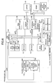
- Fig.1 is a block diagram of a processor according to the first embodiment of the present invention.
- a processor 10 of Fig.1 includes a clock control unit 11, a CPU core unit 12, a DSP core unit 13, a module 14, a module 15, a bus bridge 16 connecting between an on-chip bus (OCB) and a built-in peripheral bus (PB), a DMA controller 17, an SDRAM controller 18, an external bus controller 19, a bus arbiter 20 for the on-chip bus, the on-chip bus (OCB) 21, modules 22 through 24, the internal peripheral bus (PB) 25, an SRAM 26 and an external bus master chip 27 provided outside the processor 10 and connected to the external bus controller 19, an external bus 28, and an SDRAM 29 provided outside the processor 10 and connected to the SDRAM controller 18.
- a clock control unit 11 includes a clock control unit 11, a CPU core unit 12, a DSP core unit 13, a module 14, a module 15, a bus bridge 16 connecting between an on-chip bus (OCB) and a built-in peripheral bus (PB), a DMA controller 17, an SDRAM controller 18, an external bus controller 19, a bus arbiter 20 for the on-chip bus,
- the CPU core unit 12, the DSP core unit 13, the module 14, the module 15, the DMA controller 17, the SDRAM controller 18, and the external bus controller 19 are on-chip bus modules connected to the on-chip bus 21.
- the modules 22 through 24 are peripheral-bus modules connected to the internal peripheral bus 25.
- the SRAM 26 and the external bus master chip 27 are external-bus modules connected to the external bus 28.
- the clock control unit 11 includes a clock generation unit. 30 and a clock control check unit 31.
- the module 22 includes a clock control register 32.
- clock control a gear shift or a transition to the power-down mode
- a store (write) instruction is issued so as to store clock-control request data in the clock control register 32 of the module 22 connected to the internal peripheral bus 25.
- the write data of this store instruction is provided from the CPU core unit 12, and is transferred to the bus bridge 16 according to the transfer protocols of the on-chip bus 21. Further, the bus bridge 16 transmits a write request regarding the write data to the module 22, resulting in the write data being stored in the clock control register 32 of the module 22.
- the CPU core unit 12 executes subsequent instructions successively on a pipeline basis after issuing the store instruction for storing the clock-control request data.
- the clock control register 32 When the clock-control request data is stored in the clock control register 32, the clock control register 32 sends a clock-control demand signal to the clock control unit 11.
- the clock-control demand signal is received by the clock control check unit 31 of the clock control unit 11. Having found that the clock-control demand signal is asserted, the clock control check unit 31 asserts a clock-control request signal req to each module that is subjected to clock control.
- the clock-control request signal req is maintained in an asserting state until a clock-control-completion notifying signal DN is asserted.
- Modules that receive the clock-control request signal req and assert the clock-control acknowledge signal includes the bus arbiter 20, the CPU core unit 12, the DSP core unit 13, the DMA controller 17, the SDRAM controller 18, the external bus controller 19, and the bus bridge 16.
- the bus arbiter 20 arbitrates the bus right (i.e., the right to use the bus) between the modules connected to the on-chip. bus 21, and permits access to the bus by granting the bus right to a selected module.
- the bus bridge 16 performs data transfer between the on-chip bus 21 and the internal peripheral bus 25.
- the clock-control acknowledge signal ack0 is maintained in the asserted condition until the clock-control request signal req is negated.
- the clock control check unit 31 learns this fact, and asserts a clock-control enable signal EN against the clock generation unit 30. At this point of time, all the modules subjected to clock control are temporarily suspending an operation thereof.
- the clock generation unit 30 Upon detecting the clock-control enable signal EN, the clock generation unit 30 carries out a clock-control operation such as a clock-gear shift or a transition to the power-down mode requested by a program. Details of the clock-control operation are specified in the contents of the clock-control request data stored in the clock control register 32.
- the clock generation unit 30 is a source of clock signals that are supplied to the relevant modules. According to the request made by the program, the clock generation unit 30 selectively controls clock signals supplied to respective modules, thereby changing the operation frequency and/or suspending the supply of a clock signal on a module-specific basis.
- the clock generation unit 30 asserts a clock-control-completion notifying signal DN when the clock control process comes to an end.
- the clock control check unit 31 negates the clock-control request signal req.
- each clock-control-subjected module negates the clock-control acknowledge signal ackx.
- the clock-control enable signal EN is negated, followed by the clock-control-completion notifying signal DN being negated.
- Fig.2 is a timing chart showing signals described above.
- the bus grant signal gntx is negated in response as shown in Fig.2-(b).
- the clock-control acknowledge signals ackx from the respective modules are changed to HIGH (in the asserted condition) as shown in Fig.2-(c) through (j).
- the clock-control enable signal EN turns to HIGH as shown in Fig.2-(k), which initiates a clock-control operation such as a clock-gear shift or a clock suspension.
- the clock-control-completion notifying signal DN is asserted.
- the present invention insures that clock control is carried out only after eliminating all the risks of having malfunctions by suspending all the modules having the risks of irregular operations caused by such clock control.
- Fig.3 is a block diagram showing an example configuration of the clock control check unit 31.
- the clock control check unit 31 of Fig.3 includes a flip-flop 41, flip-flops 42-0 through 42-6, a clock-control decoder circuit 43, an AND circuit 44, and a request signal generation circuit 45.
- the flip-flop 41 latches the clock-control demand signal supplied from the clock control register 32.
- the latched clock-control demand signal is supplied to the clock-control decoder circuit 43, and is decoded thereby.
- the clock-control demand signal is comprised of a plurality of bits, and requests clock control.
- the clock-control demand signal specifies the details of control in a specific manner, for example, regarding whether the clock control is directed to a clock-gear shift or a clock suspension, which modules are subjected to the clock control, etc.
- the clock-control decoder circuit 43 decodes the clock-control demand signal, and generates control signals CTL for performing the specified clock control operations, followed by supplying the control signals CTL to the clock generation unit 30. Furthermore, the clock control decoder circuit 43 supplies a signal clk_ctr indicative of clock control to the request signal generation circuit 45.
- the request signal generation circuit 45 is a simple state machine, and switches between an idle state IDLE and a clock-control state CLK_CTRL according to the incoming signal.
- the request signal generation circuit 45 shifts from the idle state IDLE to the clock-control state CLK_CTRL, and asserts the clock-control request signal req.
- the clock-control-completion notifying signal DN is asserted, the write-signal selector 45 switches from the clock-control state CLK_CTRL to the idle state IDLE, and negates the clock-control request signal req.
- the request signal generation circuit 45 could be made by use of simple sequential logic circuits such as set-reset flip-flops.
- the AND circuit 44 performs an AND operation so as to assert the clock-control enable signal EN in response to the asserted statuses of all the clock-control acknowledge signals.
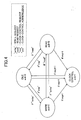
- Fig.4 is a drawing showing a clock-control mechanism used in the bus bridge 16 that is subjected to clock control.
- the clock-control mechanism of Fig.4 is a simple state machine that makes a state transition in response to an incoming signal, and has four transition states, which include a clock-control state, a write-in state WRITE, a read-out state READ, and an idle state IDLE.
- the bus bridge 16 waits for an operation instruction to come.
- the bus bridge 16 switches to the write-in state WRITE or to the read-out state READ according to the arrived request.
- the write-in state WRITE a process is performed that receives data from the on-chip bus 21 and writes the data in the module of the internal peripheral bus 25.
- the read-out state READ a process is performed that reads data from the module of the internal peripheral bus 25 and supplies the data to the on-chip bus 21.
- the bus bridge 16 When the a clock-control request signal req is asserted while one of the write-in state WRITE, the read-out state READ, and the idle-state IDLE is engaged, the bus bridge 16 will moves into the clock control state. Moving into the clock control state, the bus bridge 16 performs operations necessary as preparations for a clock-gear shift or a clock suspension, and asserts the clock-control acknowledge signal ack (ack6 in Fig.1) when these operations are completed. Namely, the bus bridge 16 completes the currently performed operation, suspends processing, and asserts the clock-control acknowledge signal ack (ack6 in Fig.1). When the clock-control request signal req is negated thereafter, the state-is changed to the idle state IDLE.
- the state machine performing operations as described above could be made by use of simple sequential logic circuits such as set-reset flip-flops.
- Each of the modules that are subjected to clock control in Fig.1 is provided with substantially the same state machine that is shown in Fig.4, and is configured to assert the clock-control acknowledge signal ack after completing a preparatory operation for a clock shift or a clock suspension in response to the assertion of the clock-control request signal req.
- Fig.5 is a block diagram of a processor according to the second embodiment of the present invention.
- the same elements as those of Fig.1 are. referred by the same numerals.
- a clock control unit 11A is provided in place of the clock control unit 11, and a CPU core unit 12A is provided instead of the CPU core unit 12. Further, a module 22A is provided in place of a module 22.
- the second embodiment differs from the first embodiment in terms of its configuration and operation in that the clock control register 32 is situated in the CPU core unit 12A, and in that the CPU core unit 12A generates the clock-control request signal req, and supplies same to each unit.
- the CPU core unit 12A asserts the clock-control request signal req.
- relevant modules suspend operations thereof after currently performed operations come to an end, and change the clock-control acknowledge signals ackx to HIGH (asserted condition).
- the clock control unit 11A changes the clock-control enable signal EN to HIGH when all the clock-control acknowledge signals ackx become HIGH. This initiates a clock-control operation such as a clock-gear shift or a clock suspension.
- the. clock-control-completion notifying signal DN is asserted.
- the second embodiment is basically the same as the first embodiment, except that the CPU core unit 12A asserts the clock-control request signal req.
- Fig.6 is a block diagram of a processor according to a third embodiment of the present invention.
- the same elements as those of Fig.1 are referred to by the same numerals.
- the clock-control request signal req asserted by a clock control check unit 31B of a clock control unit 11B is supplied only to the bus arbiter 20.
- no clock-control request signal req is supplied to a CPU core unit 12B, a DSP core unit 13B, a bus bridge 16B, a DMA controller 17B, an SDRAM controller 18B, and an external bus controller 19B.
- the configuration of the third embodiment described above is particularly effective where transactions via the on-chip bus 21 are the only possible source of problems when clock control is carried out to make a clock-gear shift or a transition to the power-down mode.
- the clock-control request signal req may be supplied exclusively to the bus arbiter 20 so as to suspend operations of the bus masters connected to the on-chip bus 21 through control of the bus grant signals, thereby suspending transactions through the on-chip bus 21 prior to the commencement of clock control.
- the configuration of the third embodiment can reduce the circuit size by reducing the number of modules that are controlled by way of the clock-control request signal req.
- Fig.7 is a block diagram showing a processor according to the fourth embodiment of the present invention.
- the same elements as those of Fig.6 are referred to by the same numerals.
- the clock-control request signal req asserted by a clock control check unit 31C of a clock control unit 11C is supplied only to the bus arbiter 20 and the bus bridge 16.
- the modules connected to the on-chip bus 21, except for the bus bridge 16 do not cause problems if the bus arbiter 20 refuses to grant the bus right by use of bus-grant signals. Accordingly, the clock-control request signal req is not supplied to the CPU core unit 12B, the DSP core unit 13B, the DMA controller 17B, the SDRAM controller 18B, and the external bus controller 19B.
- the bus bridge 16 After receiving the clock-control request signal req, the bus bridge 16 stops writing data from the on-chip bus 21 to a module of the internal peripheral bus 25 or stops reading data from a module of the internal peripheral bus 25 to the on-chip bus 21 when a currently performed data transfer transaction is completed. Thereafter, the bus bridge 16 asserts the clock-control acknowledge signal ack6.
- the configuration of the fourth embodiment described above is particularly effective where transactions on the on-chip bus 21 and data transfer via the bus bridge 16 are the only possible source of problems when clock control is carried out to make a clock-gear shift or a transition to the power-down mode.
- the clock-control request signal req may be supplied exclusively to the bus arbiter 20 and the bus bridge 16 so as to suspend the operations of the bus masters connected to the on-chip bus 21 through control of the bus grant signals and to suspend the operation of the bus bridge 16, thereby suspending all the transactions possibly causing problems prior to the commencement of clock control.
- the configuration of the fourth embodiment can reduce the circuit size by reducing the number of modules that are controlled by way of the clock-control request signal req.
Landscapes
- Engineering & Computer Science (AREA)
- Theoretical Computer Science (AREA)
- Physics & Mathematics (AREA)
- General Engineering & Computer Science (AREA)
- General Physics & Mathematics (AREA)
- Information Transfer Systems (AREA)
- Executing Machine-Instructions (AREA)
- Bus Control (AREA)
- Microcomputers (AREA)
- Power Sources (AREA)
- Tests Of Electronic Circuits (AREA)
Abstract
Description
Claims (10)
- A semiconductor device, comprising:wherein said clock generation unit selectively changes the clock signal supplied to said one or plurality of second modules in response to assertion of all the clock-control acknowledge signals output from said one or plurality of second modules.a clock generation unit which generates a clock signal;a first module which asserts a clock-control request signal; andone or a plurality of second modules, each of which receives the clock signal and the clock-control request signal, and asserts a clock-control acknowledge signal after stopping an operation thereof upon completion of a currently performed operation in response to the assertion of the clock-control request signal,
- The semiconductor device as claimed in claim 1, wherein said clock generation unit selectively changes the clock signal by changing a frequency of the clock signal or stopping supply of the clock signal supplied to said one or plurality of second modules.
- The semiconductor device as claimed in claim 1, wherein said first module is a CPU core circuit.
- The semiconductor device as claimed in claim 1, wherein said first module asserts a clock-control enable signal to said clock generation unit in response to the assertion of all the clock-control acknowledge signals output from said one or plurality of second modules, and said clock generation unit selectively changes the clock signal in response to the assertion of the clock-control enable signal.
- The semiconductor device as claimed in claim 1, further comprising:a on-chip bus;a plurality of modules connected to said on-chip bus; anda bus arbiter which arbitrates a bus right between bus masters that are some of said plurality of modules, wherein said bus arbiter is one of said one or plurality of second modules, and asserts the clock-control acknowledge signal after refusing to grant the bus right to any one of the bus masters upon completion of a currently performed transfer operation on said on-chip bus in response to the assertion of the clock-control request signal.
- The semiconductor device as claimed in claim 5, wherein said one or plurality of second modules consists of said bus arbiter.
- The semiconductor device as claimed in claim 5, further comprising:wherein said bus bridge is one of said one or plurality of second modules, and asserts the clock-control acknowledge signal after refraining from performing a data transfer operation upon completion of a currently performed data transfer operation on said internal peripheral bus in response to the assertion of the clock-control request signal.an internal peripheral bus; anda bus bridge which connects between said internal peripheral bus and said on-chip bus,
- The semiconductor device as claimed in claim 7, wherein said one or plurality of second modules consists of said bus arbiter and said bus bridge.
- A method of selectively controlling a clock signal supplied to each module in a processor, comprising the steps of:asserting a clock-control request signal to one or a plurality of modules;asserting a clock-control acknowledge signal from each of said one or plurality of modules after stopping an operation thereof upon completion of a currently performed operation in response to the assertion of the clock-control request signal; andselectively changing a clock signal supplied to said one or plurality of modules in response to assertion of all the clock-control acknowledge signals output from said one or plurality of modules.
- The method as claimed in claim 9, wherein said step of selectively changing the clock signal changes a frequency of the clock signal or stops supply of the clock signal supplied to the said one or plurality of modules.
Applications Claiming Priority (2)
| Application Number | Priority Date | Filing Date | Title |
|---|---|---|---|
| JP2001246654 | 2001-08-15 | ||
| JP2001246654A JP4733877B2 (en) | 2001-08-15 | 2001-08-15 | Semiconductor device |
Publications (3)
| Publication Number | Publication Date |
|---|---|
| EP1286248A2 true EP1286248A2 (en) | 2003-02-26 |
| EP1286248A3 EP1286248A3 (en) | 2003-08-27 |
| EP1286248B1 EP1286248B1 (en) | 2005-11-09 |
Family
ID=19076156
Family Applications (1)
| Application Number | Title | Priority Date | Filing Date |
|---|---|---|---|
| EP02251299A Expired - Lifetime EP1286248B1 (en) | 2001-08-15 | 2002-02-25 | Semiconductor device with hardware mechanism for proper clock control |
Country Status (5)
| Country | Link |
|---|---|
| US (1) | US7093152B2 (en) |
| EP (1) | EP1286248B1 (en) |
| JP (1) | JP4733877B2 (en) |
| CN (2) | CN1402100A (en) |
| DE (1) | DE60207161T2 (en) |
Cited By (5)
| Publication number | Priority date | Publication date | Assignee | Title |
|---|---|---|---|---|
| WO2006028652A3 (en) * | 2004-09-03 | 2006-07-06 | Intel Corp | Coordinating idle state transitions in multi-core processors |
| US7076672B2 (en) | 2002-10-14 | 2006-07-11 | Intel Corporation | Method and apparatus for performance effective power throttling |
| US7237128B2 (en) | 2002-10-14 | 2007-06-26 | Intel Corporation | Method and apparatus to dynamically change an operating frequency and operating voltage of an electronic device |
| US7664970B2 (en) | 2005-12-30 | 2010-02-16 | Intel Corporation | Method and apparatus for a zero voltage processor sleep state |
| US7966511B2 (en) | 2004-07-27 | 2011-06-21 | Intel Corporation | Power management coordination in multi-core processors |
Families Citing this family (49)
| Publication number | Priority date | Publication date | Assignee | Title |
|---|---|---|---|---|
| US6760772B2 (en) | 2000-12-15 | 2004-07-06 | Qualcomm, Inc. | Generating and implementing a communication protocol and interface for high data rate signal transfer |
| US8812706B1 (en) | 2001-09-06 | 2014-08-19 | Qualcomm Incorporated | Method and apparatus for compensating for mismatched delays in signals of a mobile display interface (MDDI) system |
| DE10303673A1 (en) * | 2003-01-24 | 2004-08-12 | IHP GmbH - Innovations for High Performance Microelectronics/Institut für innovative Mikroelektronik | Asynchronous envelope for a globally asynchronous, locally synchronous (GALS) circuit |
| ATE517500T1 (en) | 2003-06-02 | 2011-08-15 | Qualcomm Inc | GENERATION AND IMPLEMENTATION OF A SIGNAL PROTOCOL AND INTERFACE FOR HIGHER DATA RATES |
| DE602004000260T2 (en) | 2003-07-22 | 2006-08-24 | Arena Pharmaceuticals, Inc., San Diego | DIARYL AND ARYLHETEROARYL DRUG DERIVATIVES AS MODULATORS OF THE 5-HT2A SEROTONIN RECEPTOR SUITABLE FOR THE PROPHYLAXIS AND TREATMENT OF RELATED DISEASES THEREOF |
| JP4136822B2 (en) | 2003-07-31 | 2008-08-20 | 富士通株式会社 | Semiconductor integrated circuit device, clock control method, and data transfer control method |
| AU2004300958A1 (en) | 2003-08-13 | 2005-02-24 | Qualcomm, Incorporated | A signal interface for higher data rates |
| KR100951158B1 (en) | 2003-09-10 | 2010-04-06 | 콸콤 인코포레이티드 | High-speed data interface |
| US7640446B1 (en) | 2003-09-29 | 2009-12-29 | Marvell International Ltd. | System-on-chip power reduction through dynamic clock frequency |
| EP1680904A1 (en) | 2003-10-15 | 2006-07-19 | QUALCOMM Incorporated | High data rate interface |
| TWI401601B (en) | 2003-10-29 | 2013-07-11 | Qualcomm Inc | Method and system for a mobile display digital interface system and computer program product |
| CN101729205A (en) | 2003-11-12 | 2010-06-09 | 高通股份有限公司 | High data rate interface with improved link control |
| RU2006122542A (en) | 2003-11-25 | 2008-01-10 | Квэлкомм Инкорпорейтед (US) | HIGH-SPEED DATA TRANSFER INTERFACE WITH IMPROVED COMMUNICATION LINK SYNCHRONIZATION |
| CA2731269C (en) | 2003-12-08 | 2013-01-08 | Qualcomm Incorporated | High data rate interface with improved link synchronization |
| EP2309695A1 (en) | 2004-03-10 | 2011-04-13 | Qualcomm Incorporated | High data rate interface apparatus and method |
| WO2005091593A1 (en) | 2004-03-17 | 2005-09-29 | Qualcomm Incorporated | High data rate interface apparatus and method |
| US8645566B2 (en) | 2004-03-24 | 2014-02-04 | Qualcomm Incorporated | High data rate interface apparatus and method |
| US8650304B2 (en) | 2004-06-04 | 2014-02-11 | Qualcomm Incorporated | Determining a pre skew and post skew calibration data rate in a mobile display digital interface (MDDI) communication system |
| AU2005253592B2 (en) | 2004-06-04 | 2009-02-05 | Qualcomm Incorporated | High data rate interface apparatus and method |
| US8723705B2 (en) | 2004-11-24 | 2014-05-13 | Qualcomm Incorporated | Low output skew double data rate serial encoder |
| US8667363B2 (en) | 2004-11-24 | 2014-03-04 | Qualcomm Incorporated | Systems and methods for implementing cyclic redundancy checks |
| US8539119B2 (en) | 2004-11-24 | 2013-09-17 | Qualcomm Incorporated | Methods and apparatus for exchanging messages having a digital data interface device message format |
| US8873584B2 (en) | 2004-11-24 | 2014-10-28 | Qualcomm Incorporated | Digital data interface device |
| US8692838B2 (en) | 2004-11-24 | 2014-04-08 | Qualcomm Incorporated | Methods and systems for updating a buffer |
| US8699330B2 (en) | 2004-11-24 | 2014-04-15 | Qualcomm Incorporated | Systems and methods for digital data transmission rate control |
| US7725759B2 (en) * | 2005-06-29 | 2010-05-25 | Sigmatel, Inc. | System and method of managing clock speed in an electronic device |
| US8692839B2 (en) | 2005-11-23 | 2014-04-08 | Qualcomm Incorporated | Methods and systems for updating a buffer |
| US8730069B2 (en) | 2005-11-23 | 2014-05-20 | Qualcomm Incorporated | Double data rate serial encoder |
| TWI415845B (en) | 2006-10-03 | 2013-11-21 | Arena Pharm Inc | Pyrazole derivatives as modulators of the 5-ht2a serotonin receptor useful for the treatment of disorders related thereto |
| JP5393677B2 (en) | 2007-08-15 | 2014-01-22 | アリーナ ファーマシューティカルズ, インコーポレイテッド | Imidazo [1,2-a] pyridine derivatives as modulators of 5-HT2A serotonin receptors for the treatment of disorders associated with 5-HT2A serotonin receptors |
| JP2009122922A (en) * | 2007-11-14 | 2009-06-04 | Panasonic Corp | Data processor |
| US20110021538A1 (en) | 2008-04-02 | 2011-01-27 | Arena Pharmaceuticals, Inc. | Processes for the preparation of pyrazole derivatives useful as modulators of the 5-ht2a serotonin receptor |
| CA2741731A1 (en) | 2008-10-28 | 2010-06-03 | Arena Pharmaceuticals, Inc. | Compositions of a 5-ht2a serotonin receptor modulator useful for the treatment of disorders related thereto |
| US9126946B2 (en) | 2008-10-28 | 2015-09-08 | Arena Pharmaceuticals, Inc. | Processes useful for the preparation of 1-[3-(4-bromo-2-methyl-2H-pyrazol-3-yl)-4-methoxy-phenyl]-3-(2,4-difluoro-phenyl)urea and crystalline forms related thereto |
| JP2011223179A (en) | 2010-04-07 | 2011-11-04 | Renesas Electronics Corp | Clock generation circuit and control method of the same |
| JP5751819B2 (en) | 2010-12-16 | 2015-07-22 | キヤノン株式会社 | Data processing apparatus, data processing method, and program |
| WO2012157033A1 (en) * | 2011-05-17 | 2012-11-22 | パナソニック株式会社 | Stream processing device |
| JP2013106166A (en) * | 2011-11-14 | 2013-05-30 | Sony Corp | Clock gating circuit and bus system |
| KR101975409B1 (en) | 2012-07-26 | 2019-05-08 | 삼성전자주식회사 | System on chip and temperature control method thereof |
| JP6774160B2 (en) | 2013-12-06 | 2020-10-21 | キヤノン株式会社 | Information processing device and data transfer device control method |
| CN103746691B (en) * | 2014-01-23 | 2017-01-11 | 海信集团有限公司 | Clock signal control system and method |
| CN104076863B (en) * | 2014-07-01 | 2017-03-01 | 大唐微电子技术有限公司 | A kind of clock switching device |
| JP6425492B2 (en) | 2014-10-17 | 2018-11-21 | キヤノン株式会社 | INFORMATION PROCESSING APPARATUS, INFORMATION PROCESSING METHOD, AND PROGRAM |
| US10022355B2 (en) | 2015-06-12 | 2018-07-17 | Axovant Sciences Gmbh | Diaryl and arylheteroaryl urea derivatives as modulators of the 5-HT2A serotonin receptor useful for the prophylaxis and treatment of REM sleep behavior disorder |
| BR112018000728A2 (en) | 2015-07-15 | 2018-09-04 | Axovant Sciences Gmbh | method for the prophylaxis and / or treatment of visual hallucinations in a subject in need |
| JP5981004B2 (en) * | 2015-09-02 | 2016-08-31 | ルネサスエレクトロニクス株式会社 | Semiconductor device |
| US11867744B2 (en) * | 2020-10-20 | 2024-01-09 | Nvidia Corporation | Techniques for isolating interfaces while testing semiconductor devices |
| JP2023009676A (en) | 2021-07-07 | 2023-01-20 | キヤノン株式会社 | Arithmetic processing unit and control method thereof |
| WO2025120727A1 (en) * | 2023-12-05 | 2025-06-12 | 三菱電機株式会社 | Control circuit for asynchronous circuit, and asynchronous circuit |
Family Cites Families (19)
| Publication number | Priority date | Publication date | Assignee | Title |
|---|---|---|---|---|
| JPH0528116A (en) * | 1991-07-22 | 1993-02-05 | Sharp Corp | Multi-processor system |
| US5452401A (en) | 1992-03-31 | 1995-09-19 | Seiko Epson Corporation | Selective power-down for high performance CPU/system |
| JPH0683616A (en) | 1992-09-02 | 1994-03-25 | Mitsubishi Denki Enjiniriangu Kk | Semiconductor integrated circuit |
| US5376928A (en) * | 1992-09-18 | 1994-12-27 | Thomson Consumer Electronics, Inc. | Exchanging data and clock lines on multiple format data buses |
| US5600839A (en) | 1993-10-01 | 1997-02-04 | Advanced Micro Devices, Inc. | System and method for controlling assertion of a peripheral bus clock signal through a slave device |
| EP0644475B1 (en) | 1993-09-22 | 2004-07-21 | Advanced Micro Devices, Inc. | Apparatus and method for controlling a peripheral bus clock signal |
| US6163848A (en) | 1993-09-22 | 2000-12-19 | Advanced Micro Devices, Inc. | System and method for re-starting a peripheral bus clock signal and requesting mastership of a peripheral bus |
| US5471625A (en) | 1993-09-27 | 1995-11-28 | Motorola, Inc. | Method and apparatus for entering a low-power mode and controlling an external bus of a data processing system during low-power mode |
| ATE231254T1 (en) | 1994-04-28 | 2003-02-15 | Advanced Micro Devices Inc | SYSTEM FOR CONTROLLING A PERIPHERAL BUST CLOCK SIGNAL |
| US5517650A (en) | 1994-12-19 | 1996-05-14 | International Business Machines Corporation | Bridge for a power managed computer system with multiple buses and system arbitration |
| JPH0997128A (en) * | 1995-09-26 | 1997-04-08 | Internatl Business Mach Corp <Ibm> | Information-processing system |
| JPH09212479A (en) * | 1996-02-07 | 1997-08-15 | Hitachi Ltd | Single chip microcomputer |
| JP2822986B2 (en) * | 1996-06-28 | 1998-11-11 | 日本電気株式会社 | Single chip microcomputer with DMA |
| JP2000020462A (en) * | 1998-06-30 | 2000-01-21 | Toshiba Corp | Bus system applied to computer system |
| US6088806A (en) * | 1998-10-20 | 2000-07-11 | Seiko Epson Corporation | Apparatus and method with improved power-down mode |
| US6754826B1 (en) * | 1999-03-31 | 2004-06-22 | International Business Machines Corporation | Data processing system and method including a network access connector for limiting access to the network |
| US6678281B1 (en) * | 2000-03-08 | 2004-01-13 | Lucent Technologies Inc. | Hardware configuration, support node and method for implementing general packet radio services over GSM |
| US6748546B1 (en) * | 2000-09-26 | 2004-06-08 | Sun Microsystems, Inc. | Method and apparatus for reducing power consumption |
| US6735653B2 (en) * | 2001-02-16 | 2004-05-11 | Koninklijke Philips Electronics N.V. | Bus bandwidth consumption profiler |
-
2001
- 2001-08-15 JP JP2001246654A patent/JP4733877B2/en not_active Expired - Fee Related
-
2002
- 2002-02-22 US US10/079,903 patent/US7093152B2/en not_active Expired - Lifetime
- 2002-02-25 DE DE60207161T patent/DE60207161T2/en not_active Expired - Lifetime
- 2002-02-25 EP EP02251299A patent/EP1286248B1/en not_active Expired - Lifetime
- 2002-03-19 CN CN02107584A patent/CN1402100A/en active Pending
- 2002-03-19 CN CNB2005100666738A patent/CN100347642C/en not_active Expired - Lifetime
Cited By (17)
| Publication number | Priority date | Publication date | Assignee | Title |
|---|---|---|---|---|
| US7237128B2 (en) | 2002-10-14 | 2007-06-26 | Intel Corporation | Method and apparatus to dynamically change an operating frequency and operating voltage of an electronic device |
| US7076672B2 (en) | 2002-10-14 | 2006-07-11 | Intel Corporation | Method and apparatus for performance effective power throttling |
| US8726048B2 (en) | 2004-07-27 | 2014-05-13 | Intel Corporation | Power management coordination in multi-core processors |
| US9870044B2 (en) | 2004-07-27 | 2018-01-16 | Intel Corporation | Method and apparatus for a zero voltage processor sleep state |
| US7966511B2 (en) | 2004-07-27 | 2011-06-21 | Intel Corporation | Power management coordination in multi-core processors |
| US9841807B2 (en) | 2004-07-27 | 2017-12-12 | Intel Corporation | Method and apparatus for a zero voltage processor sleep state |
| US9235258B2 (en) | 2004-07-27 | 2016-01-12 | Intel Corporation | Method and apparatus for a zero voltage processor |
| US9081575B2 (en) | 2004-07-27 | 2015-07-14 | Intel Corporation | Method and apparatus for a zero voltage processor sleep state |
| US9141180B2 (en) | 2004-07-27 | 2015-09-22 | Intel Corporation | Method and apparatus for a zero voltage processor sleep state |
| US9223389B2 (en) | 2004-07-27 | 2015-12-29 | Intel Corporation | Method and apparatus for a zero voltage processor |
| US9223390B2 (en) | 2004-07-27 | 2015-12-29 | Intel Corporation | Method and apparatus for a zero voltage processor |
| US7451333B2 (en) | 2004-09-03 | 2008-11-11 | Intel Corporation | Coordinating idle state transitions in multi-core processors |
| WO2006028652A3 (en) * | 2004-09-03 | 2006-07-06 | Intel Corp | Coordinating idle state transitions in multi-core processors |
| CN101010655B (en) * | 2004-09-03 | 2010-05-26 | 英特尔公司 | Coordinating idle state transitions in a multi-core processor |
| US7664970B2 (en) | 2005-12-30 | 2010-02-16 | Intel Corporation | Method and apparatus for a zero voltage processor sleep state |
| US8707066B2 (en) | 2005-12-30 | 2014-04-22 | Intel Corporation | Method and apparatus for a zero voltage processor sleep state |
| US7953993B2 (en) | 2005-12-30 | 2011-05-31 | Intel Corporation | Method and apparatus for a zero voltage processor sleep state |
Also Published As
| Publication number | Publication date |
|---|---|
| US20030037274A1 (en) | 2003-02-20 |
| CN100347642C (en) | 2007-11-07 |
| CN1402100A (en) | 2003-03-12 |
| DE60207161D1 (en) | 2005-12-15 |
| DE60207161T2 (en) | 2006-06-14 |
| CN1670668A (en) | 2005-09-21 |
| US7093152B2 (en) | 2006-08-15 |
| EP1286248A3 (en) | 2003-08-27 |
| JP4733877B2 (en) | 2011-07-27 |
| JP2003058271A (en) | 2003-02-28 |
| EP1286248B1 (en) | 2005-11-09 |
Similar Documents
| Publication | Publication Date | Title |
|---|---|---|
| EP1286248B1 (en) | Semiconductor device with hardware mechanism for proper clock control | |
| JP3526920B2 (en) | Computer system and system and method for controlling peripheral bus clock signals | |
| US5471625A (en) | Method and apparatus for entering a low-power mode and controlling an external bus of a data processing system during low-power mode | |
| US11487684B2 (en) | Power management in a seamlessly integrated microcontroller chip | |
| TWI437434B (en) | Direct memory access controller | |
| TWI443519B (en) | System for direct memory access, method for performing a data transmission, and microcontroller | |
| US8531893B2 (en) | Semiconductor device and data processor | |
| JP3633998B2 (en) | Computer system | |
| JPH0157811B2 (en) | ||
| US6883102B2 (en) | Apparatus and method for performing power management functions | |
| KR20040091705A (en) | Low power system and method for a data processing system | |
| JP3638271B2 (en) | Information processing device | |
| US7290158B2 (en) | Method of controlling data transfer within a semiconductor integrated circuit based on a clock sync control signal | |
| US5974479A (en) | System for executing, canceling, or suspending a DMA transfer based upon internal priority comparison between a DMA transfer and an interrupt request | |
| EP0644475B1 (en) | Apparatus and method for controlling a peripheral bus clock signal | |
| US20090125738A1 (en) | Data processing apparatus | |
| US8645602B2 (en) | Microcomputer | |
| WO2002093392A1 (en) | Data processor | |
| JP3120203B2 (en) | Soft timer | |
| JP2001184305A (en) | External bus controller | |
| JP2002373145A (en) | Direct memory access device | |
| JPH07182272A (en) | Dma controller circuit | |
| JPH05204826A (en) | Data processing device | |
| JPH11328111A (en) | Clock synchronous bus circuit | |
| JP2006065444A (en) | Semiconductor integrated circuit and data processor |
Legal Events
| Date | Code | Title | Description |
|---|---|---|---|
| PUAI | Public reference made under article 153(3) epc to a published international application that has entered the european phase |
Free format text: ORIGINAL CODE: 0009012 |
|
| AK | Designated contracting states |
Kind code of ref document: A2 Designated state(s): AT BE CH CY DE DK ES FI FR GB GR IE IT LI LU MC NL PT SE TR |
|
| AX | Request for extension of the european patent |
Extension state: AL LT LV MK RO SI |
|
| PUAL | Search report despatched |
Free format text: ORIGINAL CODE: 0009013 |
|
| AK | Designated contracting states |
Designated state(s): AT BE CH CY DE DK ES FI FR GB GR IE IT LI LU MC NL PT SE TR |
|
| AX | Request for extension of the european patent |
Extension state: AL LT LV MK RO SI |
|
| 17P | Request for examination filed |
Effective date: 20040211 |
|
| 17Q | First examination report despatched |
Effective date: 20040406 |
|
| AKX | Designation fees paid |
Designated state(s): DE FR GB |
|
| GRAP | Despatch of communication of intention to grant a patent |
Free format text: ORIGINAL CODE: EPIDOSNIGR1 |
|
| RIN1 | Information on inventor provided before grant (corrected) |
Inventor name: HIJI, YOSHIHIRO,C/O FUJITSU LIMITED Inventor name: HIRATA, TAKUYA,C/O FUJITSU LIMITED Inventor name: SATOH, TAIZOH,C/O FUJITSU LIMITED Inventor name: SHIKATA, TAKASHI,C/O FUJITSU LIMITED |
|
| GRAS | Grant fee paid |
Free format text: ORIGINAL CODE: EPIDOSNIGR3 |
|
| GRAA | (expected) grant |
Free format text: ORIGINAL CODE: 0009210 |
|
| AK | Designated contracting states |
Kind code of ref document: B1 Designated state(s): DE FR GB |
|
| REG | Reference to a national code |
Ref country code: GB Ref legal event code: FG4D |
|
| REF | Corresponds to: |
Ref document number: 60207161 Country of ref document: DE Date of ref document: 20051215 Kind code of ref document: P |
|
| ET | Fr: translation filed | ||
| PLBE | No opposition filed within time limit |
Free format text: ORIGINAL CODE: 0009261 |
|
| STAA | Information on the status of an ep patent application or granted ep patent |
Free format text: STATUS: NO OPPOSITION FILED WITHIN TIME LIMIT |
|
| 26N | No opposition filed |
Effective date: 20060810 |
|
| REG | Reference to a national code |
Ref country code: GB Ref legal event code: 732E |
|
| REG | Reference to a national code |
Ref country code: FR Ref legal event code: TP |
|
| PGFP | Annual fee paid to national office [announced via postgrant information from national office to epo] |
Ref country code: FR Payment date: 20090213 Year of fee payment: 8 |
|
| PGFP | Annual fee paid to national office [announced via postgrant information from national office to epo] |
Ref country code: GB Payment date: 20100202 Year of fee payment: 9 |
|
| REG | Reference to a national code |
Ref country code: FR Ref legal event code: ST Effective date: 20101029 |
|
| PG25 | Lapsed in a contracting state [announced via postgrant information from national office to epo] |
Ref country code: FR Free format text: LAPSE BECAUSE OF NON-PAYMENT OF DUE FEES Effective date: 20100301 |
|
| GBPC | Gb: european patent ceased through non-payment of renewal fee |
Effective date: 20110225 |
|
| PG25 | Lapsed in a contracting state [announced via postgrant information from national office to epo] |
Ref country code: GB Free format text: LAPSE BECAUSE OF NON-PAYMENT OF DUE FEES Effective date: 20110225 |
|
| REG | Reference to a national code |
Ref country code: DE Ref legal event code: R082 Ref document number: 60207161 Country of ref document: DE Representative=s name: REICHERT & LINDNER PARTNERSCHAFT PATENTANWAELT, DE |
|
| REG | Reference to a national code |
Ref country code: DE Ref legal event code: R082 Ref document number: 60207161 Country of ref document: DE Representative=s name: REICHERT & LINDNER PARTNERSCHAFT PATENTANWAELT, DE Effective date: 20150512 Ref country code: DE Ref legal event code: R081 Ref document number: 60207161 Country of ref document: DE Owner name: SOCIONEXT INC., YOKOHAMA-SHI, JP Free format text: FORMER OWNER: FUJITSU SEMICONDUCTOR LTD., YOKOHAMA, KANAGAWA, JP Effective date: 20150512 |
|
| PGFP | Annual fee paid to national office [announced via postgrant information from national office to epo] |
Ref country code: DE Payment date: 20210217 Year of fee payment: 20 |
|
| REG | Reference to a national code |
Ref country code: DE Ref legal event code: R071 Ref document number: 60207161 Country of ref document: DE |