JP3633998B2 - Computer system - Google Patents
Computer system Download PDFInfo
- Publication number
- JP3633998B2 JP3633998B2 JP10408695A JP10408695A JP3633998B2 JP 3633998 B2 JP3633998 B2 JP 3633998B2 JP 10408695 A JP10408695 A JP 10408695A JP 10408695 A JP10408695 A JP 10408695A JP 3633998 B2 JP3633998 B2 JP 3633998B2
- Authority
- JP
- Japan
- Prior art keywords
- bus
- clock
- peripheral bus
- master
- peripheral
- Prior art date
- Legal status (The legal status is an assumption and is not a legal conclusion. Google has not performed a legal analysis and makes no representation as to the accuracy of the status listed.)
- Expired - Lifetime
Links
- 230000002093 peripheral effect Effects 0.000 claims abstract description 178
- 230000009467 reduction Effects 0.000 claims description 8
- 238000012546 transfer Methods 0.000 claims description 5
- 230000001360 synchronised effect Effects 0.000 abstract description 15
- 238000000034 method Methods 0.000 abstract description 14
- 230000001351 cycling effect Effects 0.000 abstract 1
- 238000010586 diagram Methods 0.000 description 15
- 230000007704 transition Effects 0.000 description 5
- 101000747588 Homo sapiens UDP-glucuronosyltransferase 1-6 Proteins 0.000 description 4
- 101000841498 Homo sapiens UDP-glucuronosyltransferase 1A1 Proteins 0.000 description 4
- 102100029151 UDP-glucuronosyltransferase 1A10 Human genes 0.000 description 4
- 230000000737 periodic effect Effects 0.000 description 4
- 230000006870 function Effects 0.000 description 3
- 238000012986 modification Methods 0.000 description 3
- 230000004048 modification Effects 0.000 description 3
- 238000005457 optimization Methods 0.000 description 3
- 230000004044 response Effects 0.000 description 3
- 101100345335 Arabidopsis thaliana GNT2 gene Proteins 0.000 description 2
- 101150093077 Mgat2 gene Proteins 0.000 description 2
- 101100524346 Xenopus laevis req-a gene Proteins 0.000 description 2
- 230000002411 adverse Effects 0.000 description 2
- 238000011960 computer-aided design Methods 0.000 description 2
- 238000005516 engineering process Methods 0.000 description 2
- 238000012545 processing Methods 0.000 description 2
- 230000000630 rising effect Effects 0.000 description 2
- 101100524347 Xenopus laevis req-b gene Proteins 0.000 description 1
- 230000003111 delayed effect Effects 0.000 description 1
- 230000001419 dependent effect Effects 0.000 description 1
- 238000011161 development Methods 0.000 description 1
- 230000020169 heat generation Effects 0.000 description 1
- 230000010354 integration Effects 0.000 description 1
- 230000007246 mechanism Effects 0.000 description 1
Images


Classifications
-
- G—PHYSICS
- G06—COMPUTING; CALCULATING OR COUNTING
- G06F—ELECTRIC DIGITAL DATA PROCESSING
- G06F1/00—Details not covered by groups G06F3/00 - G06F13/00 and G06F21/00
- G06F1/26—Power supply means, e.g. regulation thereof
- G06F1/32—Means for saving power
- G06F1/3203—Power management, i.e. event-based initiation of a power-saving mode
- G06F1/3206—Monitoring of events, devices or parameters that trigger a change in power modality
- G06F1/3215—Monitoring of peripheral devices
-
- G—PHYSICS
- G06—COMPUTING; CALCULATING OR COUNTING
- G06F—ELECTRIC DIGITAL DATA PROCESSING
- G06F1/00—Details not covered by groups G06F3/00 - G06F13/00 and G06F21/00
- G06F1/26—Power supply means, e.g. regulation thereof
- G06F1/32—Means for saving power
- G06F1/3203—Power management, i.e. event-based initiation of a power-saving mode
- G06F1/3234—Power saving characterised by the action undertaken
- G06F1/324—Power saving characterised by the action undertaken by lowering clock frequency
-
- G—PHYSICS
- G06—COMPUTING; CALCULATING OR COUNTING
- G06F—ELECTRIC DIGITAL DATA PROCESSING
- G06F1/00—Details not covered by groups G06F3/00 - G06F13/00 and G06F21/00
- G06F1/26—Power supply means, e.g. regulation thereof
- G06F1/32—Means for saving power
- G06F1/3203—Power management, i.e. event-based initiation of a power-saving mode
- G06F1/3234—Power saving characterised by the action undertaken
- G06F1/325—Power saving in peripheral device
- G06F1/3253—Power saving in bus
-
- G—PHYSICS
- G06—COMPUTING; CALCULATING OR COUNTING
- G06F—ELECTRIC DIGITAL DATA PROCESSING
- G06F13/00—Interconnection of, or transfer of information or other signals between, memories, input/output devices or central processing units
- G06F13/14—Handling requests for interconnection or transfer
- G06F13/36—Handling requests for interconnection or transfer for access to common bus or bus system
- G06F13/362—Handling requests for interconnection or transfer for access to common bus or bus system with centralised access control
- G06F13/364—Handling requests for interconnection or transfer for access to common bus or bus system with centralised access control using independent requests or grants, e.g. using separated request and grant lines
-
- Y—GENERAL TAGGING OF NEW TECHNOLOGICAL DEVELOPMENTS; GENERAL TAGGING OF CROSS-SECTIONAL TECHNOLOGIES SPANNING OVER SEVERAL SECTIONS OF THE IPC; TECHNICAL SUBJECTS COVERED BY FORMER USPC CROSS-REFERENCE ART COLLECTIONS [XRACs] AND DIGESTS
- Y02—TECHNOLOGIES OR APPLICATIONS FOR MITIGATION OR ADAPTATION AGAINST CLIMATE CHANGE
- Y02D—CLIMATE CHANGE MITIGATION TECHNOLOGIES IN INFORMATION AND COMMUNICATION TECHNOLOGIES [ICT], I.E. INFORMATION AND COMMUNICATION TECHNOLOGIES AIMING AT THE REDUCTION OF THEIR OWN ENERGY USE
- Y02D10/00—Energy efficient computing, e.g. low power processors, power management or thermal management
Landscapes
- Engineering & Computer Science (AREA)
- Theoretical Computer Science (AREA)
- Physics & Mathematics (AREA)
- General Engineering & Computer Science (AREA)
- General Physics & Mathematics (AREA)
- Information Transfer Systems (AREA)
- Power Sources (AREA)
- Debugging And Monitoring (AREA)
Abstract
Description
【0001】
【発明の分野】
本発明は、コンピュータシステム内の電力管理に関し、より特定的には、周辺バスクロック信号を制御するためのシステムおよびその方法に関する。
【0002】
【関連技術の説明】
製造業者によって進められている開発の1つの目標は、コンピュータシステムの電力消費量を低減することである。電力消費量を低減すると典型的にはシステムにおける熱の発生が低減し、それによって信頼性が向上しコストを削減することができる。さらに、バッテリによって電力供給されるポータブルコンピュータシステムの動作寿命を最大限に引き延ばすという点で、電力を低減することは特に重要である。
【0003】
コンピュータシステムの電力消費量を低減するための種々の技術が考案されている。これらの技術には、回路の集積度を向上させること、改良した回路や電力管理ユニット(PMU)を組込むことなどがある。ある特定の電力低減技術では、非活性回路部を駆動するクロック信号を停止させることができることが必要である。そのような技術を用いたシステムは、典型的には、非活性回路部を検出または予測し、それに応じて非活性回路部に関連するクロック信号を停止させる電力管理ユニットを含む。非活性回路部を駆動する「使用されない」クロック信号をオフにすることにより、システム全体の電力消費量は少なくなる。それに類似した技術では、時間が重要でない動作モードの間回路部を駆動するクロック信号の周波数を低減させることができることが必要である。
【0004】
「使用されない」クロック信号を停止させることができる、ということは電力消費量を低減することにおいては一般に成功したが、この技術は一般に、それに結合される代替バスマスタを有する周辺バスを駆動するクロック信号には適用されていない。以下の例を読めば、このように制限がある理由が最もよく理解できる。
【0005】
図1は、マイクロプロセッサ(CPU)12、システムメモリ14、ブリッジ/メモリコントローラ16、ならびにバスインタフェースおよびアービタユニット18を含むコンピュータシステム10を示すブロック図である。CPUローカルバス20は、マイクロプロセッサ12をブリッジ/メモリコントローラ16とバスインタフェースおよびアービタユニット18とに結合する。システムメモリバス22は、システムメモリ14をブリッジ/メモリコントローラ16に結合する。「マスタ1」として示される代替バスマスタ26、および「マスタ2」として示される第2の代替バスマスタ28は、周辺バス30を介してバスインタフェースおよびアービタユニット18に結合される。同様に、スレーブ装置31も周辺バス30を介してバスインタフェースおよびアービタユニット18に結合される。
【0006】
代替バスマスタ26が周辺バス30の統御を要求すると、REQ1として示されるリクエスト信号が代替バスマスタ26によってアサートされ、バスインタフェースおよびアービタユニット18によって検出される。内部調停論理に従ってそのバスの統御が許可されると、バスインタフェースおよびアービタユニット18はGNT1として示される許可信号をアサートし、それに応じて代替バスマスタ26は周辺バス30の統御を得て、所望のサイクルを実行することができる。
【0007】
図1のシステムでは、周辺バスクロック信号CLKと同期のリクエスト信号REQx(すなわち、REQ1またはREQ2)が関連する代替バスマスタによってアサートされなければならない。この要件は、PCIバス規格等のいくつかの広く用いられている周辺バス規格によって特定される。このような要件があるため、そのような周辺バス規格を採用するシステムは、周辺バスクロック信号CLKが常にオンにされ、それにより代替バスマスタが同期リクエスト信号を発生することができるようにするように設計される。しかしながら、そのようなシステムでは、周辺バスがアイドル状態であるときに電力が浪費されてしまう。
【0008】
スレーブ装置は周辺バスサイクルが終わった後もクロック信号を必要とし得るため、クロックを停止させる(またはクロックを低速にする)ことによる電力低減技術を周辺バスに採用する際にさらなる問題が生じる。たとえば、周辺バスサイクルの終了時に、スレーブ装置31が内部FIFOを空にするための付加的なクロックサイクルが必要とされ得る。そのような状況の間にクロック信号が停止されれば、データの完全性だけではなくシステムの性能にも悪影響が及ぼされ得る。
【0009】
電力管理の目的のために周辺バスクロック信号を停止させるまたは低速にすることに関連するさらに別の問題は、もし周辺装置が周辺バスクロック信号を再始動させることができないか、または所与の時間内にクロックエッジを受取らなければ、外部バスマスタが停止するかまたはデータを損失し得る。したがって、システムの性能が悪化する、またはデータの完全性に悪影響が及ぼされる可能性がある。いかなるコンピュータシステムにおいてもデータの整合性は重要であり、従来の周辺バスマスタは典型的には関連する周辺バスクロック信号を制御することができないため、そのような従来のバスマスタ装置は、電力管理のために周辺クロック信号が停止されるかまたは低速にされるコンピュータシステムと互換することができない場合がある。したがって、そのようなコンピュータシステムと従来の周辺装置との逆方向の互換性が制限されてしまうおそれがある。
【0010】
【発明の概要】
上述の問題の大部分は、本発明に従った、周辺バスクロック信号を制御するためのシステムおよび方法によって解決される。このシステムは、たとえば電力管理ユニットに応答して周辺バスクロック信号を停止させる(または低速にする)ことができる電力節約法を適用する。周辺バスクロック信号が停止されているときに代替バスマスタが周辺バスの統御を要求すると、周辺バスクロックを再始動させるためのクロックリクエスト信号をアサートするように構成され得る。クロックリクエスト信号は周辺バス上に送られ、したがってクロック制御回路によって受取られる。クロック制御回路は、それに応答して周辺バスクロック信号を再始動させる。その後、代替バスマスタは、周辺バスクロック信号と同期のバスリクエスト信号を発生することができ、それによってバスアービタユニットから許可信号を得ることができる。
【0011】
このシステムはさらに、バスリクエスト信号を内部で発生できない従来の代替バスマスタとの逆方向の互換性が得られるように構成され得る。そのような実施例では、システムのリセットの際に、BIOSブートコードが、各々の代替バスマスタ内の構成レジスタを読取る。PCIベースのシステムに関しては、この構成レジスタは、いわゆるMAXLATレジスタ(またはフィールド)が可能である。構成レジスタの内容は、特定のマスタが周辺バスにアクセスを要求し得る頻度を表わす。システムは、各々のマスタのMAXLATフィールドを読取る際に、周辺バスへのアクセスを最も頻繁に要求するマスタに対応するMAXLAT値に従ってクロック制御タイマを設定する。最も頻繁に周辺バスを要求するマスタがたとえば2μ秒の最大待ち時間を指定すれば、システムはクロック制御タイマが1μ秒(すなわち、指定された最大待ち時間の半分)ごとにサイクルを開始する(またはトリガする)ように設定する。その後、電力管理ユニットが周辺バスクロックを停止させるという決定を下せば、クロック制御タイマがサイクルを開始する。クロック制御タイマは、1μ秒ごとに、クロックジェネレータに少なくとも1つのクロックエッジ(すなわち、ワンショットまたはマルチショット)を与えさせる。これにより、周辺バスに結合されるいかなるバスマスタも、クロックリクエスト信号を発生することができなくても、同期バスリクエスト信号を発生することができ、それにより周辺バスの統御を得ることができる。さらに、このシステムでは、それぞれの周期的クロックエッジ間でできるだけ長くクロック信号を停止させることによって電力管理の最適化を適用する。代替的にもし電力管理ユニットが電力節約モードの間に周辺バスクロック信号を低速にする場合、各々のマスタのMAXLATフィールドから読取られる値が、クロック信号が低速にされ得る最小周波数を決定するために用いられ得る。すなわち、クロックジェネレータは、最も頻繁に周辺バスを要求するマスタのMAXLATフィールド内で指定された最大待ち時間の半分以下の期間で周辺バスクロック信号を発生するように設定されるであろう。本発明に従ったシステムを用いれば、周辺バスの統御を得るために同期バスリクエスト信号をアサートしなければならない代替バスマスタを適用しながら電力管理のために周辺バスクロック信号を停止させるまたは低速にすることができる。
【0012】
本発明の他の目的および利点は、添付の図面を参照して以下に示す詳細な説明を読めば明らかになるであろう。
【0013】
本発明には種々の変形例および代替例が可能であるが、特定の実施例のみを例示的に図面に示し、以下に詳細に説明する。しかしながら、これらの図面およびそれに対する詳細な説明は本発明を開示される特定の形に限定するものではなく、本発明は、前掲の特許請求の範囲によって規定されるような本発明の精神および範囲内にあるすべての変形例、均等物および代替例を含むものとする。
【0014】
【好ましい実施例の詳細な説明】
次に、図2を参照すると、周辺バス102がバスインタフェースおよびアービタユニット106を介してCPUローカルバス104に結合されるコンピュータシステム100の一部分がブロック図で示されている。「マスタ1」として示される代替バスマスタ108、および「マスタ2」として示される第2の代替バスマスタ110は周辺バス102に結合され、マイクロプロセッサ(CPU)119はCPUローカルバス104に結合される。さらに、電力管理ユニット111、フリップフロップ112、114、および信号ドライバ116、118は、バスインタフェースおよびアービタユニット106に結合される。
【0015】
代替バスマスタ108および110を、種々の特定の周辺バス装置によって実施してもよい。たとえば、代替バスマスタ108を、他のコンピュータシステムを周辺バス102に接続するローカルエリアネットワーク(LAN)装置によって実施してもよい。同様に、代替バスマスタ110を、周辺バス102を他の周辺バスに接続する拡張バスインタフェースによって実施してもよい。
【0016】
周辺バス102は、予め定められたビット幅を有し、CD−ROM装置等の種々の他の周辺装置に接続され得る。一実施例では、周辺バス102はPCI規格バス構成を用いて実現されるが、代替的に他の周辺バス規格構成を用いてもよい。PCI規格バス構成は、PCIスペシャル・インタレスト・グループ(PCI Special Interest Group)による1993年4月30日出版の「PCIローカルバス仕様(PCI Local Bus Specification )」改訂版2に記載されている。この文献全体を引用によりここに援用する。
【0017】
マイクロプロセッサ119は、予め定められた命令セットを実現するデータ処理ユニットである。例示的な処理ユニットには、モデル80386マイクロプロセッサ、モデル80486マイクロプロセッサなどがある。なお、CPUローカルバス104は、マイクロプロセッサ119をキャッシュメモリ、メモリコントローラなどの種々の他のコンポーネントに結合し得る。
【0018】
バスインタフェースおよびアービタユニット106は、制御信号、データ信号およびアドレス信号を調整したり、マイクロプロセッサ119と周辺バス102に結合される装置との間でそれらの信号の転送を行なったりする周知のインタフェース機能を制御する従来の回路を含む。バスインタフェースおよびアービタユニット106はさらに、周辺バス102の統御に関して競合する装置を調停しかつそれらの装置に優先順位を付ける。図1に関して上で説明した例と同様に、バスインタフェースおよびアービタユニット106内の調停論理は、代替バスマスタによってアサートされる同期リクエスト信号を検出し、周辺バス102の統御を達成することができれば関連する許可信号を発生するように構成される。バスインタフェースおよびアービタユニット106は、ライン123および124でそれぞれ同期リクエスト信号SREQ1およびSREQ2を受取り、ライン125および126でそれぞれ許可信号GNT1およびGNT2を発生する。バスインタフェースおよびアービタユニット106のこれらの部分を種々の特定の回路構成を用いて実現してもよいこと、および例示的な回路構成が既知の先行技術の多くの出版物に記載されていることが当業者に認識されるであろう。
【0019】
バスインタフェースおよびアービタユニット106は付加的にクロック制御回路120およびクロックジェネレータ122を含む。クロックジェネレータ122は、代替バスマスタ108、代替バスマスタ110等の周辺装置を駆動するための「CLK」として示される周辺バスクロック信号を発生する。以下により詳細に説明するように、クロック制御回路120は、電力管理ユニット111が周辺バスクロック信号CLKを停止させた後代替バスマスタに適応するようにクロックジェネレータ122の再始動を制御する。
【0020】
次に、コンピュータシステム100の動作について説明する。この議論に関しては、まず、電力管理ユニット111がクロックジェネレータ122をオフにさせ、それにより周辺バスクロック信号CLKが停止されると仮定する。電力管理ユニット111は、たとえばバスインタフェースおよびアービタユニット106内で現在バスリクエスト信号が保留になっていないときにマイクロプロセッサ119によって実行される周辺バスサイクルが終了するとクロックジェネレータ122をオフにするように構成され得る。
【0021】
代替バスマスタ108または110のうちの1つが周辺バス102の統御を要求すると、その装置によって対応する非同期バスリクエスト信号がアサートされる。たとえば、代替バスマスタ108が周辺バス102の統御を要求する場合、非同期リクエスト信号AREQ1がライン128でローにアサートされる。図1の例と同様に、ライン123においてバスインタフェースおよびアービタユニット106によって受取られるリクエスト信号は周辺バスクロック信号CLKと同期でなければならない。しかしながら、この時点で、クロックジェネレータ122はオフにされている。したがって、同期リクエスト信号を与えるためには、非同期リクエスト信号AREQ1を信号ドライバ116を介してバッファ処理し、これによりライン127の非同期クロックリクエスト信号CLKREQをローにアサートさせる。クロック制御回路120がクロックリクエスト信号CLKREQのローへのアサーションを検出すると、信号IDLEがクロック制御回路120によってハイにデアサートされ、これにより(信号ON/OFFをハイに駆動することによって)電力管理ユニット111にクロックジェネレータ122をオンにさせ、したがって周辺バスクロック信号CLKを再始動させる。
【0022】
最初の周辺クロック信号CLKの立上がりエッジで、ライン128の論理ロー信号(すなわち、信号AREQ1)はフリップフロップ112にラッチされ、フリップフロップ112の出力で駆動される。したがって、フリップフロップ112の出力状態によって左右される同期リクエスト信号SREQ1はローになる。なお、信号SREQ1のローへの遷移は、クロック信号CLKと同期的に生じる。
【0023】
バスインタフェースおよびアービタユニット106が同期リクエスト信号SREQ1のローへのアサーションを検出すると、バスインタフェースおよびアービタユニット106は、その内部調停論理に従って許可信号GNT1を発生し、その結果、代替バスマスタ108に周辺バス102の統御を許可する。
【0024】
好ましい実施例では、周辺バス102の統御が望まれると、代替バスマスタ108は合計2クロックサイクルの間非同期リクエスト信号AREQ1をアサートする。クロック制御回路120がライン127で結果として得られたローの信号を検出すると、2クロックサイクル後に代替バスマスタ108によって非同期リクエスト信号AREQ1がデアサートされていても、クロック制御回路120は引続いて駆動を行ないライン127で論理ロー信号を維持する。電力管理ユニット111によってIDLE信号がハイにデアサートされクロックジェネレータ122がオンにされると、電力管理ユニット111がクロックジェネレータ122を停止させることができるという決定を下し得る時点であるシステムマイクロプロセッサ119が再び周辺バス102の統御を得る時点まで、周辺バスクロック信号CLKを停止させることができない。たとえば、上述のように、電力管理ユニット111は、バスインタフェースおよびアービタユニット106内で現在バスリクエスト信号が保留になっていなければマイクロプロセッサ119によって実行される周辺バスサイクルが終了すると周辺バスクロック信号CLKを停止させるように構成され得る。電力管理ユニット111がそのような予め定められた状態に従って周辺バスクロック信号CLKを停止させることができると判断すると、クロック制御回路120は1クロックサイクルの間クロックリクエスト信号CLKREQをハイに駆動する。その後、クロック制御回路120はクロックリクエスト信号CLKREQおよびトライステートライン126の駆動を解放する。その後、電力管理ユニット111は、信号ON/OFFをローに駆動することによってクロックジェネレータ122をオフにし、それによって周辺バスクロック信号CLKを停止させる。
【0025】
なお、好ましい実施例では、最後の周辺バスクロック信号CLKの立上がりエッジの間にライン127がハイとしてサンプリングされたときにのみ信号ドライバ116および118がイネーブルされる。これにより、クロック制御回路120がライン127をハイに駆動するのと同時に非同期リクエスト信号AREQx(すなわちAREQ1またはAREQ2)がローにアサートされた場合にライン127で信号の競合が起こる可能性を防ぐことができる。この特徴の実現例は図3に示されており、図3では、フリップフロップ129は、周辺クロック信号CLKの各サイクルの間にライン127をサンプリングし、かつ、ライン127がハイとしてサンプリングされたときにのみ信号ドライバ116および118をイネーブルするために用いられる。
【0026】
再び図2を参照して、非同期リクエスト信号AREQ1およびAREQ2が同時にまたは一斉にアサートされ、代替バスマスタ108および110の両方が周辺バス102の統御を要求していることを示せば、クロックリクエスト信号CLKREQは再びローに駆動され、それによって周辺バスクロック信号CLKを再始動させる。それに応じてフリップフロップ112および114の出力においてそれぞれ同期リクエスト信号SREQ1およびSREQ2が与えられ、バスインタフェースおよびアービタユニット106において受取られる。その後、許可信号GNT1またはGNT2のうちの一方が内部調停論理によって確立された予め定められた優先順位に従ってアサートされ、他方の許可信号は「優先順位の高い方の」代替バスマスタがそれに対応するバスサイクルを終了するまで遅延される。その後、バスインタフェースおよびアービタユニット106はその他方の許可信号をアサートして、「優先順位の低い方の」代替バスマスタがその対応するバスサイクルを実行できるようにする。
【0027】
次に、クロック制御回路120の内部論理について考える。図4は、クロック制御回路120内で実施されるアルゴリズムステートマシン300を示す図である。ステートマシン300は、4つの状態310、320、330、340を含む。周辺バスクロック信号CLKが停止されると、ステートマシン300はアイドル状態310になる。ステートマシン300はクロックリクエスト信号CLKREQがハイである限り状態310のままである。
【0028】
クロックリクエスト信号CLKREQがローになると、ステートマシン300は状態320に入る。この遷移は、非同期リクエスト信号AREQxのうちの1つが代替バスマスタのうちの1つによってアサートされると生じる。状態320の間、クロック制御回路120はライン127をローに駆動し、信号IDLEをハイにデアサートする。電力管理ユニット111は信号IDLEのデアサーションを検出し、その結果、クロックジェネレータ122をオンにして周辺バスクロック信号CLKを再始動させる。
【0029】
ステートマシン300はその次に、信号IDLEがハイにデアサートされ続ける状態330に入る。ステートマシン300は、同期リクエスト信号SREQxがローである限り状態330のままである。すべての同期リクエスト信号がハイであれば、ステートマシン300は、内部タイマによって確立された遅延時間に従った予め定められた時間の間状態330のままである。この遅延時間は、クロック信号CLKを再始動させた後(フリップフロップ112または114によって)対応する同期リクエスト信号SREQxがローに駆動されるのに十分な時間が確実に与えられるようにするために設けられる。一実施例では、状態330の内部タイマは、ステートマシン300が状態330から出て行くまでに少なくとも4クロックサイクルが確実に経過するように規定される。
【0030】
同期リクエスト信号SREQxがハイでありかつタイマが切れると、ステートマシン300は状態340に入る。状態340の間、クロックリクエスト信号CLKREQはクロック制御回路120によって1クロックサイクルの間ハイに駆動される。さらにIDLE信号がローにアサートされる。
【0031】
ステートマシン300はその次に再びアイドル状態310に戻り、クロック制御回路120はクロックリクエストライン127をトライステートにする。その後、システムマイクロプロセッサ119が再び周辺バス102の統御を得ると、または他のいずれかの所望の電力管理機構に従って、電力管理ユニット111はクロックジェネレータ122をオフにし得る。その後、周辺バスクロック信号CLKは、クロックリクエスト信号をローにアサートすることによって上述の態様で別の代替バスマスタによって再び再始動され得る。
【0032】
再び図2を参照して、フリップフロップ112、114および信号ドライバ116、118を代替バスマスタ108、110と一体の部分として組込まれてもよいことに注目されたい。さらに、簡略化のために信号ライン123〜127を周辺バス102と別々にして示しているが、信号ライン123〜127は、周辺バス102の予め規定された制御ラインであってもよい。
【0033】
図5に示すような別の実施例では、ステートマシンは、クロックリクエスト信号CLKREQおよび同期リクエスト信号SREQxを発生するように各々の代替バスマスタ内に組込まれる。図2の回路部に対応する回路部には同じ参照番号が付されている。図6は、そのような実施例の各々の代替バスマスタ内に組込まれるアルゴリズムステートマシン500を示す図である。ステートマシン500は、状態510、520および530を含む。
【0034】
図4および図5とともに図6を参照して、リセットの後、クロックリクエスト信号がハイになると、ステートマシン500は状態510に遷移する。この時点で、電力管理ユニット111はクロックを停止させるようにクロックジェネレータ122に信号を送り得る。マスタ周辺装置がクロックを必要としていなければ、ステートマシン500は状態510のままである。システムの事象によりクロックリクエスト信号がローにされれば、ステートマシン500は状態530に戻る。状態510にある間にマスタがクロックを必要とすれば、ステートマシン500は状態520に遷移し、クロックリクエスト信号CLKREQをローに駆動させる。その後、クロック制御回路120はクロックが停止されていればそれを再始動させるようにクロックジェネレータ122に信号を送る。マスタは今、バスを獲得しそのトランザクションを行なうようにその同期バスリクエスト信号SREQxをアサートし得る。マスタがそのバスリクエストを維持している限り、ステートマシンは状態520のままである。マスタがそのバスリクエストをデアサートすると、ステートマシンは状態530に遷移し、クロックリクエスト信号CLKREQをトライステートにさせる。
【0035】
図2および図5に示すシステムを用いれば、周辺バスの統御を得るために同期バス信号をアサートしなければならない代替バスマスタを適用しながらなおかつ電力管理のために周辺バスクロック信号を停止させることができる。したがって、幅広い互換性を維持しながらコンピュータシステムの電力消費量を低減することができる。
【0036】
次に、図7を参照して、スレーブ装置600が周辺バス102に結合される類似したコンピュータシステムの一部分が示されている。図5の回路ブロックに対応する回路ブロックには同じ参照番号を付している。
【0037】
スレーブ装置600は、周辺クロック信号CLKを受取るように結合され、ライン127に結合される。以下により詳細に説明するように、図7の実施例を用いれば、スレーブ装置600は、周辺バスサイクルの後にスレーブによって周辺バスクロック信号が要求されると周辺バスクロック信号が停止されないようにすることができる。たとえば、スレーブ装置600は、内部FIFOバッファを空にするために周辺バス転送サイクルの終了後に周辺バスクロック信号を必要とし得る。
【0038】
図7の実施例の動作の間、スレーブ装置600はライン127のクロックリクエスト信号CLKREQをモニタする。スレーブ装置600がクロックリクエスト信号CLKREQのハイへのアサーションを検出かつスレーブ装置がまだ周辺バスクロック信号CLKを必要としていれば、スレーブ装置600は、周辺バスクロック信号CLKが停止されないようにするために、その次のクロックサイクルでライン127を再びローに駆動する。
【0039】
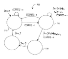
図8は、スレーブ装置600内で実施されるアルゴリズムステートマシン700を示す図である。システムがリセットされると、ステートマシン700は、ライン127がスレーブ600によってトライステートにされる状態710に入る。ライン127のクロックリクエスト信号CLKREQがローである限り、ステートマシン700は状態710のままである。
【0040】
ライン127のクロックリクエスト信号CLKREQがハイになると、ステートマシン700は状態720に入る。状態720の間、ライン127はスレーブ装置600によってトライステートにされ続ける。クロックリクエスト信号CLKREQがハイのままでありかつ周辺バスクロック信号CLKREQが必要でない間はステートマシン700は状態720のままである。
【0041】
ライン127のクロックリクエスト信号CLKREQが再びローになると、ステートマシン700は状態710に戻る。一方、スレーブ600が周辺バスクロック信号CLKを必要とし、ライン127のクロックリクエスト信号がハイであれば、ステートマシン700は状態730に入る。状態730の間、ライン127のクロックリクエスト信号は2クロックサイクルの間スレーブ装置600によってローに引下げられる。その後、ステートマシン700は再び状態710に入り、ライン127はスレーブ装置600によってトライステートにされる。
【0042】
図9は、図2、図5、図7のクロック制御回路120内で実施されるステートマシン800の代替実施例を示す図である。ステートマシン800は、マスタおよびスレーブ装置によってアサートされるクロックリクエスト信号(すなわち、CLKREQ)に応答する。この実施例では、周辺バスクロック信号の再始動および停止は、クロック制御回路120によって直接制御される。なお、電力管理ユニット111は、コンピュータシステムの動作の間普段はクロックジェネレータ122を制御するように構成されてもよい。
【0043】
リセットされると、ステートマシン800は、ライン127のクロックリクエスト信号CLKREQがクロック制御回路120によってトライステートにされ受動的にハイに引上げられ、かつ、周辺バスクロック信号CLKがオンである状態810に入る。ライン127のクロックリクエスト信号が予め定められたクロック数(すなわち、Mクロックサイクル)の間ハイとして検出されれば、ステートマシン800は状態820に入る。
【0044】
状態820の間、ライン127は、クロック制御回路120によってトライステートにされかつハイに引上げられ、周辺バスクロック信号CLKは停止される。なお、クロックジェネレータ122は、周辺バスクロック信号CLKを停止させるようにクロック制御回路120によって電力管理ユニット111を介して直接制御される。ライン127のクロックリクエスト信号CLKREQがたとえば代替バスマスタ108によってローに引下げられるまで、ステートマシン800は状態820のままである。クロックリクエスト信号CLKREQがローにアサートされると、ステートマシン800は状態810に戻り、周辺バスクロック信号CKLが再始動される。
【0045】
その次のクロックサイクルで、クロックリクエスト信号CLKREQがローにアサートされ続ければ、ステートマシン800は状態830に入る。状態830の間、クロック制御回路120は、マスタまたはスレーブ装置が駆動を解放できるようにライン127でのローへの駆動を維持する。同期バスリクエスト信号(すなわち、SREQx)がアサートされれば、バスリクエスト信号がハイにデアサートされるまでステートマシン800は状態830のままである。どのバスリクエスト信号SREQxもローにアサートされずに予め定められたクロックサイクル数(すなわち、Nクロック)が経過すると、ステートマシン800は状態840に入る。状態840の間、ライン127のクロックリクエスト信号CLKREQは1クロックサイクルの間クロック制御回路120によってハイにアサートされる。その後、ステートマシン800は状態810に戻る。
【0046】
ライン127のクロックリクエスト信号が再びローに引下げられそれによってステートマシン800を状態830に入らせるまで、またはMクロックサイクルが経過してステートマシン800が状態820に入り周辺バスクロック信号が停止されるまで、ステートマシン800は状態810のままである。
【0047】
以上のことから、スレーブ装置600は、周辺クロック信号CLKがオンのままであることを要求すれば、クロック制御回路120によるライン127のクロックリクエスト信号(一般に「インジケータ」信号と呼ばれる)のローへのアサーションを検出し(すなわち、図4の状態340の間、または図9の状態840の間)、ステートマシン300の状態330(図4)による、またはステートマシン800の状態830(図9)による決定に応じた付加的な期間クロックを動作させ続けるようにクロックリクエスト信号をローに駆動する。
【0048】
次に図10を参照して、バスインタフェースおよびアービタユニット106の代替的な構成がブロック図で示されている。図を簡略化し明瞭にするために、図5の回路部に対応する回路部には同じ参照番号が付されている。
【0049】
図10のシステムは、クロックリクエスト信号CLKREQを発生することができるバスマスタ(すなわち、マスタ108等)に関して図5を参照して上で記載した説明に従って動作する。このシステムも、クロックリクエスト信号を発生するようには設計されていない従来のバスマスタに適応する。マスタ902は、1つのそのような従来のバスマスタを表わしている。
【0050】
内部でクロックリクエスト信号を発生できない従来の代替バスマスタとの逆方向の互換性を可能にするために、バスマスタ(すなわち、マスタ902)が同期バスリクエスト信号SREQxを確実に発生できるように電力節約モードの間クロック信号のエッジの周期的な発生を制御するプログラマブルクロック制御回路906が設けられる。以下の説明からよりよく理解されるように、電力節約モードの間にクロックエッジが発生される周期速度は、従来のバスマスタの内部構成レジスタから読取られる値に依存する。
【0051】
コンピュータシステム900がリセットされると、マイクロプロセッサ119はBIOSブートコードの実行を開始する。ブーティングの手順の間、マスタ902の構成レジスタ904の内容を読取るために読取動作が実行される。この構成レジスタ904の特定の内容に関して以下に詳細に議論する。
【0052】
BIOSコードはまた、マスタ902がクロックリクエスト信号CLKREQを発生できるかどうかを表わす状態ビットを含む(マスタ902内の)予め定められたレジスタ位置に対して別の読出リクエストを呼出す(なお、クロックリクエスト信号は同様に「クロックラン」信号CLKRUNとも呼ばれ得る)。マスタ902の場合、状態ビットは、マスタ902がクロックリクエスト信号CLKSREQを発生できないことをシステムBIOSに示す。その後、システムBIOSは、マスタ108等の周辺バス102に接続され得る他のいかなるバスマスタ内の類似した状態および構成レジスタをも読取るために付加的な読取リクエストを開始し得る。
【0053】
マスタ902の構成レジスタ904の内容は、マスタが周辺バス102へのアクセスを必要とし得る頻度を表わしている。周辺バス102がPCI規格構成バスである好ましい実施例では、構成レジスタ904は、いわゆるMAXLAT(最大待ち時間)レジスタまたはフィールドとして実施され得る。当業者に容易に認識されるように、MAXLATフィールドは、特定の装置に必要とされるバンド幅、したがってバス調停のためのその優先順位レベルを決定するための他のフィールドとともに用いられる。特定のマスタの待ち時間の値の所望の設定を特定するために、MAXLAT値も用いられる。上で引用したPCI仕様に示されるように、MAXLATフィールドは、特定の装置がPCIバスへのアクセスを必要とする頻度を特定するために用いられる。その値は、1/4μ秒の単位で期間を特定する。値0は、装置が(特定のマスタ内の)待ち時間タイマの設定を特には必要としてないことを表わす。
システムがリセットされると、BIOSブートコードは、周辺バス102に接続される各々の代替バスマスタ内の指定されたMAXLAT構成レジスタを読取り、どのバスマスタがクロックリクエスト信号の発生を支持できるかを判断する。各々のマスタのMAXLATを読取ると、システムは、(クロックリクエスト信号CLKREQを発生できないマスタの中で)周辺バス102へのアクセスを最も頻繁に要求するマスタに対応するMAXLAT値に従ってクロック制御タイマ908を設定する。周辺バス102を最も頻繁に要求するマスタがたとえば2μ秒という最大待ち時間を特定すれば、システムは、1μ秒(すなわち、特定された最大待ち時間の半分)ごとにサイクルを開始する(またはトリガする)ようにクロック制御タイマ908を設定する。その後、電力管理ユニット111が周辺バスクロックを停止させる決定を下すと、クロック制御タイマ908がサイクルを開始する。1μ秒ごとに、クロック制御回路906はクロックジェネレータ122に少なくとも1クロックエッジ(すなわち、ワンショットまたはマルチショット)を与えるようにさせる。これにより、周辺バス102に結合されるマスタ902等のいかなるバスマスタも、そのマスタがクロックリクエスト信号CLKREQを発生できなくても、周辺バス102の統御を得るために同期バスリクエスト信号(すなわち、SREQ2)を確実に発生できる。同期バスリクエスト信号SREQxがリセットされると、プログラマブルクロック制御回路906は、電力管理ユニット111に、周辺バスクロック信号がその最大(または通常)の周波数で駆動される通常動作モードに再び入らせる。それにより、リクエストを出しているマスタがサービスされることが可能となる。
【0054】
なお、好ましい実施例ではクロック制御タイマ908は特定された最大待ち時間の半分の期間で設定されるが、特定された最大待ち時間に比例する(またはそれに依存する)他の値でクロック制御タイマ908を設定してもよい。たとえば、システムに応じて、最大待ち時間の1/3の期間でクロック制御タイマ908を設定することも可能である。しかしながら、最大待ち時間の1/2の期間を設定することにより、各々のマスタがデータを損失することなく周辺バスの統御を確実に得ることができるようにしながら最適な電力の最適化が行なわれると考えられる。
【0055】
したがって、図10のシステムは、周期的なクロックエッジのエッジとエッジとの間でクロック信号をできるだけ長く停止させることにより、電力管理の最適化を適用する。図11は、図10のシステムの動作を示すフロー図である。ステップ950の間、システムBIOSは、スレーブ装置だけが周辺バス102に結合されるかどうかを判断する。もしそうであれば、ステップ952の間に、プログラマブルクロック制御回路はクロックリクエスト信号CLKREQを発生できないバスマスタを適用せずに図5および図7のシステムに従って動作するように設定される。ステップ954による判断に応じて周辺バス102に接続されるマスタの各々がクロックリクエスト信号CLKREQを発生できる場合、同様の動作が設定される。周辺バス102に接続される1つ以上のマスタがクロックリクエスト信号の発生を支持できなれば、ステップ956の間にマスタのMAXLATフィールドが読取られ、ステップ958の間にクロック制御タイマ908はもっとも頻繁にアクセスを要求するマスタ装置によって必要とされる期間の半分の値で設定される。
【0056】
代替的に、電力管理ユニット111が(クロックジェネレータ122を介して)電力節約モードの間(クロック信号を完全に停止させるのではなく)周辺バスクロック信号を低速にする場合、各々のマスタのMAXLATフィールドから読取られる値は、クロック信号が低速にされ得る最小の周波数を決定するために用いられ得る。そのような実施例は図12に示されている。図12の実施例では、クロックジェネレータ122は、最も頻繁に周辺バスを要求するマスタのMAXLATフィールド内で特定される最大待ち時間の値の半分以下の期間で周辺バスクロック信号を発生するようにプログラマブルクロック制御回路906によって設定される。たとえば、マスタ902がレジスタ904の値に従って2μ秒ごとに周辺バス102へのアクセスを必要とし得ることを示し、(クロックリクエスト信号の発生を支持できないマスタのうち)周辺バス102へのアクセスを最も頻繁に要求するのがそのマスタである場合、プログラマブルクロック制御回路906は、電力節約モードの間クロックジェネレータ122に1μ秒(または1μ秒以下)の期間で周辺バスクロック信号を駆動させる周波数制御信号をライン907で発生する。これにより、マスタ902が、少なくとも必要とし得る回数だけ、確実に同期バスリクエスト信号を発生できる。なお、一旦特定のマスタによってバスリクエスト信号SREQxが発生されると、電力管理ユニット111はクロックジェネレータ122に十分な周波数で周辺バスクロック信号を駆動させる。
【0057】
本発明に従ったシステムを用いれば、周辺バスの統御を得るために同期バスリクエスト信号をアサートしなければならない代替バスマスタを適用しながらなおかつ電力管理のために周辺バスクロック信号を停止させるまたは低速にすることができる。
【0058】
周知の種々の回路縮小技術を採用することにより、上述のアルゴリズムステートマシン300、500、700および800を順序論理回路に縮小することが可能である。たとえば、ステートマシン300、500、700および800を順序論理回路に縮小するために、計算機援用設計ツールを用いてもよい。例示的な計算機援用設計ツールには、VHSICハードウェア記述言語、およびVERILOG記述言語が含まれる。
【0059】
図2および図5の電力管理ユニット111は、上述のものの他に種々の付加的な電力管理機能を実現するように構成されてもよい。たとえば、電力管理ユニット111は、1992年11月24日スミス(Smith )他に発行された米国特許番号第5,167,024号に記載される機能と類似した機能を実現するように設計されてもよい。この特許全体を引用によりここに援用する。
【0060】
なお、スレーブ装置600を、種々の特定の周辺装置によって実現することが可能である。たとえば、スレーブ装置600は、ディスクコントローラ装置またはオーディオコントローラ装置であってもよい。
【0061】
さらに、上述の実施例ではクロックジェネレータ122がバスインタフェースおよびアービタユニット106内にあるように示されているが、コンピュータシステム100の種々の代替的な回路ブロックにクロックジェネレータ122を組込むことも可能である。
【0062】
本願は、ゲファート(Gephardt)他による1993年9月22日出願の「周辺バスクロック信号を再始動させ周辺バスの統御を要求するためのシステムおよび方法(System and Method for Re−Starting a Peripheral Bus Clock Signal and Requesting Mastership of a Peripheral Bus 」と題された同一出願人に譲渡された同時係属中の出願連続番号第08/125,406号、およびマクドナルド(MacDonald )による1993年10月1日出願の「スレーブ装置を介して周辺バスクロック信号を制御するためのシステムおよび方法(System and Method For Controlling A Peripheral Bus Clock Signal Through A Slave Device)」と題された同一出願人に譲受された同時係属中の出願連続番号第08/131,092号に関連している。これらの同時係属中の出願を引用によりここに援用する。
【0063】
以上の開示を十分に認識すれば、多数の変形例および変更例が当業者に明らかになるであろう。たとえば、電力節約モードの間クロック信号を完全に停止させる(0Hz)のではなく、周辺バスクロック信号をいかなる周波数レベルにも低減できることを理解されたい。前掲の特許請求の範囲は、そのような変形例および変更例をすべて含むものとして解釈されるものである。
【図面の簡単な説明】
【図1】周辺バスとそれに結合される複数の代替バスマスタとを含むコンピュータシステムのブロック図である。
【図2】周辺バスクロック信号を再始動させるためのクロック制御回路を含むコンピュータシステムの一部分を示すブロック図である。
【図3】1対の信号ドライバをイネーブルするためのフリップフロップを含むコンピュータシステムの一部分を示すブロック図である。
【図4】図2のクロック制御回路内で実施されるアルゴリズムステートマシンを示す図である。
【図5】内部ステートマシンを有し、周辺バスクロック信号をリクエストしかつ同期バスリクエスト信号を発生するための代替バスマスタを含むコンピュータシステムの一部分を示すブロック図である。
【図6】代替バスマスタ内で実施されるアルゴリズムステートマシンを示す図である。
【図7】クロックリクエスト信号をアサートすることができるスレーブ装置を含むコンピュータシステムを示すブロック図である。
【図8】スレーブ装置内で実施されるアルゴリズムステートマシンを示す図である。
【図9】クロック制御回路内で実施されるアルゴリズムステートマシンを示す図である。
【図10】従来のマスタ装置を含むコンピュータシステムを示すブロック図である。
【図11】図10のコンピュータシステム内のプログラマブルクロック制御回路の動作を説明するためのフロー図である。
【図12】従来のマスタ装置を含むコンピュータシステムを示すブロック図である。
【符号の説明】
102 周辺バス
104 ローカルバス
106 バスインタフェースおよびアービタユニット
108 バスマスタ
110 バスマスタ
111 電力管理ユニット
120 クロック制御回路
122 クロックジェネレータ[0001]
FIELD OF THE INVENTION
The present invention relates to power management within a computer system, and more particularly to a system and method for controlling a peripheral bus clock signal.
[0002]
[Description of related technology]
One goal of development being promoted by manufacturers is to reduce the power consumption of computer systems. Reducing power consumption typically reduces heat generation in the system, thereby improving reliability and reducing costs. In addition, reducing power is particularly important in that it maximizes the operating life of portable computer systems powered by batteries.
[0003]
Various techniques have been devised to reduce the power consumption of computer systems. These techniques include improving circuit integration and incorporating improved circuits and power management units (PMUs). Certain power reduction techniques require that the clock signal that drives the inactive circuit portion can be stopped. A system using such a technology typically includes a power management unit that detects or predicts inactive circuit portions and accordingly stops clock signals associated with the inactive circuit portions. By turning off the “unused” clock signal that drives the inactive circuit portion, the overall system power consumption is reduced. A similar technique needs to be able to reduce the frequency of the clock signal that drives the circuit during an operation mode where time is not critical.
[0004]
Although the ability to stop "unused" clock signals has generally been successful in reducing power consumption, this technique is generally used to drive a peripheral bus with an alternate bus master coupled to it. It is not applied to. If you read the following example, you can best understand why this is so.
[0005]
FIG. 1 is a block diagram illustrating a
[0006]
When the
[0007]
In the system of FIG. 1, the peripheral bus clock signal CLK and the synchronous request signal REQx (ie, REQ1 or REQ2) must be asserted by the associated alternate bus master. This requirement is specified by several widely used peripheral bus standards such as the PCI bus standard. Because of these requirements, systems that employ such peripheral bus standards ensure that the peripheral bus clock signal CLK is always on, thereby allowing the alternate bus master to generate a synchronization request signal. Designed. However, in such a system, power is wasted when the peripheral bus is idle.
[0008]
Since slave devices may require a clock signal even after the peripheral bus cycle is over, additional problems arise when employing power reduction techniques in the peripheral bus by stopping the clock (or slowing down the clock). For example, at the end of a peripheral bus cycle, an additional clock cycle may be required for the
[0009]
Yet another problem associated with stopping or slowing the peripheral bus clock signal for power management purposes is that if the peripheral device is unable to restart the peripheral bus clock signal or for a given time If the clock edge is not received within, the external bus master may stop or lose data. Thus, system performance may be degraded or data integrity may be adversely affected. Data integrity is important in any computer system, and traditional peripheral bus masters typically cannot control the associated peripheral bus clock signal, so such conventional bus master devices are for power management. In some cases, the peripheral clock signal may not be compatible with computer systems that are stopped or slowed down. Therefore, backward compatibility between such a computer system and a conventional peripheral device may be limited.
[0010]
SUMMARY OF THE INVENTION
Most of the problems described above are solved by a system and method for controlling a peripheral bus clock signal according to the present invention. The system applies a power saving method that can, for example, stop (or slow down) the peripheral bus clock signal in response to a power management unit. If the alternate bus master requests control of the peripheral bus when the peripheral bus clock signal is stopped, it may be configured to assert a clock request signal for restarting the peripheral bus clock. The clock request signal is sent on the peripheral bus and is therefore received by the clock control circuit. In response, the clock control circuit restarts the peripheral bus clock signal. The alternate bus master can then generate a bus request signal that is synchronous with the peripheral bus clock signal, thereby obtaining a grant signal from the bus arbiter unit.
[0011]
The system can be further configured to provide backward compatibility with a conventional alternative bus master that cannot internally generate bus request signals. In such an embodiment, upon system reset, the BIOS boot code reads a configuration register in each alternate bus master. For PCI-based systems, this configuration register can be a so-called MAXLAT register (or field). The contents of the configuration register represent the frequency with which a particular master can request access to the peripheral bus. As the system reads each master's MAXLAT field, it sets the clock control timer according to the MAXLAT value corresponding to the master that most frequently requests access to the peripheral bus. If the master requesting the peripheral bus most frequently specifies a maximum waiting time of, for example, 2 μs, the system starts a cycle every 1 μs (ie half of the specified maximum waiting time) (or To trigger). Thereafter, if the power management unit decides to stop the peripheral bus clock, the clock control timer begins the cycle. The clock control timer causes the clock generator to provide at least one clock edge (ie, one shot or multi-shot) every 1 microsecond. Thus, any bus master coupled to the peripheral bus can generate a synchronous bus request signal even if it cannot generate a clock request signal, thereby obtaining control of the peripheral bus. In addition, the system applies power management optimization by stopping the clock signal as long as possible between each periodic clock edge. Alternatively, if the power management unit slows down the peripheral bus clock signal during the power saving mode, the value read from each master's MAXLAT field determines the minimum frequency at which the clock signal can be slowed down. Can be used. That is, the clock generator will be set to generate the peripheral bus clock signal in a period of less than half of the maximum latency specified in the master's MAXLAT field that most frequently requests the peripheral bus. With the system according to the present invention, the peripheral bus clock signal is stopped or slowed down for power management while applying an alternative bus master that must assert the synchronous bus request signal to gain control of the peripheral bus. be able to.
[0012]
Other objects and advantages of the present invention will become apparent upon reading the following detailed description with reference to the accompanying drawings.
[0013]
While the invention is susceptible to various modifications and alternative forms, only specific embodiments are shown by way of example in the drawings and will be described in detail below. However, these drawings and detailed description thereof are not intended to limit the invention to the particular forms disclosed, and the invention is intended to be within the spirit and scope of the invention as defined by the appended claims. All variations, equivalents and alternatives are intended to be included.
[0014]
Detailed Description of the Preferred Embodiment
Referring now to FIG. 2, a portion of a
[0015]
[0016]
[0017]
The
[0018]
The bus interface and
[0019]
The bus interface and
[0020]
Next, the operation of the
[0021]
When one of the
[0022]
At the rising edge of the first peripheral clock signal CLK, the logic low signal on line 128 (ie, signal AREQ 1) is latched into flip-flop 112 and driven by the output of flip-flop 112. Therefore, the synchronization request signal SREQ1, which depends on the output state of the flip-flop 112, goes low. Note that the low transition of the signal SREQ1 occurs synchronously with the clock signal CLK.
[0023]
When the bus interface and
[0024]
In the preferred embodiment, when control of
[0025]
Note that in the preferred embodiment, signal
[0026]
Referring again to FIG. 2, if asynchronous request signals AREQ1 and AREQ2 are asserted simultaneously or simultaneously, indicating that both
[0027]
Next, consider the internal logic of the
[0028]
[0029]
The
[0030]
[0031]
The
[0032]
Referring again to FIG. 2, note that flip-
[0033]
In another embodiment as shown in FIG. 5, a state machine is incorporated into each alternate bus master to generate a clock request signal CLKREQ and a synchronization request signal SREQx. Circuit parts corresponding to those in FIG. 2 are given the same reference numerals. FIG. 6 is a diagram illustrating an
[0034]
Referring to FIG. 6 together with FIGS. 4 and 5, after reset, the
[0035]
With the systems shown in FIGS. 2 and 5, the peripheral bus clock signal can be stopped for power management while applying an alternative bus master that must assert the synchronous bus signal to gain control of the peripheral bus. it can. Therefore, the power consumption of the computer system can be reduced while maintaining wide compatibility.
[0036]
Referring now to FIG. 7, a portion of a similar computer system in which
[0037]
[0038]
During operation of the embodiment of FIG. 7,
[0039]
FIG. 8 is a diagram showing an
[0040]
[0041]
When the clock request signal CLKREQ on
[0042]
FIG. 9 is a diagram illustrating an alternative embodiment of
[0043]
When reset,
[0044]
During
[0045]
In the next clock cycle,
[0046]
Until the clock request signal on
[0047]
From the above, if the
[0048]
Referring now to FIG. 10, an alternative configuration for the bus interface and
[0049]
The system of FIG. 10 operates in accordance with the description described above with reference to FIG. 5 for a bus master (ie,
[0050]
In order to allow backward compatibility with a conventional alternative bus master that cannot internally generate a clock request signal, the power saving mode can be used to ensure that the bus master (ie, master 902) can generate the synchronous bus request signal SREQx. A programmable
[0051]
When the
[0052]
The BIOS code also includes a status bit that indicates whether the
[0053]
The contents of
When the system is reset, the BIOS boot code reads the designated MAXLAT configuration register in each alternate bus master connected to
[0054]
Note that in the preferred embodiment, the clock control timer 908 is set at half the specified maximum latency, but with other values proportional to (or dependent on) the specified maximum latency. May be set. For example, the clock control timer 908 can be set in a period of 1/3 of the maximum waiting time depending on the system. However, by setting a period of 1/2 of the maximum waiting time, optimal power optimization is performed while each master can reliably obtain control of the peripheral bus without losing data. it is conceivable that.
[0055]
Thus, the system of FIG. 10 applies power management optimization by stopping the clock signal as long as possible between the edges of the periodic clock edges. FIG. 11 is a flowchart showing the operation of the system of FIG. During
[0056]
Alternatively, if the
[0057]
With the system according to the present invention, the peripheral bus clock signal is stopped or slowed down for power management while applying an alternative bus master that must assert the synchronous bus request signal to gain control of the peripheral bus. can do.
[0058]
By employing various well-known circuit reduction techniques, it is possible to reduce the
[0059]
The
[0060]
Note that the
[0061]
Further, although the
[0062]
This application is filed on Sep. 22, 1993 by “Gerhardt et al.,“ System and Method for Re-Starting a Peripheral Bus Clock ”to restart the peripheral bus clock signal and request control of the peripheral bus. Copending application serial number 08 / 125,406 assigned to the same applicant entitled "Signal and Requesting Mastership of a Peripheral Bus", and MacDonald's " System and method for controlling a peripheral for controlling a peripheral bus clock signal via a slave device related to co-pending application serial number 08 / 131,092, assigned to the same applicant entitled "Al Bus Clock Through A Slave Device". Cite these co-pending applications. Is incorporated herein by reference.
[0063]
Numerous variations and modifications will become apparent to those skilled in the art once the above disclosure is fully appreciated. For example, it should be understood that the peripheral bus clock signal can be reduced to any frequency level, rather than completely stopping the clock signal (0 Hz) during the power saving mode. The following claims are to be construed as including all such variations and modifications.
[Brief description of the drawings]
FIG. 1 is a block diagram of a computer system including a peripheral bus and a plurality of alternative bus masters coupled thereto.
FIG. 2 is a block diagram illustrating a portion of a computer system including a clock control circuit for restarting a peripheral bus clock signal.
FIG. 3 is a block diagram illustrating a portion of a computer system that includes a flip-flop for enabling a pair of signal drivers.
FIG. 4 is a diagram showing an algorithm state machine implemented in the clock control circuit of FIG. 2;
FIG. 5 is a block diagram illustrating a portion of a computer system having an internal state machine and including an alternative bus master for requesting a peripheral bus clock signal and generating a synchronous bus request signal.
FIG. 6 shows an algorithm state machine implemented in an alternative bus master.
FIG. 7 is a block diagram illustrating a computer system including a slave device that can assert a clock request signal.
FIG. 8 shows an algorithm state machine implemented within a slave device.
FIG. 9 shows an algorithm state machine implemented in the clock control circuit.
FIG. 10 is a block diagram showing a computer system including a conventional master device.
FIG. 11 is a flowchart for explaining the operation of the programmable clock control circuit in the computer system of FIG. 10;
FIG. 12 is a block diagram showing a computer system including a conventional master device.
[Explanation of symbols]
102 Peripheral bus
104 Local bus
106 Bus interface and arbiter unit
108 Bus master
110 Bus master
111 Power management unit
120 clock control circuit
122 clock generator
Claims (7)
マイクロプロセッサと、
前記マイクロプロセッサに結合されるローカルバスと、
周辺バスと、
前記ローカルバスと前記周辺バスとに結合され、前記ローカルバスと前記周辺バスとの間でのデータおよびアドレス信号の転送を制御しかつ前記周辺バスの統御を調停するように構成されるバスインタフェースおよびアービタユニットと、
前記周辺バス上に周辺バスクロック信号を与えるように結合されたクロックジェネレータ回路とを含み、前記周辺バスクロック信号は選択的に制御されるように構成され、前記コンピュータシステムは、
前記周辺バスに或るアクセス速度でアクセスを求める代替バスマスタをさらに含み、前記代替バスマスタは前記周辺バスに結合され、前記コンピュータシステムはさらに、
前記代替バスマスタと前記クロックジェネレータ回路とに結合され、通常モードの間第1の予め定められた速度で前記周辺バスクロック信号を駆動するように構成される、クロック制御回路を含み、
前記クロック制御回路は、さらに電力低減モードの間第2の予め定められた速度で少なくとも1つのクロックエッジを与えるように構成され、前記第2の予め定められた速度は前記第1の予め定められた速度より低く、前記第2の予め定められた速度は前記代替バスマスタの前記アクセス速度に基づき、前記クロック制御回路は、前記代替バスマスタ内の記憶場所から前記代替バスマスタのアクセス速度を指示する値を読出すように構成される、コンピュータシステム。A computer system,
A microprocessor;
A local bus coupled to the microprocessor;
With peripheral buses,
A bus interface coupled to the local bus and the peripheral bus, configured to control transfer of data and address signals between the local bus and the peripheral bus and to arbitrate control of the peripheral bus; and Arbiter unit,
A clock generator circuit coupled to provide a peripheral bus clock signal on the peripheral bus, wherein the peripheral bus clock signal is configured to be selectively controlled, the computer system comprising:
And further comprising an alternative bus master seeking access to the peripheral bus at a certain access speed, the alternative bus master being coupled to the peripheral bus, and the computer system further comprising:
A clock control circuit coupled to the alternative bus master and the clock generator circuit and configured to drive the peripheral bus clock signal at a first predetermined speed during a normal mode ;
The clock control circuit is further configured to provide at least one clock edge at a second predetermined speed during the power reduction mode, the second predetermined speed being the first predetermined speed. The second predetermined speed is based on the access speed of the alternative bus master , and the clock control circuit sets a value indicating the access speed of the alternative bus master from a storage location in the alternative bus master. A computer system configured to read .
マイクロプロセッサと、
前記マイクロプロセッサに結合されたローカルバスと、
周辺バスと、
前記ローカルバスと前記周辺バスとに結合され、前記ローカルバスと前記周辺バスとの間でのデータおよびアドレス信号の転送を制御しかつ前記周辺バスの統御を調停するように構成されるバスインタフェースおよびアービタユニットと、
前記周辺バス上に周辺バスクロック信号を与えるように結合されたクロックジェネレータ回路とを含み、前記周辺バスクロック信号は選択的に制御されるように構成され、前記コンピュータシステムは、
前記周辺バスに結合された代替バスマスタを含み、さらに、前記コンピュータシステムは、
前記代替バスマスタと前記クロックジェネレータ回路とに結合されるクロック制御回路を含み、前記クロック制御回路は、通常モードの間第1の予め定められた速度で前記周辺バスクロック信号を駆動し、電力低減モードの間第2の予め定められた速度で前記周辺バスクロック信号を駆動するように構成され、前記第2の予め定められた速度は前記第1の予め定められた速度より低く、
前記クロック制御回路は前記電力低減モードの間に前記第2の予め定められた速度で少なくとも1つのクロックエッジを与えるように構成され、前記第2の予め定められた速度は前記代替バスマスタが前記周辺バスにアクセスを求める、最大待ち時間に基づき、前記クロック制御回路は、前記代替バスマスタ内の記憶場所から前記代替バスマスタのアクセス速度を指示する値を読出すように構成される、コンピュータシステム。A computer system,
A microprocessor;
A local bus coupled to the microprocessor;
With peripheral buses,
A bus interface coupled to the local bus and the peripheral bus, configured to control transfer of data and address signals between the local bus and the peripheral bus and to arbitrate control of the peripheral bus; and Arbiter unit,
A clock generator circuit coupled to provide a peripheral bus clock signal on the peripheral bus, wherein the peripheral bus clock signal is configured to be selectively controlled, the computer system comprising:
An alternative bus master coupled to the peripheral bus , and the computer system further comprising:
Includes a clock control circuit and the alternate bus master Ru coupled to said clock generator circuit, the clock control circuit, said driving peripheral bus clock signal, power reduction in a first predetermined speed during the normal mode Configured to drive the peripheral bus clock signal at a second predetermined speed during a mode, wherein the second predetermined speed is lower than the first predetermined speed;
It said clock control circuit is configured to provide at least one clock edge in said second predetermined rate during said power reduction mode, said second predetermined speed is the alternate bus master the peripheral A computer system, wherein the clock control circuit is configured to read a value indicating an access speed of the alternative bus master from a storage location in the alternative bus master based on a maximum waiting time seeking access to the bus.
マイクロプロセッサと、
前記マイクロプロセッサに結合されたローカルバスと、
周辺バスと、
前記ローカルバスと前記周辺バスとに結合され、前記ローカルバスと前記周辺バスとの間でのデータおよびアドレス信号の転送を制御するための手段とを含み、前記制御手段は前記周辺バスの統御を調停するための手段を含み、前記コンピュータシステムは、
前記周辺バス上に周辺バスクロック信号を選択的に発生させるための手段を含み、前記選択的に発生させる手段は前記周辺バスクロック信号のクロック速度を選択するための手段を含み、前記クロック速度は、通常モードに対応する第1のクロック速度と、動作の電力低減モードに対応する第2のクロック速度を含み、前記第2のクロック速度は前記第1のクロック速度より低く、前記コンピュータシステムは、
前記周辺バスに結合されたバスマスタを含み、前記バスマスタは前記周辺バスにアクセスを要求するのにクロック信号を必要とし、前記コンピュータシステムはさらに、
前記電力低減モードの間に前記バスマスタがバスアクセスを要求できるように前記周辺バス上に前記第2のクロック速度を与えるための手段を含み、前記第2のクロック速度は、前記バスマスタのアクセス速度に基づき、前記バスマスタは、前記バスマスタのアクセス速度を指示する値を保持する記憶場所を含む、コンピュータシステム。A computer system,
A microprocessor;
A local bus coupled to the microprocessor;
With peripheral buses,
Means for controlling the transfer of data and address signals between the local bus and the peripheral bus, and the control means controls the peripheral bus. Means for arbitrating, said computer system comprising:
Means for selectively generating a peripheral bus clock signal on said peripheral bus, said means for selectively generating includes means for selecting a clock speed of said peripheral bus clock signal, said clock speed being A first clock speed corresponding to a normal mode and a second clock speed corresponding to a power reduction mode of operation, wherein the second clock speed is lower than the first clock speed, and the computer system includes:
A bus master coupled to the peripheral bus, the bus master requiring a clock signal to request access to the peripheral bus, and the computer system further comprises:
Means for providing the second clock speed on the peripheral bus so that the bus master can request bus access during the power reduction mode, the second clock speed being equal to the access speed of the bus master. Based on the computer system , the bus master includes a storage location holding a value indicating the access speed of the bus master .
Applications Claiming Priority (2)
| Application Number | Priority Date | Filing Date | Title |
|---|---|---|---|
| US23481994A | 1994-04-28 | 1994-04-28 | |
| US234819 | 1994-04-28 |
Publications (2)
| Publication Number | Publication Date |
|---|---|
| JPH07302132A JPH07302132A (en) | 1995-11-14 |
| JP3633998B2 true JP3633998B2 (en) | 2005-03-30 |
Family
ID=22882960
Family Applications (1)
| Application Number | Title | Priority Date | Filing Date |
|---|---|---|---|
| JP10408695A Expired - Lifetime JP3633998B2 (en) | 1994-04-28 | 1995-04-27 | Computer system |
Country Status (5)
| Country | Link |
|---|---|
| US (1) | US5628019A (en) |
| EP (1) | EP0679982B1 (en) |
| JP (1) | JP3633998B2 (en) |
| AT (1) | ATE231254T1 (en) |
| DE (1) | DE69529362T2 (en) |
Families Citing this family (27)
| Publication number | Priority date | Publication date | Assignee | Title |
|---|---|---|---|---|
| US5678065A (en) * | 1994-09-19 | 1997-10-14 | Advanced Micro Devices, Inc. | Computer system employing an enable line for selectively adjusting a peripheral bus clock frequency |
| ATE205616T1 (en) * | 1994-10-19 | 2001-09-15 | Advanced Micro Devices Inc | INTEGRATED PROCESSOR SYSTEMS FOR PORTABLE INFORMATION DEVICES |
| US5805923A (en) * | 1995-05-26 | 1998-09-08 | Sony Corporation | Configurable power management system having a clock stabilization filter that can be enabled or bypassed depending upon whether a crystal or can oscillator is used |
| JP2974950B2 (en) * | 1995-10-26 | 1999-11-10 | インターナショナル・ビジネス・マシーンズ・コーポレイション | Information processing system |
| US5907688A (en) * | 1996-06-28 | 1999-05-25 | Intel Corporation | Smart arbitration for non-symmetric data streams |
| US6079022A (en) * | 1996-10-11 | 2000-06-20 | Intel Corporation | Method and apparatus for dynamically adjusting the clock speed of a bus depending on bus activity |
| JP3592547B2 (en) * | 1998-09-04 | 2004-11-24 | 株式会社ルネサステクノロジ | Information processing apparatus and signal transfer method |
| US6763478B1 (en) * | 2000-10-24 | 2004-07-13 | Dell Products, L.P. | Variable clock cycle for processor, bus and components for power management in an information handling system |
| US6694441B1 (en) * | 2000-11-15 | 2004-02-17 | Koninklijke Philips Electronics N.V. | Power management method and arrangement for bus-coupled circuit blocks |
| KR100710942B1 (en) * | 2001-04-25 | 2007-04-24 | 엘지전자 주식회사 | Apparatus for controlling a device clock on connected peripheral component interconnect bus |
| JP4733877B2 (en) * | 2001-08-15 | 2011-07-27 | 富士通セミコンダクター株式会社 | Semiconductor device |
| JP3447725B2 (en) * | 2001-10-23 | 2003-09-16 | 沖電気工業株式会社 | Competitive mediation device |
| TW533357B (en) * | 2001-12-14 | 2003-05-21 | Via Tech Inc | Method of hot switching the data transmission rate of bus |
| JP3835328B2 (en) | 2002-03-27 | 2006-10-18 | ブラザー工業株式会社 | Memory control device |
| US7281148B2 (en) * | 2004-03-26 | 2007-10-09 | Intel Corporation | Power managed busses and arbitration |
| US7606960B2 (en) * | 2004-03-26 | 2009-10-20 | Intel Corporation | Apparatus for adjusting a clock frequency of a variable speed bus |
| KR100630693B1 (en) * | 2004-07-28 | 2006-10-02 | 삼성전자주식회사 | Bus arbitration system and method improving power consumption |
| WO2006131142A1 (en) * | 2005-06-10 | 2006-12-14 | Freescale Semiconductor, Inc. | Method and device for frame synchronization |
| WO2006131143A1 (en) * | 2005-06-10 | 2006-12-14 | Freescale Semiconductor, Inc. | Device and method for media access control |
| JP2007058279A (en) * | 2005-08-22 | 2007-03-08 | Oki Electric Ind Co Ltd | Power-down shifting system |
| JP4917649B2 (en) * | 2006-10-31 | 2012-04-18 | フリースケール セミコンダクター インコーポレイテッド | Network and method for setting a time reference for nodes in the network |
| JP5277533B2 (en) * | 2006-11-15 | 2013-08-28 | ヤマハ株式会社 | Digital signal processor |
| CN101329589B (en) * | 2008-07-28 | 2011-04-27 | 北京中星微电子有限公司 | Control system and method of low power consumption read-write register |
| US10817043B2 (en) * | 2011-07-26 | 2020-10-27 | Nvidia Corporation | System and method for entering and exiting sleep mode in a graphics subsystem |
| US10503674B2 (en) | 2016-02-03 | 2019-12-10 | Samsung Electronics Co., Ltd. | Semiconductor device including a clock source for generating a clock signal and a clock control circuit for controlling the clock source in hardware, a semiconductor system including the semiconductor device, and a method of operating the semiconductor device |
| JP6906369B2 (en) * | 2017-05-29 | 2021-07-21 | キヤノン株式会社 | Computer systems, their control methods, and programs |
| US11144358B1 (en) | 2018-12-06 | 2021-10-12 | Pure Storage, Inc. | Asynchronous arbitration of shared resources |
Family Cites Families (14)
| Publication number | Priority date | Publication date | Assignee | Title |
|---|---|---|---|---|
| US4381552A (en) * | 1978-12-08 | 1983-04-26 | Motorola Inc. | Stanby mode controller utilizing microprocessor |
| US4748559A (en) * | 1979-08-09 | 1988-05-31 | Motorola, Inc. | Apparatus for reducing power consumed by a static microprocessor |
| JPS58127262A (en) * | 1982-01-25 | 1983-07-29 | Toshiba Corp | Microcomputer |
| JPS59200327A (en) * | 1983-04-26 | 1984-11-13 | Nec Corp | Control system of peripheral device |
| JPS61156338A (en) * | 1984-12-27 | 1986-07-16 | Toshiba Corp | Multiprocessor system |
| US5150467A (en) * | 1987-09-04 | 1992-09-22 | Digital Equipment Corporation | Method and apparatus for suspending and restarting a bus cycle |
| DE68925615T2 (en) * | 1988-11-10 | 1996-09-12 | Motorola Inc | Digital computer system with low power consumption mode |
| US5167024A (en) * | 1989-09-08 | 1992-11-24 | Apple Computer, Inc. | Power management for a laptop computer with slow and sleep modes |
| US5263172A (en) * | 1990-04-16 | 1993-11-16 | International Business Machines Corporation | Multiple speed synchronous bus having single clock path for providing first or second clock speed based upon speed indication signals |
| US5341508A (en) * | 1991-10-04 | 1994-08-23 | Bull Hn Information Systems Inc. | Processing unit having multiple synchronous bus for sharing access and regulating system bus access to synchronous bus |
| US5392422A (en) * | 1992-06-26 | 1995-02-21 | Sun Microsystems, Inc. | Source synchronized metastable free bus |
| US5339395A (en) * | 1992-09-17 | 1994-08-16 | Delco Electronics Corporation | Interface circuit for interfacing a peripheral device with a microprocessor operating in either a synchronous or an asynchronous mode |
| US5392437A (en) * | 1992-11-06 | 1995-02-21 | Intel Corporation | Method and apparatus for independently stopping and restarting functional units |
| US5396602A (en) * | 1993-05-28 | 1995-03-07 | International Business Machines Corp. | Arbitration logic for multiple bus computer system |
-
1995
- 1995-03-02 AT AT95301340T patent/ATE231254T1/en not_active IP Right Cessation
- 1995-03-02 DE DE69529362T patent/DE69529362T2/en not_active Expired - Lifetime
- 1995-03-02 EP EP95301340A patent/EP0679982B1/en not_active Expired - Lifetime
- 1995-04-27 JP JP10408695A patent/JP3633998B2/en not_active Expired - Lifetime
-
1996
- 1996-06-04 US US08/656,840 patent/US5628019A/en not_active Expired - Lifetime
Also Published As
| Publication number | Publication date |
|---|---|
| ATE231254T1 (en) | 2003-02-15 |
| EP0679982B1 (en) | 2003-01-15 |
| JPH07302132A (en) | 1995-11-14 |
| US5628019A (en) | 1997-05-06 |
| DE69529362D1 (en) | 2003-02-20 |
| EP0679982A1 (en) | 1995-11-02 |
| DE69529362T2 (en) | 2003-10-30 |
Similar Documents
| Publication | Publication Date | Title |
|---|---|---|
| JP3633998B2 (en) | Computer system | |
| US5600839A (en) | System and method for controlling assertion of a peripheral bus clock signal through a slave device | |
| US5625807A (en) | System and method for enabling and disabling a clock run function to control a peripheral bus clock signal | |
| US7188262B2 (en) | Bus arbitration in low power system | |
| US6163848A (en) | System and method for re-starting a peripheral bus clock signal and requesting mastership of a peripheral bus | |
| US7155618B2 (en) | Low power system and method for a data processing system | |
| US5590341A (en) | Method and apparatus for reducing power consumption in a computer system using ready delay | |
| US6173348B1 (en) | Using a control line to insert a control message during a data transfer on a bus | |
| US6148357A (en) | Integrated CPU and memory controller utilizing a communication link having isochronous and asynchronous priority modes | |
| US20070038829A1 (en) | Wait aware memory arbiter | |
| JP5102789B2 (en) | Semiconductor device and data processor | |
| US7155631B2 (en) | Information processing unit with a clock control circuit having access to the system bus during system clock changes | |
| JP3568592B2 (en) | Computer system and method for controlling peripheral bus clock signals | |
| US6199132B1 (en) | Communication link with isochronous and asynchronous priority modes | |
| JPH1153049A (en) | Computer system | |
| EP2109029B1 (en) | Apparatus and method for address bus power control | |
| JP4182246B2 (en) | Bus sharing system and bus sharing method | |
| US6618790B1 (en) | Burst suspend and resume with computer memory | |
| JPH10320349A (en) | Processor and data transfer system using the processor | |
| US6016551A (en) | Method and apparatus for masking and unmasking a clock signal in an integrated circuit | |
| JPS6054065A (en) | Synchronous controller | |
| JP3713488B2 (en) | Computer system and operation control method thereof | |
| JPH11328111A (en) | Clock synchronous type bus circuit |
Legal Events
| Date | Code | Title | Description |
|---|---|---|---|
| A02 | Decision of refusal |
Free format text: JAPANESE INTERMEDIATE CODE: A02 Effective date: 20040316 |
|
| A521 | Request for written amendment filed |
Free format text: JAPANESE INTERMEDIATE CODE: A523 Effective date: 20040708 |
|
| A911 | Transfer to examiner for re-examination before appeal (zenchi) |
Free format text: JAPANESE INTERMEDIATE CODE: A911 Effective date: 20040722 |
|
| TRDD | Decision of grant or rejection written | ||
| A01 | Written decision to grant a patent or to grant a registration (utility model) |
Free format text: JAPANESE INTERMEDIATE CODE: A01 Effective date: 20041214 |
|
| A61 | First payment of annual fees (during grant procedure) |
Free format text: JAPANESE INTERMEDIATE CODE: A61 Effective date: 20041222 |
|
| R150 | Certificate of patent or registration of utility model |
Free format text: JAPANESE INTERMEDIATE CODE: R150 |
|
| FPAY | Renewal fee payment (event date is renewal date of database) |
Free format text: PAYMENT UNTIL: 20090107 Year of fee payment: 4 |
|
| FPAY | Renewal fee payment (event date is renewal date of database) |
Free format text: PAYMENT UNTIL: 20100107 Year of fee payment: 5 |
|
| FPAY | Renewal fee payment (event date is renewal date of database) |
Free format text: PAYMENT UNTIL: 20110107 Year of fee payment: 6 |
|
| FPAY | Renewal fee payment (event date is renewal date of database) |
Free format text: PAYMENT UNTIL: 20110107 Year of fee payment: 6 |
|
| FPAY | Renewal fee payment (event date is renewal date of database) |
Free format text: PAYMENT UNTIL: 20120107 Year of fee payment: 7 |
|
| FPAY | Renewal fee payment (event date is renewal date of database) |
Free format text: PAYMENT UNTIL: 20130107 Year of fee payment: 8 |
|
| R250 | Receipt of annual fees |
Free format text: JAPANESE INTERMEDIATE CODE: R250 |
|
| R250 | Receipt of annual fees |
Free format text: JAPANESE INTERMEDIATE CODE: R250 |
|
| EXPY | Cancellation because of completion of term |