EP1283565A2 - Verbinder ohne Lichtbogen - Google Patents
Verbinder ohne Lichtbogen Download PDFInfo
- Publication number
- EP1283565A2 EP1283565A2 EP02255391A EP02255391A EP1283565A2 EP 1283565 A2 EP1283565 A2 EP 1283565A2 EP 02255391 A EP02255391 A EP 02255391A EP 02255391 A EP02255391 A EP 02255391A EP 1283565 A2 EP1283565 A2 EP 1283565A2
- Authority
- EP
- European Patent Office
- Prior art keywords
- contact
- electrical connector
- terminal
- mating
- auxiliary
- Prior art date
- Legal status (The legal status is an assumption and is not a legal conclusion. Google has not performed a legal analysis and makes no representation as to the accuracy of the status listed.)
- Granted
Links
Images


Classifications
-
- H—ELECTRICITY
- H01—ELECTRIC ELEMENTS
- H01R—ELECTRICALLY-CONDUCTIVE CONNECTIONS; STRUCTURAL ASSOCIATIONS OF A PLURALITY OF MUTUALLY-INSULATED ELECTRICAL CONNECTING ELEMENTS; COUPLING DEVICES; CURRENT COLLECTORS
- H01R13/00—Details of coupling devices of the kinds covered by groups H01R12/70 or H01R24/00 - H01R33/00
- H01R13/46—Bases; Cases
- H01R13/53—Bases or cases for heavy duty; Bases or cases for high voltage with means for preventing corona or arcing
-
- H—ELECTRICITY
- H01—ELECTRIC ELEMENTS
- H01R—ELECTRICALLY-CONDUCTIVE CONNECTIONS; STRUCTURAL ASSOCIATIONS OF A PLURALITY OF MUTUALLY-INSULATED ELECTRICAL CONNECTING ELEMENTS; COUPLING DEVICES; CURRENT COLLECTORS
- H01R13/00—Details of coupling devices of the kinds covered by groups H01R12/70 or H01R24/00 - H01R33/00
- H01R13/66—Structural association with built-in electrical component
- H01R13/6608—Structural association with built-in electrical component with built-in single component
- H01R13/6616—Structural association with built-in electrical component with built-in single component with resistor
Definitions
- This invention relates to an electrical connector including means for preventing or suppressing an arc when power contacts are disconnected or separated while they carry substantial power or electrical current.
- This invention also relates to an electrical connector that preferentially uses a positive temperature coefficient resistor shunted between contacts that are disconnected sequentially so that voltage and current will be below a threshold at which arcing might occur, when each contact is separated from a mating contact.
- the amount of arc damage experienced by the contacts depends on their physical structure, the load current, the supply voltage, the speed of separation, the characteristics of the load (resistive, capacitive, inductive) as well as other factors.
- PTC Positive Temperature Coefficient Resistance
- resistorsor switches have been used, or suggested for use, in circuit breakers that are used to break fault currents, specifically defined and excessive overcurrents, for which these circuit breakers are rated.
- electrical connectors are expected to carry a wide range of currents during actual use. Even though an electrical connector may be rated to carry a specific current, in actual practice, an electrical connector will carry currents over a large range due to variations in the load. The cost, size and weight of an electrical connector will generally increase with increasing current rating, so the lowest rated connector suitable for use in a specific application will normally be used.
- the trip time varies for a PTC device in which resistance is dependent upon the temperature of the device, and the temperature is dependant upon current because of I 2 R heating.
- the trip time for a PTC device used in an electrical connector will vary because of the wide range of currents that will be carried by a particular electrical connector.
- both halves of electrical contacts remain within the same physical device.
- the contacts separate from each other, but only by a well defined and fixed distance, and the separated contacts are still part of the device package.
- the essential function of electrical connectors is to totally separate the two contact halves. No physical connection remains between the two halves, and all physical ties are broken between two mating connector contacts.
- the PTC device In order to protect separating electrical contacts that are carrying arc-producing power, the PTC device must be connected across the contact pair until the current is sufficiently reduced to prevent arcing.
- the problem is that a physical electrical connection to both halves of the separating electrical contact must be maintained in a conventional use of a PTC device yet, in a connector, all physical connections must be broken.
- the instant invention preferably employs a positive temperature coefficient (PTC) resistor in an electrical connector in series with an auxiliary electrical contact portion or contact terminal, the combination of which is in parallel with a main electrical contact portion or contact terminal, which disconnects first.
- PTC positive temperature coefficient
- Both the main and the auxiliary contacts are matable with a terminal or terminals in a mating electrical connector.
- the main and auxiliary contacts are male terminals or blades that mate with a female or receptacle terminal in the mating electrical connector.
- the PTC resistive member could also be employed with the female terminals.
- the PTC resistive member should, however, only be employed with the terminals in one half of a mating pair of electrical connectors.
- the main or auxiliary contact portions or terminals in one of the two connectors must incorporate the PTC member.
- a conventional discrete PTC member such as a commercially available POLYSWITCH® device
- the main and auxiliary contact portions or terminals in the other of the two mating connectors must be connected together directly, with no discrete PTC device between them.
- the PTC means may be located in both connectors.
- a discrete PTC resistive member can be employed into the main and auxiliary contact terminals so that the PTC device can form an integrated unit.
- One means for forming such an integrated unit would be to mold a PTC conductive polymer between the main and auxiliary contact terminals.
- the PTC conductive polymer could also be overmolded around portions of the main and auxiliary contact terminals, with the PTC conductive polymer being molded between the main and auxiliary contact terminals. Insert molding techniques could be used to position the PTC conductive polymer between, the main and auxiliary contact terminals.
- the PTC conductive polymer could also be a discrete component that is molded as a shape that would conform to parts of the main and auxiliary contact terminals and this discrete component could be bonded between the main and auxiliary contact terminals using solder, a conductive adhesive or some other conductive bonding agent.
- the PTC member comprises a conductive polymer member in which conductive particles are contained within a polymer matrix. Normally the conductive particles form a conductive path that have a resistance that is larger than the resistance of the main terminal so that under normal mated operation, the main contact would carry substantially all of the current. However, as current increases in the PTC member, the polymer expands and the resistance increases. When current through the PTC member increases rapidly due to disconnection of the main contact terminal, the resistance will increase rapidly due to I 2 R heating of the polymer.
- the disconnect time for the main contact must be less than the time for the resistance of the PTC member to increase too greatly. Most of the current through the main contact must be carried by the PTC member and the auxiliary contact until the main contact has moved to a position in which arcing is no longer possible. Before the auxiliary contact is disconnected from the mating terminal, the resistance in the PTC member must increase so that the current flow through the auxiliary contact will drop below the arcing threshold before the auxiliary contact is unmated. This time is called the trip time of this PTC resitive member.
- the electrical connector of this invention employs latches that cannot be activated, after the disconnection of the main contact, for a time interval that will be greater than the maximum trip time for the PTC member.
- latches must also permit rapid movement between the two electrical connectors as the main contact moves through a portion of its path in which it is susceptible to arcing.
- the auxiliary contact must move rapidly through an arc susceptible region as it is disconnected.
- the preferred embodiments of this invention therefore use multiple sets of latches that must be sequentially disengaged, and which provide a time delay between disconnection of a first set of latches and the disconnection of a second set of latches. This time delay should be longer than the maximum PTC trip time.
- This multiple latch configuration provides a versatile implementation of the invention. If, however, a specific electrical connector serves loads with a small difference between maximum and minimum current loads, a simpler latch mechanism can be utilized. The maximum achievable parting velocity and the added length of the auxiliary contact could in some cases provide adequate time for the PTC device to trip.
- This true arc consists of several sub-parts including the cathode spot, the cathode drop region, an extremely hot plasma channel, the anode drop region and the anode spot.
- the plasma channel is about 5000° C and the anode and cathode spots reach about 2000° C at 10-20 ampere currents.
- PTC Positive Temperature Coefficient
- the leads on a discrete device could also be attached by contact springs or by crimps or by latching detents on the contacts.
- a conductive polymer, of the type exemplified by this discrete device can also be overmolded onto contact terminals to form a new component, or a PTC device can be integrated with the contact terminals to form an integrated component or unit.
- This approach may not eliminate the relatively benign spark that may occur when a high-energy circuit is connected. In the energy range of interest, this benign spark tends to do little damage to the contact base metal and to the shape of the contact.
- the general characteristics of POLYSWITCH® devices are discussed in US Patent 5,737,160 and the patents incorporated by reference therein.
- Figure 1 shows the concept for an arc-less power contact in accordance with the instant invention.
- Representative male and female, or blade 7 and receptacle 9 terminals, according to this invention, are shown in various stages of disconnection or unmating.
- the main contact 1 or the main portion of the contact, carries the load current during normal operation.
- the main contact is shunted by a series connected, longer auxiliary contact 3 or contact portion and by a positive temperature coefficient resistance 5 or resistor, located between the main contact and the auxiliary contact.
- FIG. 1 illustrates the four stages that occur during separation of the plug connector from the mating receptacle connector.
- stage 0 Fig 1a: main contact mated; auxiliary contact mated; and PTC reset
- the contact is carrying a high current.
- the current is primarily flowing through the main contact or the main portion of the contact. Only a relatively small shunt current flows through the series connected positive temperature coefficient resistance or resistor (PTC) and the auxiliary portion of the contact.
- PTC positive temperature coefficient resistance or resistor
- Stage 0 represents the normal operating configuration of a connector assembly. Relative movement of the two contacts in this position would result in the normal wiping action between two contact surfaces.
- Stage 1 (Fig. 1b: main contact open; auxiliary contact mated; and PTC on) shows the configuration in which the main contact or main contact portion has been separated or disconnected from the mating contact in the other connector.
- the main blade is separated from the main receptacle through the main contact disconnect zone (MDZ), which occurs between Stage 0 and Stage 1, in which the main blade contact is in the process of unmating from the corresponding female or receptacle contact. While the two contacts are in this main disconnect zone, the two contacts are not completely separated. Contact bounce may occur as the spring members flex and as irregular surfaces on the contact result in momentary separation and engagement.
- MDZ main contact disconnect zone
- the main contact When the mating contacts have moved to the position identified as Stage 1, the main contact is physically separated from its mating contact so that arcing can no longer be initiated. Since there was only a small amount of current flowing through the PTC resistor during Stage 0, the I 2 R heating remained low causing the resistance of the PTC resistor to be in a low state when the contacts reached the position identified as Stage 1. Since the resistance is relatively low, current flows through the PTC resistor to the auxiliary contact and the PTC, which acts like a switch, can be said to be ON. While the auxiliary contact or auxiliary contact portion remains connected to the mating contact in the mating connector or to the same circuit in the mating connector, the current through the PTC resistor and the auxiliary contact will be greater than in Stage 1 and therefore I 2 R heating will increase.
- Stage 2 illustrates this configuration in which the longer auxiliary contact remains connected to the mating contact as physical unmating or relative movement between the connectors and contact terminals continues.
- Stage 2 (Fig 1c: main contact open; auxiliary contacct mated; and PCT off) illustrates a snapshot of one position of the contacts during the time after the main contact is separated and before disconnection of the auxiliary contact. It is during Stage 2 that the PTC resistor will open or, in other words, its resistance will significantly increase. Therefore, the PTC switch is now in the OFF position.
- Stage 3 shows the mating contacts completely separated and disconnected with both the main contact and the auxiliary contact open. Since current is no longer flowing through the connectors, the PTC resistor will return to the RESET state of lower temperature and resistance. The contact assembly will then be in a state so that they will again function so that arcing will not occur when the connectors are unmated under load.
- this contact configuration is employed in a connector housing that provides velocity control to assure that the timing of the stages illustrated in Figure 1 will be appropriate.
- the housing should also assure that unmating velocity is unidirectional. That is to say there should be no macro break-make-break action of the main contact as the connector separates. Nanosecond or micro discontinuities will occur, but these micro break-make-break actions will not interfere with the arc protection because the PTC resistor will be chosen to react much slower than these relatively high speed events. All four stages should be passed in a unidirectional and sequential manner.
- the blade contact 7 of Figure 1 mates with the receptacle contact 9, which has flexible spring beams mating with the plug or blade contact.
- the plug or blade contact includes a main contact 1 or main contact portion and an auxiliary contact 3 or auxiliary contact portion.
- the main contact and the auxiliary contact are two separate metal blades that each engage separate spring beams on the receptacle contact.
- the receptacle contact comprises a single piece metal member with separate spring beams engaging the main contact and the auxiliary contact respectively.
- the main contact and the mating receptacle contact are each printed circuit board style contacts with multiple leads extending from rear ends of each contact.
- the auxiliary contact or blade does not include means, such as the PCB leads, for connection to the external circuit independently of the main contact.
- the PTC resistor employed in this invention can comprise a molded member that can be bonded along at least one side to the central section of the main contact.
- a suitable conductive adhesive can be employed if necessary.
- the auxiliary contact is bonded to the PTC resistor along another side so that the PTC member is located physically and electrically between the main contact and the auxiliary contact. Stages 0-3 show the relative positions of the contacts as a connector in which these contacts are included are unmated.
- the PTC member employed herein preferably comprises a conductive polymer that can be molded to the desired shape. Conductive particulate fillers, such as carbon black, are dispersed in a nonconductive polymer to form a conductive path having a resistance that is dependent upon the temperature and state of the polymer.
- FIG. 2 is a view of a sample contact terminal configuration 2 that is used to demonstrate the performance of this invention when terminals are cycled in the manner shown in Figure 1.
- the sample configuration shown in Figure 2 includes two male terminal blades 12, 16.
- a main terminal blade 12 is connected in series to a longer auxiliary terminal blade 16 by a discrete PTC device 6.
- a PTC device having characteristics generally equivalent to a Tyco Electronics RHE 110 is employed.
- Leads 8 are soldered to the main and auxiliary terminal blades 12, 16.
- These terminal blades 12, 16, connected in series by the PTC device can be mated with and unmated from two receptacle terminals 32, 36, which will be connected in parallel to a common external conductor.
- Each of the main terminals 12 and 32, shown in Figure 2 can continuously carry all of the current employed herein.
- the auxiliary terminals 16, 36 carry the full current only for as long as it takes for the POLYSWITCH® device to trip or open.
- the two receptacle terminals 32, 36 can be considered to represent one terminal having multiple spring members 34 A, B and 38A for contacting two separate blades 12, 16.
- the auxiliary blade 16 is longer than the main blade, so it will connect first and disconnect last from the receptacle terminal assembly 30.
- Figures 3A to 3C and Figure 4 show the relationship between current and trip time for a connector and contact terminal using a PTC resistance device in the manner described herein.
- Figures 3A through 3C are plots showing waveforms of the voltage as mating contacts were disconnected under power.
- Figure 3A shows the results of the second and tenth cycling for contacts that were cycled with two amps being carried by the mating contacts.
- Figure 3B shows the results of the second and tenth cycle for the same contact configuration in which five amps were carried by the mating contacts.
- Figure 3C shows waveforms for a ten amp test in which the first, tenth, thirty-third, thirty-sixth and fiftieth cycles are recorded.
- Figure 3C also shows the difference between waveforms in which no arcing occurred and in which arcing occurred when the PTC material was not permitted to return to its ON condition before the contacts were again disconnected. Comparison between these waveforms in Figure 3C, shows the effectiveness of the the PTC material. Comparison of Figures 3A - 3C shows that the time to disconnect the two mating contact terminals differed for different currents. In other words, the unmating velocity was not the same for each waveform. Trip-time for the PTC resistance device, used herein, as a function of current is shown in Figure 4.
- Figures 5-11 show an electrical connector assembly 4 that can be employed with the contact configuration 2 of Figure 2 and with a discrete conductive polymer PTC device or switch 6, such as the Tyco Electronics RHE110.
- Figure 5 shows a portion of a mated header and plug connector configuration 4 in which a discrete conductive polymer PTC device 6 is employed.
- the discrete PTC device 6 is inserted into a pocket 48 formed on the rear or printed circuit board side of a molded receptacle header housing 42. This pocket 48 retains the conductive polymer PTC device 6, but it provides sufficient space to permit the PTC device 6 to expand.
- the leads 8 on the discrete PTC device 6 are soldered directly to a rear portion 14 of the main contact member 12 and to a rear portion 18 of the auxiliary contact member 16 In this configuration only the main contact member 12 in the header 40 would be attached directly to an external conductor on a printed circuit board.
- the auxiliary contact member 16 would not be connected to an external conductor through the printed circuit board. Its only contact with an external conductor would be either through the discrete PTC member 6, or in the mated configuration, through the auxiliary receptacle terminal 36 to which it is mated.
- Figures 6 and 7 show the manner in which this embodiment insures that the PTC resistive device 6 is in the proper state during disconnection of the main contact 12 and disconnection of the auxiliary contact 16.
- the plug connector housing 52 and the header housing 42 of Figures 6 and 7 have two separate latching mechanisms that must be independently actuated in order to unmate the plug connector 50 from the header 40.
- the plug connector housing 52 has two separate sets of two latches 54 A, B and 60 A, B.
- the header 40 has two sets of two latch detents 44 A, B and 46 A, B.
- One set of latches 54 A, B on the top and bottom of the plug connector housing 52 are engagable with and disengagable from one set of latching detents 44 A, B also on the top and bottom of the header housing 42.
- a second or auxiliary set of latches 60 A, B on opposite sides of the plug housing 52 are engagable with and disengagable from a second or auxiliary set of latching detents 46 A, B on the sides of the header housing 42.
- the latching detent 44 A on the top of the header housing 42 is spaced further from the mating end of the header housing 42 than a latching detent 46 A, B on an adjacent side of the header housing 42.
- the latching detent 44 B on the bottom of the header housing 42 is in the same axial position as the latching detent 44 A on the top of the header housing 42.
- the hidden latching detent 46 B on the opposite side of the header housing 42 is at the same axial position as the latching detent 46A on the front side of the header housing 42 as viewed in Figure 6.
- the latches 54 A, B on the top and bottom of the plug connector housing 52 grip the top and bottom latching detents 44 A, B on the header housing 42.
- the plug connector latches 54 A, B and 60 A, B can be disengaged from the latching detents 44 A, B and 46 A, B by pressing on the opposite end 58, 64 of each latch to disengage a latching protrusion 56, 62 on the remote end of the latches from a corresponding detent on the header 40
- the arrows in Figures 8 and 9 show the locations on the latches 54 A, B and 60 A, B to which force is applied to release the latches from the detents.
- the top and bottom detents 44 A, B are further from the header mating end than the side or auxiliary detents 46 A, B.
- the latch protrusions 56 and 62 which are at the same axial position for top, bottom and side latches, will only engage on the top and bottom detents 44 A, B.
- the top and bottom latches 54 A, B must be disengaged first. If an attempt is made to first disengage the side latches 60 A, B the plug connector 50 cannot be unmated from the header 40, because the top and bottom main latch protrusions 56 will still engage the top and bottom main detents 44 A, B to lock the two connector halves 40, 50 in the fully mated configuration.
- the plug connector 50 can be moved in the axial direction to partially unmate the two connectors 40, 50.
- a short axial movement of the plug connector 50 relative to the header 40 will bring latching protrusions 62 on the interior of the side auxiliary latches 60 A, B into engagement with the side detents 46 A, B on the header housing 42.
- the side latches 60 A, B can then be manually depressed to disengage them from the side detents 46 A, B so that the mating electrical connectors 40, 50 can be completely unmated.
- the time delay dictated by the two separate sets of latches and protrusions is important if the connector is to disconnect a large range of currents, because it is used to insure that the PTC device 6 is in the proper state during the Main Disconnect Zone (MDZ) and the Auxiliary Disconnect Zone (ADZ) as illustrated in Figure 1.
- MDZ Main Disconnect Zone
- ADZ Auxiliary Disconnect Zone
- Release of the top and bottom latches 54 A, B corresponds to the movement of the mating contacts 2, as shown in Figure 2, from Stage 0 to Stage as shown in Figure 1.
- disengagement of the top and bottom latches 54 A, B and detents 44 A, B allows movement of the mating contact terminals 2 through the MDZ in which the main contact 12 is disconnected from the main receptacle terminal 32.
- the time delay created by the sequential manipulation of the two separate set of latches will provide an adequate time for the polymeric material in the PTC device 6 to heat up due to I 2 R heating and switch the PTC device 6 to the OFF or high resistive state. This time delay will be sufficient to overcome the large difference in PTC trip time that can be expected when a specific connector design could be disconnected over a range of different currents. Identical connector assemblies can then be used in diverse applications where the current is unknown and can range from the arcing threshold for that given connector up to and perhaps momentarily beyond its maximum rated current.
- the detents 44 A, B and 46 A, B can also function as inertial detents so that the latches 54 A, B and 60 A, B will force the connectors to one side or the other of both the MDZ and the ADZ where arcing would occur without the full range of protection provided by this contact and connector design.
- the connectors 40, 50 thus cannot be stuck in a position in which arcing could occur.
- the contour of these detents can also be chosen to accelerate the connectors 40, 50 through the MDZ and the ADZ further reducing the possibility for an arc to form.
- inertial detents is this manner is discussed in greater detail in US Patent Application Serial No. 09/929,432filed on August 14, 2001, which is incorporated herein by reference.
- FIG. 12 - 19 A second embodiment of a connector terminal 110 implementing this invention is shown in Figures 12 - 19.
- This terminal 110 also includes a main contact 112, a longer auxiliary contact 130 and a conductive polymer PTC resistive member 140 between the two contacts 112 and 130.
- a discrete PTC device such as a POLYSWITCH ® device, is replaced by an overmolded conductive polymer that has similar active characteristics.
- the conductive polymer is overmolded around portions of the main and auxiliary contacts 112, 130.
- the receptacle terminal 150 used in this second embodiment is shown in Figure 12.
- the male or blade terminal 110 that mates with the receptacle terminal 150 is shown in Figure 13.
- the receptacle terminal 150 has three sets of opposed springs 152 A, B, C located on the front of the receptacle contact terminal 150. These springs 152 A, B, C have contact points 154 A,B,C located near the distal or front ends of the springs, which each comprise curved cantilever beams.
- a crimp section 156 is located on the rear of this receptacle terminal 150, and a single external conductor or wire can be crimped to this receptacle terminal.
- the male or blade terminal 110 shown in Figure 13, has two main contact blades 114 A, B located on opposite sides of the longer auxiliary contact 130 located between the two main blade contacts 114 A, B.
- the auxiliary contact 130 is attached both physically and electrically to the main contacts 112 by the overmolded PTC conductive polymer 140.
- Each of the contacts 112, 130 extend forward from the conductive polymer 140 into a position in which they can be inserted into engagement with the springs 152 A, B, C on the mating receptacle terminal 150.
- This blade terminal 110 also extends from the rear of the overmolded conductive polymer 140 with printed circuit board leads 126 located at the rearmost extent.
- This rear section 124 is part of a single stamped and formed member that also includes the two main contact sections 114 A, B.
- the auxiliary contact 130 is a separate piece that is mounted on to this main contact terminal 110 by the overmolded PTC conductive polymer 140.
- Figure 14 - 16 show the matable blade terminal 110 and receptacle terminal 150 of Figures 12 and 13.
- the receptacle terminal 150 also includes a separate sleeve 158 that surrounds the base of the terminal 150 and includes back up beams 159 A, B supporting the outermost springs 152 A, B that engage the main contact sections 114 A, B of the blade terminal.
- These backup beams159 A, B increase the contact force between the main contact blades 114 A, B and the receptacle terminals 150.
- the main contact 112 will carry most if not substantially all of the current carried by the mating connectors 104 and106, first indicated in Figure 20, and this additional contact force will improve the performance of the connectors.
- the central springs 152C, on the receptacle terminal 150, are not backed up by beams extending from the sleeve 158. These central springs 152C will only engage the auxiliary blade contact 130, which during normal operation will only carry a relatively insignificant current. Only momentarily, during mating and unmating, will the auxiliary contact conduct any significant current, so back up beams are not necessary.
- FIG 17 shows the stamped and formed metal auxiliary blade contact 130
- Figure 18 shows the stamped and formed main contact 112.
- the auxiliary contact 130 includes a contact section 132 in the form of a standard blade that is typically used to mate with a receptacle terminal 150 having spring beams 152 C to engage the blade section 132.
- the auxiliary contact 130 will typically be plated in the blade contact section 132 so that a reliable electrical contact can be established.
- the auxiliary contact also includes a transverse cross member 134 located at the rear of the blade contact section 132. This cross member 134 is in a plane that is offset and is parallel relative to the plane of the auxiliary blade contact section 132.
- the blade contact section 132 is joined to the cross member 134 by an intermediate section 136 that extends between the two planes of the two primary elements of the auxiliary contact.
- the cross member 134 is spaced from the blade contact section 132 so that the cross member 134 will also be spaced from the main contact 112 to provide space for the PTC conductive polymer 140 that will be positioned between the auxiliary contact 130 and the main contact 112.
- the main contact 112 is an essentially flat stamped and formed metal member that has two main contact sections 114 A, B that are spaced apart on opposite sides of 5 a central cutout 116 that extends from the front of the main contact 112 to a middle section 118.
- the width of this cutout 116 is sufficient to receive the blade contact section 132 of the auxiliary contact 130 and to provide an adequate separation between the auxiliary blade section 132 and both main contact blade sections 114 A, B.
- a rear section 124 of the main contact 112 extends from a rear edge 120 of the middle section 118, and includes two pins or leads126 that can be inserted into through holes in a printed circuit board to connect external conductors on the printed circuit board to the main contact 112.
- the main contact terminal 112 also includes two notches 122 on opposite edges to provide surface for securing the main contact 112 to the PTC conductive polymer 140.
- Figure 19 demonstrates the manner in which the PTC conductive polymer 140 can be overmolded around the auxiliary contact 130 and main contact 112, or alternatively in which the two contacts 112, 130 can be insert molded in the PTC conductive polymer 140.
- Each of the contacts 112, 130 are mounted onto a carrier strip 128, 138.
- Figure 19 shows these two carrier strips 128, 138 and pilot holes 129, 139 in each carrier strip. These pilot holes 129, 139 provide a means for properly locating the two contact members 112, 130.
- the two aligned contact members 112, 130 are then positioned in a mold cavity. Since the auxiliary blade portions 132 and the two main contact blade sections 114 A, B are in the same plane, the mold can be easily closed around these planar members.
- the conductive polymer can then be molded in surrounding relationship relative to the portions of the auxiliary contact 130 and main contact 112 that are positioned in the mold cavity. After the conductive polymer has sufficiently cooled to solidify, the contact assembly can be removed from the mold cavity and the carrier strips 128, 138 can be removed at the appropriate time. This will leave a blade terminal assembly 102 that can be mounted in an electrical connector housing, such as a header housing 200 having many of the characteristics of a conventional printed circuit board header.
- the embodiment of Figures 12-19 is representative of an integrated terminal or contact including a main contact, an auxiliary contact and a PTC conductive polymer.
- An integrated terminal or contact can be fabricated by means other than the overmolding or insert molding fabrication method illustrated by this specific embodiment. For example, it is not necessary to mold the PTC conductive polymer in surrounding relation to both the main and auxiliary contacts. PTC material or a PTC device only needs to be located between the main and auxiliary contacts.
- An integrated device can be fabricated by bonding a PTC device between the two contacts.
- a PTC device may be secured to the contacts by soldering the PTC device to one or both contacts or by using a conductive adhesive or other conductive interconnection means.
- the integral terminal assembly could be formed by first molding the PTC conductive polymer in a shape so that it would conform to both terminals, which would then be positioned in engagement or close proximity to the molded PTC device and then secured or bonded to form an electrical connection. Molding would not be the only process that could be used to form a discrete PTC device that is then to be incorporated into an integral assembly. For example, some other fabrication technology would be employed for nonpolymeric PTC materials. Another fabrication technique would be to mold the PTC material between the two contacts, but not in surrounding relationship. Another approach would be to place one of the contacts in a mold and then mold the PTC conductive polymer in contact with this one contact or terminal.
- the other contact or terminal could then be bonded to the PTC polymer by solder, conductive adhesive or some other conductive bonding agent.
- the structure of the main and auxiliary contacts used in the embodiment of Figures 12-19 is merely representative, and other integrated contacts may include contacts or terminals of different construction or shape. For example, only one main contact may be needed in other configurations.
- other embodiments might employ female or receptacle terminals that are part of an integral terminal device including a PTC device or PTC conductive material.
- Figures 20 - 37 show details of the electrical connector housings 160, 200 and the electrical connectors 104, 106 in which the receptacle terminal 130 and blade terminal 110 of this second embodiment could be employed.
- the blade terminal 110 is positioned within a header housing 200 of generally conventional construction, except for provisions unique to the blade terminal 110 depicted in Figures 13-16.
- the receptacle terminal 150 shown in Figure 12 is mounted in a plug connector housing 160 that is matable with the header housing 200.
- Figure 20 shows that the receptacle terminal 150 and the blade terminal 110 can be employed in connectors that also include conventional receptacle terminals and blade terminals that are employed on circuits where the current would always be below the arcing threshold for that type of terminal.
- the embodiment of Figure 20 also includes a lever 180 that functions as a mechanical assist member to overcome forces resisting mating and unmating of the two electrical connectors 104, 106.
- the lever 180 is mounted on the plug connector housing 160 and engages the header housing 200 so that rotation of the lever 180 moves the plug connector 106 relative to the header 200.
- the lever 180 does not move the two connectors 104, 106 completely from a fully mated position to a fully unmated position, nor does it move the two connectors from a fully unmated position to a fully mated position.
- Figure 21 shows the two connectors 104, 106 in a fully unmated configuration
- Figure 22 is a view of a fully mated configuration. Comparison of these two views shows that the lever 180 is rotated in a clockwise direction to fully mate the two connectors 104, 106.
- FIGS 23 and 24 show the manner in which the lever 180 can be mounted on the plug connector housing 160.
- the lever has two arms 182 that are joined by a central handle 184 in the form of a crosspiece extending between ends of the arms 182.
- Each lever actuation arm 182 includes a pivot pin 190 located on the interior of the arm, intermediate their opposite ends. These pivot pins 190 fit within sockets 170 on the sides of the plug connector housing 160.
- the sockets 170 are formed in a sleeve 166 that surrounds the sides of the main body 162 of the plug connector housing 160.
- Each socket 170 has a circular bearing surface 172 that is interrupted by a slot 174 that extends inwardly from the mating face 164 of the plug housing 160.
- Each arm 182 also includes a finger 194 at its distal or free end.
- a cam arm 192 is located on one side of each pivot pin 190. As will be subsequently discussed in greater detail, these cam arms 192 will fit within cam grooves 208 on the header housing 200 to impart relative movement between the plug connector 106 and the header 104 as the lever 180 is rotated.
- the plug connector housing 160 also includes an auxiliary housing latch 196 located on the top 198 of the housing 160 shown in Figure 23. There is an inertial detent on housing 160 that is opposite to the housing latch 196.
- the mechanical assist lever 180 is used to disconnect the main blade contacts 114 A, B from the mating receptacle terminal 150 in the plug connector 106.
- the auxiliary latch 196 must be activated to disconnect the auxiliary blade contact 130 from the mating receptacle terminal 150.
- the molded header housing 200 that mates with the plug connector housing 160 is shown in Figure 25.
- This header housing 200 has a header shroud 202, which forms a cavity 204 in which at least one arc-less blade terminal 110, such as that shown in Figures 13 and 14 is located.
- Other terminals typically in the form of male pins, could also be located within this cavity 204.
- These other conventional male pins would mate with conventional receptacles and would be used in circuits that would not carry sufficient current or electrical energy to create an arc.
- more than one arc-less blade terminal 110 incorporating this invention could be located in the header 104.
- a cam follower groove 208 is located on each exterior side of this header shroud 202. Only one cam follower groove 208 is shown in Figure 25. A mirror image cam follower groove is hidden from view on the opposite side of the view of the header housing 200 shown in Figure 25.
- These cam follower grooves 208 are dimensioned to receive the cam arm 192 located on the lever 180 that is mounted on the plug housing 160. The cam arms 192 engage surfaces of these grooves as the lever 180 is rotated between first and second positions. When the lever 180 is rotated to fully mate the two connectors, each cam arm engages the surface 210 of the cam groove 208 closest to the mating end of the header.
- cam arm 192 When the cam arm 192 is rotated in the opposite direction, the cam arm engages the other side 212 of the cam groove 208 to cause relative movement of the two connectors 104, 106 from a fully mated configuration to a configuration in which the shorter main contacts 114 A, B are disengaged or disconnected, but the auxiliary contact 130 still engages its mating receptacle contact terminal 150.
- Guide rails 218 are included on the interior and exterior surfaces of the shroud 202 to insure that the mating connectors 104, 106 move parallel to a mating axis during unmating and mating. These guide rails 218 also comprise reaction surfaces, which prevent the cam arms 192 from becoming disengaged from the corresponding cam grooves 208.
- a sloping surface 216 is located adjacent to and slightly to the rear of each cam groove 208. Both the cam grooves 208 and these sloping surfaces 216 are formed on a rib 214 protruding from the exterior side face of the header shroud. The sloping surface 216 extends laterally outward of the portion of the rib 214 in which the cam groove 208 is formed. These sloping surfaces 216 are located in positions so that they will engage the fingers 194 located at the distal ends of the two lever arms 182 to force each lever arm 182 outward so that the fingers 194 can clear front edges 168 of the plug connector sleeve 116 so that the lever 180 is free to move. The manner in which the lever arms 182 are unlocked, and the significance of this feature, will be subsequently discussed in greater detail.
- Two latching grooves 220 are located on the top surface of the header housing 200 when viewed from the perspective of Figure 25. These latching grooves 220 receive latching clips 186 on the lever handle 184 to lock the lever 180 in place when the connectors are fully mated. These clips 186 can be disengaged by depressing a projection 188 on the lever handle 184.
- the header shroud 202 also includes two detents 222, 224 projecting from the upper surface. Identical detents project from the lower surface of the header shroud. These detents 222, 224 engage opposed surfaces on the interior of the plug connector sleeve. These detents function in the same manner as those shown in US Patent Application Serial No.
- the first or inner detent 222 engages a surface on the plug connector sleeve 166 to hold the connectors in fully mated configuration.
- a force applied to the lever 180 is sufficient to cause slight deformation of the connector housings to permit the connectors to move to a fully mated configuration.
- a force applied to the lever 180 in the opposite direction overcomes the latching effect of this inner detent 222 so that the connectors 104, 106 can be moved from a fully mated configuration to an intermediate configuration in which the main contacts 12 have been disconnected, but in which the auxiliary contact 130 remains in engagement with the receptacle terminal 150.
- auxiliary plug connector housing latch 196 engages the second or outer detent 224, which is laterally offset relative to the first detent 222 and which is closer to the mating end of the header connector 104. Further rotation of the lever 180 cannot then disconnect the connectors because of the engagement between the auxiliary latch 196 and the second or outer detents 224. At this point an operator must press the opposite end of the auxiliary latch 196 located on the top of the plug connector housing 160. There is an inertial detent that can be overcome with increased unmating force. The top latch is the only cantilever beam that must be depressed by the user.
- the inertial detent on the bottom of the connector is necessary to insure that the auxiliary contact unmates or disconnects quickly and cleanly through the Auxiliary Disconnect Zone (ADZ).)
- the lever 180 will have rotated sufficiently to expose latch 196, but it will take some time for the operator to change hand position from the lever 180 to the top auxiliary latch 196 and depress it in order to fully unmate the connectors. This time delay will be sufficient for the I 2 R heating to switch the PTC conductive polymer 140 from an ON, or low resistance state, to an OFF or high resistance state.
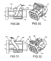
- Figures 29 - 32 show the manner in which the two connectors 104, 106 are mated.
- Figures 33-37 show the unmating steps.
- To mate the two connectors 104, 106 it is first necessary for an operator to push the two connectors 104, 106 into partial engagement. Since the header 104 will normally be fixed to an electrical component, and may be mounted on a fixed bulkhead or panel, this step will normally require the operator to grasp the plug connector 106, which will normally be attached to wires or on the end of a wire harness. The operator will align the two connectors and then push the plug connector 106 into partial engagement with the header connector 104. There will, of course, be no functional difference if the receptacle is a bulkhead mounted configuration attached to wires.
- auxiliary latch 196 will ride up and over the detent 224. (The inertial feature located opposite to the auxiliary latch 196 must also be overcome.) The end of the auxiliary contact 130 will engage the receptacle terminal 150. If the circuit to which either terminal 110, 150 is attached is live, some current will initially flow through the auxiliary contact 130, and there will be a make spark as the auxiliary contact 130 engages the receptacle terminal 150. A make spark is benign compared to a breaking arc and will not cause significant damage.
- the PTC conductive polymer 140 will also conduct since it will be in the ON or RESET state prior to mating. If the current is high enough the PTC conductive polymer 140 will trip to the OFF condition. If the initial current is not sufficient to trip the PTC conductive polymer 140, then the PTC conductive polymer 140 will remain in the ON state. The operator will not be able to push the connector 104, 106 to their fully mated configuration because the cam profiles for the lever mechanism 180 will prevent further movement of the connector unless the lever is rotated.
- lever arms 182 Just prior to engagement of the main contacts 112 with the receptacle terminal 150, the fingers 194 on lever arms 182 will engage the sloping surfaces 216 on the exterior of the header shroud 202 to force the lever arms 182 outward and free the lever arms 182 from abutting edges 168 of the plug housing sleeve 166.
- the lever 180 can now be rotated to its fully engaged position as shown in Figures 31 and 32 in which the main contacts 112 will be fully mated with the receptacle terminal 150.
- a make spark will also occur as the main contacts 112 engage the receptacle terminal 150.
- the make spark will not cause any significant damage because of its benign nature compared to a breaking arc. In any event, once there is a low resistance path established between the main contact blade sections 114 A, B and the receptacle terminal 150, only a small amount of current will be allowed to flow through the auxiliary contact 130 and the PTC conductive polymer 140.
- connection of the main contacts 114 A, B to the receptacle terminal 150 would sufficiently reduce the current through the PTC conductive polymer 140 to allow the PTC conductive polymer 140 to cool and reset to an ON state.
- the PTC conductive polymer will then be able to protect against an arc when unmating of the connectors 104, 106 breaks a live circuit. This cooling and recovery to the low resistance state occurs very quickly, on the order of seconds or less in typical applicable devices.
- the first step in the unmating procedure is to depress the release projection 184 to permit rotation of the mechanical assist lever 180.
- the arrow in Figure 31 shows the direction in which a force is applied to this release projection.
- the lever 180 can be rotated in a clockwise direction as shown in Figure 33. Movement of the lever 180 from the position shown in Figure 31 to the position shown in Figure 33 and finally to the position shown in Figure 35 will disengage the main contact 112 from the receptacle terminal 150. Referring to Figure 1, this will shift the main contact blade sections 114 A, B from Stage 0 through the Main Disconnect Zone (MDZ) to Stage 2.
- MDZ Main Disconnect Zone
- the inner detent 222 on the header housing 200 and a corresponding detent or raised surface on the interior of the plug connector sleeve 166 will also prevent the two connectors 104, 106 from staying in the MDZ where the contacts either remain in contact, or experience intermittent touching which could establish an arc between the main contact 112 and the receptacle terminal 150.
- There is another detent for the main contact that is a mirror image of detent 222 located on the bottom of the header.
- the unmentioned detent is on the opposite side and shifted off center to distribute the load evenly. This detent is important because one detent would create instability.If this time is prolonged the PTC conductive polymer 140 could switch to the OFF state and permit an arc to be developed.
- the PTC Opening Zone will last long enough for the PTC to open regardless of the current flowing through the connector when unmating begins.
- the current will be low enough so that a damaging arc will not be generated as the auxiliary contact 130 moves through the ADZ (auxiliary disconnect zone).
- ADZ auxiliary disconnect zone
- Figure 38 shows the damage that can result from arcing for a conventional contact that has been disconnected one time with a purely resistive load at 59 volts, 60 amperes without the use of the PTC resistor of the instant invention. Note the damage to the spring members in the mating connector.
- Figure 39 shows a similar contact that has been disconnected fifty times with a purely resistive load at 59 volts, 60 amperes using a PTC in accordance with this invention. Both mating contacts are undamaged. The auxiliary contact in the protected version is also undamaged since there was only leakage current flowing through the auxiliary when it separated from the mating contact.
- Figures 38 and 39 show the effects of the conductive polymer PTC device to prevent arcing damage when a connector assembly is used with a purely resistive load.
- Inductive loads can be expected to cause over-voltage spikes when the connectors are disconnected while high currents are flowing. If the PTC device can withstand those voltage spikes, the arc protection will work exactly as previously described. If the PTC device cannot withstand the voltage spikes, then it can be destroyed unless it is protected from those over-voltages by utilizing an over-voltage protection device such as an MOV, zener diodes or spark-gaps. Alternatively, the inductive load can have the over-voltage protection devices across it and there will again be no destructive over-voltage exposure for the PTC device.
- Figure 40 shows the manner in which a surge suppressor or over-voltage clamp 40 (such as a zener diode, MOV or spark gap) can be connected in parallel with the PTC device 402 in a protected arc-less connector assembly 404 according this invention including a main contact 406 and an auxiliary contact 408.
- the connector 404 is shown connected to a battery or power supply 410 and an inductive load 412.
- Figure 41 shows an alternative arrangement in which an arc-less connector 414 according to the invention, including a main contact 406, an auxiliary contact 408 and a PTC device 402, is connected to a battery or power supply 410 and a protected load 416 including an inductive load 406 and a surge suppressor or over-voltage clamp 400 (such as a zener diode, MOV or spark gap) are connected in parallel with each other.
- a surge suppressor or over-voltage clamp 400 such as a zener diode, MOV or spark gap
- Separation velocity is controlled in each of the representative embodiments of this invention by employing a two step unmating procedure that results in a sufficient time delay to allow the conductive polymer PTC device to turn OFF before the auxiliary contact is disengaged. Means are also provided in the preferred embodiment that will insure that the main contacts are quickly disconnected before the PTC member is able to switch to the OFF condition.
- the representative means discussed herein are not the only means of separation velocity control that can be employed.
- the unmating velocity of a manually operated electrical connector can be controlled in different ways. Also, if the load current range is limited, meaning that there is a minimum current that can flow, which is a significant percentage of the maximum current, the delay caused by the additional length of the auxiliary contact can be sufficient, causing a distinct 2-step disengagement to be unnecessary.
- FIGS 42A-42D shows a receptacle connector 304 and a mating plug connector 306 which includes a means for providing rapid unidirectional movement through the contact disconnect zones and the time delay between them with a single lever.
- This alternative lever configuration can provide unidirectional high velocity through the MDZ and the ADZ, while also providing a time delay between those zones without an additional latch.
- the high velocity is generated as the loaded cantilever beam 316 on the lever 308 pushes the plug pin 310 through the receptacle housing detents 312, 314 in a housing channel 318 as shown in Figures 42A and 42C.
- the time delay is caused when the cantilever beam 316 on the lever 308 relaxes after pushing the plug pin 310 through the first receptacle housing detent 312 and then is re-flexed or reloaded by continuing motion of the lever 308 until it can push the plug pin 310 through the second receptacle housing detent 314.
- a detent or spring release feature
- Pistons, or dashpot devices can provide controlled resistance that can slow velocity and additional latching mechanisms or levers can force momentary stops between the separation of the main and auxiliary contacts if necessary.
- Other means would also be apparent to one of ordinary skill in the art.
- This invention is also not limited to a conductive polymer PTC device.
- Other positive temperature coefficient resistance devices exist that could be substituted for the conductive polymer PTC devices or materials that are used in the preferred embodiments discussed herein.
- Metallic PTC devices are know to exist which could be employed in alternate embodiments that employ all of the basic elements of this invention.
- Other PT materials such as doped- BaTiO 3 might also be employed, although the expense of these various alternatives may prevent them from comprising an acceptable commercial alternative to the use of conductive polymer PTC devices and materials.
- Other alternative embodiments would be apparent to one of ordinary skill in the art. Therefore the invention, described herein in terms of representative preferred embodiment, is not limited to those representative embodiments, but is defined by the following claims.
Landscapes
- Details Of Connecting Devices For Male And Female Coupling (AREA)
- Connector Housings Or Holding Contact Members (AREA)
- Coupling Device And Connection With Printed Circuit (AREA)
Applications Claiming Priority (6)
| Application Number | Priority Date | Filing Date | Title |
|---|---|---|---|
| US30942401P | 2001-08-01 | 2001-08-01 | |
| US309424P | 2001-08-01 | ||
| US32411101P | 2001-09-21 | 2001-09-21 | |
| US324111P | 2001-09-21 | ||
| US22635 | 2001-12-17 | ||
| US10/022,635 US6659783B2 (en) | 2001-08-01 | 2001-12-17 | Electrical connector including variable resistance to reduce arcing |
Publications (3)
| Publication Number | Publication Date |
|---|---|
| EP1283565A2 true EP1283565A2 (de) | 2003-02-12 |
| EP1283565A3 EP1283565A3 (de) | 2004-11-10 |
| EP1283565B1 EP1283565B1 (de) | 2011-04-06 |
Family
ID=27361921
Family Applications (1)
| Application Number | Title | Priority Date | Filing Date |
|---|---|---|---|
| EP02255391A Expired - Lifetime EP1283565B1 (de) | 2001-08-01 | 2002-08-01 | Verbinder ohne Lichtbogen |
Country Status (7)
| Country | Link |
|---|---|
| US (1) | US6659783B2 (de) |
| EP (1) | EP1283565B1 (de) |
| JP (1) | JP4190822B2 (de) |
| KR (1) | KR100922694B1 (de) |
| BR (1) | BRPI0203036B1 (de) |
| CA (1) | CA2396082C (de) |
| DE (1) | DE60239654D1 (de) |
Cited By (4)
| Publication number | Priority date | Publication date | Assignee | Title |
|---|---|---|---|---|
| WO2015164189A1 (en) * | 2014-04-22 | 2015-10-29 | Tyco Electronics Corporation | Mezzanine receptacle connector |
| WO2018001681A1 (de) * | 2016-06-28 | 2018-01-04 | Phoenix Contact Gmbh & Co. Kg | Steckverbinder mit einem kontaktierungsabschnitt zur ableitung eines lichtbogens |
| WO2018025187A1 (en) * | 2016-08-01 | 2018-02-08 | Te Connectivity Corporaton | Power terminal for arcless power connector |
| WO2018025137A1 (en) * | 2016-08-01 | 2018-02-08 | Te Connectivity Corporation | Arcless power connector |
Families Citing this family (48)
| Publication number | Priority date | Publication date | Assignee | Title |
|---|---|---|---|---|
| US20030054683A1 (en) * | 2001-08-14 | 2003-03-20 | Bryan Lyle S. | Arc prevention circuits |
| US6636133B2 (en) * | 2001-09-14 | 2003-10-21 | Square D Company | PTC terminals |
| US6943661B2 (en) * | 2001-10-16 | 2005-09-13 | General Electric Company | Quick-connect positive temperature coefficient of resistance resistor/overload assembly and method |
| JP2003317870A (ja) * | 2002-04-23 | 2003-11-07 | Sumitomo Wiring Syst Ltd | コネクタ |
| US6790101B1 (en) | 2003-07-15 | 2004-09-14 | Molex Incorporated | Female terminal with sacrificial arc discharge contacts |
| KR100524290B1 (ko) | 2003-07-18 | 2005-10-26 | 권순목 | 분리형 분배로터와 이 분배로터를 채택한 수평식 로터분배기 |
| DE50312260D1 (de) * | 2003-10-07 | 2010-02-04 | Behr France Rouffach Sas | Heizungsanordnung mit PTC-Element, insbesondere für ein Kraftfahrzeug |
| US7149063B2 (en) * | 2004-01-20 | 2006-12-12 | Tyco Electronics Corporation | Apparatus, methods and articles of manufacture to minimize arcing in electrical connectors |
| TW200618418A (en) * | 2004-07-30 | 2006-06-01 | Kawamura Electric Inc | Power outlet |
| JP2006074872A (ja) * | 2004-08-31 | 2006-03-16 | Sumitomo Wiring Syst Ltd | 自動車用の電気接続箱 |
| US7104812B1 (en) * | 2005-02-24 | 2006-09-12 | Molex Incorporated | Laminated electrical terminal |
| KR100686844B1 (ko) * | 2005-07-25 | 2007-02-26 | 삼성에스디아이 주식회사 | Ptc소자를 구비한 이차전지 |
| US20070059973A1 (en) * | 2005-09-15 | 2007-03-15 | Tyco Electronics Corporation | Hot plug wire contact and connector assembly |
| CN101313444B (zh) * | 2005-11-23 | 2013-01-09 | 德雷格医疗系统股份有限公司 | 连接系统 |
| US20080076289A1 (en) * | 2006-09-11 | 2008-03-27 | Yueh-Hua Hsu Huang | Structure of Connnectors |
| DE102007003375B4 (de) * | 2007-01-23 | 2014-09-18 | Tyco Electronics Amp Gmbh | Elektrische Steckverbindung |
| KR100940510B1 (ko) | 2008-09-30 | 2010-02-10 | 주식회사 아이엔피 | 분리형 플러그를 가지는 헤어드라이기의 아크방지장치 |
| US8213134B2 (en) * | 2008-12-30 | 2012-07-03 | International Business Machines Corporation | Apparatus, system, and method to prevent smoke in a power supply powered by a current limited source |
| US8215992B1 (en) | 2010-12-20 | 2012-07-10 | Tyco Electronics Corporation | Electrical connector having a resistor |
| JP6054599B2 (ja) * | 2011-08-11 | 2016-12-27 | 富士通コンポーネント株式会社 | スイッチ及びコネクタ |
| JP5858745B2 (ja) * | 2011-11-21 | 2016-02-10 | 矢崎総業株式会社 | 電源回路遮断装置 |
| US8939787B2 (en) * | 2012-08-27 | 2015-01-27 | Schneider Electric USA, Inc. | Dual material ground clip for a busway plug in unit |
| US9548553B2 (en) * | 2013-03-15 | 2017-01-17 | Lear Corporation | Terminal with front end protection |
| US20150180179A1 (en) * | 2013-12-19 | 2015-06-25 | Tyco Electronics Amp Korea Ltd | Connector Assembly |
| TWI535134B (zh) | 2014-01-02 | 2016-05-21 | 萬國商業機器公司 | 電力互連裝置及插座結構及提供直流電的方法 |
| US20160109530A1 (en) * | 2014-10-21 | 2016-04-21 | Analog Devices Technology | Combination of a battery stack and a battery monitor, and a method of connecting a battery monitor to a stack of batteries |
| JP6342346B2 (ja) * | 2015-02-23 | 2018-06-13 | 株式会社日立製作所 | 電力変換装置 |
| US9647444B2 (en) | 2015-06-16 | 2017-05-09 | Hamilton Sundstrand Corporation | Variable threshold current limiting circuit |
| US9472892B1 (en) | 2015-07-16 | 2016-10-18 | Eaton Corporation | Power connector, and electrical connection element and assembly method therefor |
| US9666977B2 (en) | 2015-07-29 | 2017-05-30 | Abb Schweiz Ag | Direct current socket with direct current arc protection |
| US10483693B2 (en) | 2015-09-24 | 2019-11-19 | Abb Schweiz Ag | Sliding contact assembly for accelerating relative separation speed between plug contacts and socket outlet contacts |
| EP3211722B1 (de) * | 2016-02-23 | 2020-04-22 | TE Connectivity Germany GmbH | Kontaktbolzen und kontaktanordnung insbesondere für autotechnologie |
| DE102016104739A1 (de) * | 2016-03-15 | 2017-09-21 | Endress + Hauser Flowtec Ag | Feldgerät der Mess- und Automatisierungstechnik |
| US10074944B2 (en) * | 2016-03-21 | 2018-09-11 | Littelfuse, Inc. | Arc suppression connector |
| CN107623217B (zh) * | 2016-12-29 | 2023-12-12 | 湖南格瑞普新能源有限公司 | 能过大电流的电插件 |
| EP3389148B1 (de) | 2017-04-10 | 2020-09-02 | Yazaki Europe Ltd. | Elektrosteckverbinderanordnung |
| FR3067870B1 (fr) * | 2017-06-16 | 2021-01-01 | Schneider Electric Ind Sas | Appareil de protection electrique comportant un dispositif limiteur de courant |
| US10446974B2 (en) | 2017-09-20 | 2019-10-15 | Te Connectivity Corporation | Electrical connector having an arc suppression element |
| CN107834324A (zh) * | 2017-10-31 | 2018-03-23 | 恒安科技(中山)有限公司 | 一种防爆连接器 |
| JP2019091610A (ja) * | 2017-11-14 | 2019-06-13 | 住友電装株式会社 | コネクタ |
| US10505312B2 (en) | 2018-02-07 | 2019-12-10 | Smiths Interconnect Americas, Inc. | Hot mate contact system |
| JP6793683B2 (ja) * | 2018-06-14 | 2020-12-02 | 矢崎総業株式会社 | レバー式コネクタ |
| CN112448218B (zh) * | 2019-08-27 | 2022-05-03 | 胡连电子(南京)有限公司 | 一种防止带电拔插的连接器 |
| TWI730401B (zh) * | 2019-09-09 | 2021-06-11 | 一諾科技股份有限公司 | 交流電力輸入插座 |
| KR20220123641A (ko) * | 2019-12-05 | 2022-09-08 | 수조우 리텔퓨즈 오브이에스 컴퍼니 리미티드 | 역접속 보호를 구비한 릴레이 어셈블리 |
| US10992073B1 (en) * | 2019-12-20 | 2021-04-27 | Lear Corporation | Electrical terminal assembly with increased contact area |
| CN114122807B (zh) * | 2021-10-22 | 2024-04-16 | 中航光电科技股份有限公司 | 一种可自锁的连接器 |
| WO2023200426A1 (en) * | 2022-04-11 | 2023-10-19 | Ideal Industries, Inc. | Electrical connectors with arc protection |
Citations (2)
| Publication number | Priority date | Publication date | Assignee | Title |
|---|---|---|---|---|
| US4681549A (en) * | 1982-07-14 | 1987-07-21 | Northern Telecom Limited | Printed circuit board edge connection arrangements |
| US6072673A (en) * | 1998-11-19 | 2000-06-06 | Square D Company | Medium to high voltage load circuit interrupters including metal resistors having a positive temperature coefficient of resistivity (PTC elements) |
Family Cites Families (38)
| Publication number | Priority date | Publication date | Assignee | Title |
|---|---|---|---|---|
| GB1214659A (en) | 1967-02-27 | 1970-12-02 | Mitsubishi Electric Corp | A current limiting device |
| US3956723A (en) | 1974-04-29 | 1976-05-11 | Square D Company | Current limiting circuit breaker |
| US4178618A (en) | 1974-04-29 | 1979-12-11 | Square D Company | Current limiting circuit breaker |
| US3943473A (en) | 1974-04-29 | 1976-03-09 | Square D Company | Current limiting circuit breaker |
| US4079440A (en) * | 1977-01-19 | 1978-03-14 | Hitachi, Ltd. | Printed circuit board capable of being inserted and withdrawn on on-line status |
| US4198024A (en) * | 1977-11-10 | 1980-04-15 | Burroughs Corporation | Printed circuit card holder |
| US5049850A (en) | 1980-04-21 | 1991-09-17 | Raychem Corporation | Electrically conductive device having improved properties under electrical stress |
| US5178797A (en) | 1980-04-21 | 1993-01-12 | Raychem Corporation | Conductive polymer compositions having improved properties under electrical stress |
| US4438472A (en) | 1982-08-09 | 1984-03-20 | Ibm Corporation | Active arc suppression for switching of direct current circuits |
| US4659160A (en) * | 1982-12-21 | 1987-04-21 | Legrand | Electrical connector socket suitable for use in explosive atomsphere |
| US4583146A (en) | 1984-10-29 | 1986-04-15 | General Electric Company | Fault current interrupter |
| FR2606929B1 (fr) | 1986-11-14 | 1989-02-10 | Telemecanique Electrique | Dispositif interrupteur pour appareil de protection |
| JPH0630290B2 (ja) * | 1987-05-15 | 1994-04-20 | 株式会社村田製作所 | 可変抵抗器 |
| JPH0320978A (ja) * | 1989-06-19 | 1991-01-29 | Hitachi Ltd | コネクタ |
| JPH0325870A (ja) * | 1989-06-22 | 1991-02-04 | Canon Inc | コネクタ |
| US5247277A (en) * | 1990-02-14 | 1993-09-21 | Raychem Corporation | Electrical devices |
| JPH042467U (de) * | 1990-04-19 | 1992-01-10 | ||
| JPH05101907A (ja) | 1991-03-30 | 1993-04-23 | Toshiba Corp | 電力用遮断器および電力用抵抗体 |
| JPH04127982U (ja) * | 1991-05-14 | 1992-11-20 | 本田技研工業株式会社 | 離脱防止手段を備えたカプラ |
| FR2677485A1 (fr) | 1991-06-07 | 1992-12-11 | Stopcircuit Sa | Appareil de coupure en charge pour circuit electrique. |
| US5378407A (en) | 1992-06-05 | 1995-01-03 | Raychem Corporation | Conductive polymer composition |
| US5176528A (en) | 1992-06-11 | 1993-01-05 | Molex Incorporated | Pin and socket electrical connnector assembly |
| US5629658A (en) | 1992-08-18 | 1997-05-13 | Chen; William W. | Methods of arc suppression and circuit breakers with electronic alarmers |
| DE69414712T2 (de) | 1993-08-23 | 1999-07-29 | Raychem Corp | Verwendung von kaltleiteranordnungen in kabelbäumen |
| FR2714520B1 (fr) * | 1993-12-24 | 1996-01-19 | Telemecanique | Appareil électrique interrupteur à contacts séparables. |
| US5428195A (en) | 1994-01-31 | 1995-06-27 | General Electric Company | Current limiter unit for molded case circuit breakers |
| JPH07335329A (ja) * | 1994-06-13 | 1995-12-22 | Fujitsu Denso Ltd | 突入電流制限接続器 |
| US5945903A (en) | 1995-06-07 | 1999-08-31 | Littelfuse, Inc. | Resettable automotive circuit protection device with female terminals and PTC element |
| US5737160A (en) | 1995-09-14 | 1998-04-07 | Raychem Corporation | Electrical switches comprising arrangement of mechanical switches and PCT device |
| US5864458A (en) | 1995-09-14 | 1999-01-26 | Raychem Corporation | Overcurrent protection circuits comprising combinations of PTC devices and switches |
| US5689395A (en) | 1995-09-14 | 1997-11-18 | Raychem Corporation | Overcurrent protection circuit |
| US5983298A (en) | 1995-11-20 | 1999-11-09 | Allen-Bradley Company, Llc | Industrial controller permitting removal and insertion of circuit cards while under power |
| FR2742916B1 (fr) * | 1995-12-21 | 1998-01-16 | Schneider Electric Sa | Dispositif electrique a commutation d'arc |
| US6078160A (en) | 1997-10-31 | 2000-06-20 | Cilluffo; Anthony | Bidirectional DC motor control circuit including overcurrent protection PTC device and relay |
| US5909065A (en) * | 1997-12-23 | 1999-06-01 | Dsc Telecom L.P. | Multi-stage precharging system to limit power supply transients when printed circuit boards are plugged in |
| US6072680A (en) | 1998-07-28 | 2000-06-06 | Airpax Corporation, Llc | High temperature lockout and thermostat |
| US6217356B1 (en) | 1999-03-30 | 2001-04-17 | The Whitaker Corporation | Electrical terminal with arc arresting region |
| US20020018332A1 (en) * | 2000-07-04 | 2002-02-14 | Matthias Kroeker | Arrangement having a contact element which can be brought into contact with another contact element |
-
2001
- 2001-12-17 US US10/022,635 patent/US6659783B2/en not_active Expired - Lifetime
-
2002
- 2002-07-31 CA CA2396082A patent/CA2396082C/en not_active Expired - Fee Related
- 2002-07-31 BR BRPI0203036A patent/BRPI0203036B1/pt not_active IP Right Cessation
- 2002-08-01 JP JP2002225297A patent/JP4190822B2/ja not_active Expired - Fee Related
- 2002-08-01 KR KR1020020045613A patent/KR100922694B1/ko active IP Right Grant
- 2002-08-01 DE DE60239654T patent/DE60239654D1/de not_active Expired - Lifetime
- 2002-08-01 EP EP02255391A patent/EP1283565B1/de not_active Expired - Lifetime
Patent Citations (2)
| Publication number | Priority date | Publication date | Assignee | Title |
|---|---|---|---|---|
| US4681549A (en) * | 1982-07-14 | 1987-07-21 | Northern Telecom Limited | Printed circuit board edge connection arrangements |
| US6072673A (en) * | 1998-11-19 | 2000-06-06 | Square D Company | Medium to high voltage load circuit interrupters including metal resistors having a positive temperature coefficient of resistivity (PTC elements) |
Cited By (12)
| Publication number | Priority date | Publication date | Assignee | Title |
|---|---|---|---|---|
| WO2015164189A1 (en) * | 2014-04-22 | 2015-10-29 | Tyco Electronics Corporation | Mezzanine receptacle connector |
| US9293845B2 (en) | 2014-04-22 | 2016-03-22 | Tyco Electronics Corporation | Mezzanine receptacle connector |
| WO2018001681A1 (de) * | 2016-06-28 | 2018-01-04 | Phoenix Contact Gmbh & Co. Kg | Steckverbinder mit einem kontaktierungsabschnitt zur ableitung eines lichtbogens |
| LU93125B1 (de) * | 2016-06-28 | 2018-01-24 | Phoenix Contact Gmbh & Co Kg Intellectual Property Licenses & Standards | Steckverbinder mit einem Kontaktierungsabschnitt zur Ableitung eines Lichtbogens |
| KR20190020138A (ko) * | 2016-06-28 | 2019-02-27 | 피닉스 컨택트 게엠베하 & 컴퍼니 카게 | 전기 아크를 우회시키기 위한 접촉 부분을 갖는 플러그 커넥터 |
| CN109417245A (zh) * | 2016-06-28 | 2019-03-01 | 菲尼克斯电气公司 | 具有用于导出电弧的接触区段的插式连接器 |
| US10784617B2 (en) | 2016-06-28 | 2020-09-22 | Phoenix Contact Gmbh & Co. Kg | Plug connector with a contacting portion for diverting an electric arc |
| CN109417245B (zh) * | 2016-06-28 | 2021-06-01 | 菲尼克斯电气公司 | 具有用于导出电弧的接触区段的插式连接器 |
| WO2018025187A1 (en) * | 2016-08-01 | 2018-02-08 | Te Connectivity Corporaton | Power terminal for arcless power connector |
| WO2018025137A1 (en) * | 2016-08-01 | 2018-02-08 | Te Connectivity Corporation | Arcless power connector |
| US10020613B2 (en) | 2016-08-01 | 2018-07-10 | Te Connectivity Corporation | Power terminal for arcless power connector |
| US10148034B2 (en) | 2016-08-01 | 2018-12-04 | Te Connectivity Corporation | Arcless power connector |
Also Published As
| Publication number | Publication date |
|---|---|
| BR0203036A (pt) | 2003-05-27 |
| DE60239654D1 (de) | 2011-05-19 |
| KR100922694B1 (ko) | 2009-10-20 |
| US6659783B2 (en) | 2003-12-09 |
| KR20030013312A (ko) | 2003-02-14 |
| EP1283565A3 (de) | 2004-11-10 |
| US20030027447A1 (en) | 2003-02-06 |
| JP2003077563A (ja) | 2003-03-14 |
| EP1283565B1 (de) | 2011-04-06 |
| CA2396082A1 (en) | 2003-02-01 |
| CA2396082C (en) | 2010-02-16 |
| JP4190822B2 (ja) | 2008-12-03 |
| BRPI0203036B1 (pt) | 2017-02-14 |
Similar Documents
| Publication | Publication Date | Title |
|---|---|---|
| EP1283565B1 (de) | Verbinder ohne Lichtbogen | |
| US10148034B2 (en) | Arcless power connector | |
| EP2486630B1 (de) | Verbinderanordnung mit mehrstufiger arretierungssequenz | |
| RU2586994C2 (ru) | Устройство защиты от перенапряжения, содержащее по меньшей мере один разрядник | |
| US4978311A (en) | Electrical connector having connector-operable shorting bar | |
| US10014098B2 (en) | Surge protection device, comprising at least one surge arrester and one short-circuit switching device which is connected in parallel with the surge arrester, can be thermally tripped and is spring-pretensioned | |
| CN110571567A (zh) | 分阶段释放的电连接器组件 | |
| WO2022000353A1 (zh) | 一种底座、带底座的断路器和配电设备 | |
| JP2003141973A (ja) | 電源遮断時における保護装置 | |
| US10020613B2 (en) | Power terminal for arcless power connector | |
| CA1065929A (en) | Cut-out switch having load interrupter | |
| CN108400072B (zh) | 单级断路器 | |
| US20160042898A1 (en) | Ventilated circuit breakers, ventilated circuit breaker housings, and operational methods | |
| US6485318B1 (en) | Electrical shuttle connector | |
| US11081307B2 (en) | Electrical power supply disconnector for a protection module and protection module including such a disconnector | |
| CN114220713A (zh) | 断路保护装置、动力电池系统及电动汽车 | |
| ES2361493T3 (es) | Conector eléctrico sin arco. | |
| EP3467961A1 (de) | Verbinder | |
| JP7311294B2 (ja) | 電源回路遮断装置 | |
| CN110676118B (zh) | 开关的过热破坏式断电方法 | |
| CN109417245B (zh) | 具有用于导出电弧的接触区段的插式连接器 | |
| CN101038831B (zh) | 电路断路器 | |
| CN117833179A (zh) | 一种接触式双脱扣型瞬态电压抑制器 | |
| KR20030075856A (ko) | 플러그탈착기능에 전원개폐기능이 부가된 콘센트 | |
| JPH06338362A (ja) | 消弧手段を備えた分離可能なコネクタ |
Legal Events
| Date | Code | Title | Description |
|---|---|---|---|
| PUAI | Public reference made under article 153(3) epc to a published international application that has entered the european phase |
Free format text: ORIGINAL CODE: 0009012 |
|
| AK | Designated contracting states |
Designated state(s): AT BE BG CH CY CZ DE DK EE ES FI FR GB GR IE IT LI LU MC NL PT SE SK TR |
|
| AX | Request for extension of the european patent |
Extension state: AL LT LV MK RO SI |
|
| PUAL | Search report despatched |
Free format text: ORIGINAL CODE: 0009013 |
|
| AK | Designated contracting states |
Kind code of ref document: A3 Designated state(s): AT BE BG CH CY CZ DE DK EE ES FI FR GB GR IE IT LI LU MC NL PT SE SK TR |
|
| AX | Request for extension of the european patent |
Extension state: AL LT LV MK RO SI |
|
| 17P | Request for examination filed |
Effective date: 20050506 |
|
| AKX | Designation fees paid |
Designated state(s): DE ES FR GB IT |
|
| 17Q | First examination report despatched |
Effective date: 20080424 |
|
| GRAP | Despatch of communication of intention to grant a patent |
Free format text: ORIGINAL CODE: EPIDOSNIGR1 |
|
| GRAS | Grant fee paid |
Free format text: ORIGINAL CODE: EPIDOSNIGR3 |
|
| GRAA | (expected) grant |
Free format text: ORIGINAL CODE: 0009210 |
|
| AK | Designated contracting states |
Kind code of ref document: B1 Designated state(s): DE ES FR GB IT |
|
| REG | Reference to a national code |
Ref country code: GB Ref legal event code: FG4D |
|
| REF | Corresponds to: |
Ref document number: 60239654 Country of ref document: DE Date of ref document: 20110519 Kind code of ref document: P |
|
| REG | Reference to a national code |
Ref country code: DE Ref legal event code: R096 Ref document number: 60239654 Country of ref document: DE Effective date: 20110519 |
|
| REG | Reference to a national code |
Ref country code: ES Ref legal event code: FG2A Ref document number: 2361493 Country of ref document: ES Kind code of ref document: T3 Effective date: 20110617 |
|
| PLBE | No opposition filed within time limit |
Free format text: ORIGINAL CODE: 0009261 |
|
| STAA | Information on the status of an ep patent application or granted ep patent |
Free format text: STATUS: NO OPPOSITION FILED WITHIN TIME LIMIT |
|
| 26N | No opposition filed |
Effective date: 20120110 |
|
| REG | Reference to a national code |
Ref country code: DE Ref legal event code: R097 Ref document number: 60239654 Country of ref document: DE Effective date: 20120110 |
|
| REG | Reference to a national code |
Ref country code: FR Ref legal event code: PLFP Year of fee payment: 15 |
|
| REG | Reference to a national code |
Ref country code: FR Ref legal event code: PLFP Year of fee payment: 16 |
|
| REG | Reference to a national code |
Ref country code: FR Ref legal event code: PLFP Year of fee payment: 17 |
|
| REG | Reference to a national code |
Ref country code: FR Ref legal event code: CD Owner name: TYCO ELECTRONICS CORPORATION, US Effective date: 20180626 |
|
| REG | Reference to a national code |
Ref country code: ES Ref legal event code: PC2A Owner name: TE CONNECTIVITY CORPORATION Effective date: 20181005 |
|
| REG | Reference to a national code |
Ref country code: DE Ref legal event code: R082 Ref document number: 60239654 Country of ref document: DE Representative=s name: MARKS & CLERK (LUXEMBOURG) LLP, LU Ref country code: DE Ref legal event code: R081 Ref document number: 60239654 Country of ref document: DE Owner name: TE CONNECTIVITY CORPORATION, BERWYN, US Free format text: FORMER OWNER: TYCO ELECTRONICS CORP., MIDDLETOWN, PA., US |
|
| PGFP | Annual fee paid to national office [announced via postgrant information from national office to epo] |
Ref country code: ES Payment date: 20180801 Year of fee payment: 17 Ref country code: IT Payment date: 20180823 Year of fee payment: 17 |
|
| PGFP | Annual fee paid to national office [announced via postgrant information from national office to epo] |
Ref country code: GB Payment date: 20190731 Year of fee payment: 18 |
|
| PG25 | Lapsed in a contracting state [announced via postgrant information from national office to epo] |
Ref country code: IT Free format text: LAPSE BECAUSE OF NON-PAYMENT OF DUE FEES Effective date: 20190801 |
|
| REG | Reference to a national code |
Ref country code: ES Ref legal event code: FD2A Effective date: 20210105 |
|
| PG25 | Lapsed in a contracting state [announced via postgrant information from national office to epo] |
Ref country code: ES Free format text: LAPSE BECAUSE OF NON-PAYMENT OF DUE FEES Effective date: 20190802 |
|
| GBPC | Gb: european patent ceased through non-payment of renewal fee |
Effective date: 20200801 |
|
| PGFP | Annual fee paid to national office [announced via postgrant information from national office to epo] |
Ref country code: FR Payment date: 20210611 Year of fee payment: 20 |
|
| PG25 | Lapsed in a contracting state [announced via postgrant information from national office to epo] |
Ref country code: GB Free format text: LAPSE BECAUSE OF NON-PAYMENT OF DUE FEES Effective date: 20200801 |
|
| PGFP | Annual fee paid to national office [announced via postgrant information from national office to epo] |
Ref country code: DE Payment date: 20210630 Year of fee payment: 20 |
|
| REG | Reference to a national code |
Ref country code: DE Ref legal event code: R071 Ref document number: 60239654 Country of ref document: DE |