EP1282342A2 - Freischwingende Schaltungsanordnung - Google Patents
Freischwingende Schaltungsanordnung Download PDFInfo
- Publication number
- EP1282342A2 EP1282342A2 EP02011693A EP02011693A EP1282342A2 EP 1282342 A2 EP1282342 A2 EP 1282342A2 EP 02011693 A EP02011693 A EP 02011693A EP 02011693 A EP02011693 A EP 02011693A EP 1282342 A2 EP1282342 A2 EP 1282342A2
- Authority
- EP
- European Patent Office
- Prior art keywords
- switching element
- control
- circuit
- circuit arrangement
- capacitance
- Prior art date
- Legal status (The legal status is an assumption and is not a legal conclusion. Google has not performed a legal analysis and makes no representation as to the accuracy of the status listed.)
- Granted
Links
Images



Classifications
-
- H—ELECTRICITY
- H05—ELECTRIC TECHNIQUES NOT OTHERWISE PROVIDED FOR
- H05B—ELECTRIC HEATING; ELECTRIC LIGHT SOURCES NOT OTHERWISE PROVIDED FOR; CIRCUIT ARRANGEMENTS FOR ELECTRIC LIGHT SOURCES, IN GENERAL
- H05B41/00—Circuit arrangements or apparatus for igniting or operating discharge lamps
- H05B41/14—Circuit arrangements
- H05B41/26—Circuit arrangements in which the lamp is fed by power derived from DC by means of a converter, e.g. by high-voltage DC
- H05B41/28—Circuit arrangements in which the lamp is fed by power derived from DC by means of a converter, e.g. by high-voltage DC using static converters
- H05B41/282—Circuit arrangements in which the lamp is fed by power derived from DC by means of a converter, e.g. by high-voltage DC using static converters with semiconductor devices
- H05B41/2825—Circuit arrangements in which the lamp is fed by power derived from DC by means of a converter, e.g. by high-voltage DC using static converters with semiconductor devices by means of a bridge converter in the final stage
-
- Y—GENERAL TAGGING OF NEW TECHNOLOGICAL DEVELOPMENTS; GENERAL TAGGING OF CROSS-SECTIONAL TECHNOLOGIES SPANNING OVER SEVERAL SECTIONS OF THE IPC; TECHNICAL SUBJECTS COVERED BY FORMER USPC CROSS-REFERENCE ART COLLECTIONS [XRACs] AND DIGESTS
- Y02—TECHNOLOGIES OR APPLICATIONS FOR MITIGATION OR ADAPTATION AGAINST CLIMATE CHANGE
- Y02B—CLIMATE CHANGE MITIGATION TECHNOLOGIES RELATED TO BUILDINGS, e.g. HOUSING, HOUSE APPLIANCES OR RELATED END-USER APPLICATIONS
- Y02B20/00—Energy efficient lighting technologies, e.g. halogen lamps or gas discharge lamps
-
- Y—GENERAL TAGGING OF NEW TECHNOLOGICAL DEVELOPMENTS; GENERAL TAGGING OF CROSS-SECTIONAL TECHNOLOGIES SPANNING OVER SEVERAL SECTIONS OF THE IPC; TECHNICAL SUBJECTS COVERED BY FORMER USPC CROSS-REFERENCE ART COLLECTIONS [XRACs] AND DIGESTS
- Y10—TECHNICAL SUBJECTS COVERED BY FORMER USPC
- Y10S—TECHNICAL SUBJECTS COVERED BY FORMER USPC CROSS-REFERENCE ART COLLECTIONS [XRACs] AND DIGESTS
- Y10S315/00—Electric lamp and discharge devices: systems
- Y10S315/05—Starting and operating circuit for fluorescent lamp
-
- Y—GENERAL TAGGING OF NEW TECHNOLOGICAL DEVELOPMENTS; GENERAL TAGGING OF CROSS-SECTIONAL TECHNOLOGIES SPANNING OVER SEVERAL SECTIONS OF THE IPC; TECHNICAL SUBJECTS COVERED BY FORMER USPC CROSS-REFERENCE ART COLLECTIONS [XRACs] AND DIGESTS
- Y10—TECHNICAL SUBJECTS COVERED BY FORMER USPC
- Y10S—TECHNICAL SUBJECTS COVERED BY FORMER USPC CROSS-REFERENCE ART COLLECTIONS [XRACs] AND DIGESTS
- Y10S315/00—Electric lamp and discharge devices: systems
- Y10S315/07—Starting and control circuits for gas discharge lamp using transistors
Definitions
- the present invention relates to a freely oscillating circuit arrangement for operating a load with at least one switching element, a free-wheeling diode, to the main current direction of the at least one switching element is connected in anti-parallel, a load circuit and a control resonant circuit, the at least one tax inductance and at least one own capacitance of the at least one switching element.
- FIG. 1 there can be based on the principle from which this circuit works can be seen: one arranged in the load circuit Inductor L2, in the present case the lamp choke, has two auxiliary windings HW1 and HW2 coupled, the auxiliary winding HW1 in the control circuit a first switching element T1, the auxiliary winding HW2 in Control resonant circuit of a second switching element T2 is arranged.
- the load circuit Inductor L2 in the present case the lamp choke, has two auxiliary windings HW1 and HW2 coupled, the auxiliary winding HW1 in the control circuit a first switching element T1, the auxiliary winding HW2 in Control resonant circuit of a second switching element T2 is arranged.
- the object of the present invention is therefore that of the generic type free-floating circuit arrangement to develop such that the maintenance of an oscillation of the vibration is made possible without that this involves an electromagnetic coupling of components of the load circuit with components of the control circuit would be necessary.
- the at least one Switching element a control electrode, a working electrode and a reference electrode has, wherein between the control electrode and the working electrode a capacitance acts, which is coupled to the control circuit is that due to the charge and discharge current of this capacity, energy in the Control resonant circuit is fed, the circuit arrangement none Components for feeding energy into the control circuit has electromagnetic coupling.
- the invention is based on the finding that the maintenance of Vibration necessary energy via a capacitance to the control circuit can be supplied. An expensive, often custom-made Transformer is no longer necessary.
- Another advantage of the circuit arrangement according to the invention is in that the circuit arrangement with a smaller number of Components can be realized.
- the one switching element a Miller capacitance
- the one between the control electrode and the capacitance acting on the working electrode of the switching element is the Miller capacitance of the at least one switching element.
- Miller capacitances occur, for example, in field effect transistors.
- the Miller capacity of the minimum one switching element alone is enough to maintain the control circuit to supply the vibration with energy. Should be the Miller capacity alone is not enough, an additional discrete capacity can be connected in parallel become.
- control resonant circuit and the Miller capacitance to coordinate the at least one switching element with one another in such a way that the oscillation of the control resonant circuit is caused solely by the Charge and discharge current of the Miller capacitance of the at least one switching element is maintained.
- the intrinsic capacitance of the at least one switching element can be between Control and reference electrode used existing input capacity become.
- the circuit arrangement according to the invention preferably has a first and a second switching element, the first and the second switching element are complementary and with a common control circuit are coupled.
- the complementary version of the switching elements enables the use of a common control circuit for both switching elements. It is preferred if each switching element a control electrode, a working electrode and a reference electrode has, wherein the control electrodes together to form a first connection point and the reference electrodes to form a second connection point are interconnected, the control inductance coupled between the first and the second connection point is.
- the circuit arrangement is a has first and a second switching element, which are of the same type, wherein the first switching element with a first control circuit and that second switching element is coupled to a second control resonant circuit.
- each switching element has a control electrode, has a working electrode and a reference electrode, the reference electrode of the first switching element with the working electrode of the second Switching element is connected and the respective control inductance between the respective control and reference electrode of the respective switching element is coupled.
- the first and the second switching element are preferably in a half-bridge arrangement arranged.
- the load is preferably an illuminant, preferably a low-pressure discharge lamp.
- illuminant preferably a low-pressure discharge lamp.
- circuit for other types of Use loads.
- the input capacitance of the at least one switching element dimensioned unfavorably for a realization of the circuit arrangement is, it is preferred the input capacity of the at least one Switching element to connect a discrete additional capacity in parallel. This possibility results in further degrees of freedom for dimensioning of the control circuit.
- the load circuit preferably has a series resonant circuit with an inductance, a capacity connected in parallel to the load and at least one decoupling capacity on.
- the inductance is preferred as current limiting and Dimensioned resonance inductance.
- the at least one switching element is preferably a bipolar transistor or a MOS field effect transistor.
- the body diode can be implemented with at least one MOS field effect transistor of the MOS field effect transistor the anti-parallel connected freewheeling diode realize.
- the at least one switching element is implemented a discrete diode is to be provided as a freewheeling diode as the bipolar transistor.
- the ballast shown in FIG. 1 has a mains connection L, N, which is connected via a fuse Si to a rectifier comprising four diodes D1, D2, D3, D4.
- the DC voltage smoothed by a capacitor C1 is made available to the free-swinging circuit arrangement via a filter with an inductance L1 and a capacitor C2 as a so-called intermediate circuit voltage U z . Due to the voltage U z , the capacitor C3 is charged via the resistors R1 and R2.
- the circuit further comprises two MOS field-effect transistors T1, T2, the drain connection of transistor T1 being connected to the plus connection of capacitor C2, the drain connection of transistor T2 being connected to the minus connection of capacitor C2.
- connection point VP1 The source connections of the two transistors T1, T2 are connected to one another to form a connection point VP1, the connection point VP1 being connected to the plus-side connection of the capacitor C3.
- the minus side connection of the capacitor C3 is connected to ground via a diode D5 and a resistor R3, the diode D5 and the resistor R3 ensuring that the capacitor C3 is discharged during operation of the circuit arrangement, that is to say when the transistor T2 is turned on is so that the diac, which is connected between the minus-side connection of the capacitor C3 and the two gate connections of the two transistors T1, T2, does not ignite in a disturbing manner during the operation of the circuit arrangement.
- the series connection of an inductor L2 and a resistor R4 is arranged between the connection point VP1 and the interconnected gate connections of the transistors T1, T2.
- the series connection of a resistor R5 and a capacitor C4 is arranged on the one hand between the drain connection of the transistor T1 and the connection point VP1, the series connection of the series circuit comprising a capacitor C5, the illuminant La and the lamp inductor L3 being connected in parallel, the illuminant La in turn, a capacitor C5 is connected in parallel.
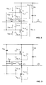
- FIG. 2 shows a section of the ballast from FIG. 1, the transistor capacitances being shown in broken lines.
- the respective Miller capacitance C M, T1 or C M, T2 is arranged between the respective gate and the respective drain connection. Between the respective gate connection and the respective source connection, the respective input capacitance C E, T1 or C E, T2 arranged, while the respective output capacitance C A, T1 or C A, T2 is arranged between the respective drain and the respective source connection.
- FIG. 3 shows a preferred possibility of this to enlarge.
- a capacitance C MZ is connected in parallel to the Miller capacitances C M, T1 , C M, T2
- a capacitance C EZ is connected in parallel to the input capacitances C E, T1 , C E, T2 .
- Figure 4 shows snapshots of the current flows in the circuit section of Figure 2 in chronological order.
- Figure 5 shows the course over time of various sizes of the circuit section from Figure 2 shown with reference to the voltages shown in Figure 2.
- the starting point is a DC voltage present across capacitor C2, based on which capacitor C3 is charged via resistors R1, R2. Due to the voltage rise above C3, the voltage applied to the diac also increases. If this exceeds the trigger threshold of the diac, the diac switches on, as a result of which a negative voltage pulse reaches the two gate connections of the complementary transistors T1 and T2. As a result, the capacities C M, T1 , C E, T1 C E, T2 are charged, while the capacitance C M, T2 is discharged. The current flow shown in FIG. 4a is established.
- the transistor T2 opens, see the current flow I ST2 in the time segment 4b in FIG. 5.
- a current begins in the load circuit via the capacitor C5, the capacitor C6 as well as the inductance L3 to flow.
- the current I ST2 which increases in amount, flows counter to the voltage direction U CA, T2 defined in FIG. 2 and thus has a negative sign.
- the negative voltage pulse at the gate electrode at the same time causes a rise in a control current I L2 through the inductance L2 which for the most part recharges the two input capacitances C E, T1 , C E, T2 of the transistors T1, T2.
- the current I L2 counteracts the voltage supplied by the diac, so that the previously negative gate voltage is reduced.
- the beginning of the period 4c is characterized in that after falling below the threshold voltage of the transistor T2, the latter shoots and the load current impressed in the inductance L3 now flows through the resistor R5 and discharges the capacitor C4. Simultaneously with the change in the voltage across the capacitor C4, the voltage across the Miller capacitances C M, T1 , C M, T2 of the two transistors T1, T2 also changes. In particular, this places the connection point of the two source electrodes almost at the voltage U z , this voltage swing being fully supported by the Miller capacitances C M, T1 , C M, T2 .
- period 4d The beginning of period 4d is characterized in that after the drain-source voltage at transistor T1 drops, its inner free-wheeling diode becomes conductive and thus takes over the main part of the current of inductor L3. As soon as the majority of the load current flows through the freewheeling diode of the transistor T1, see I ST1 in FIG. 5, the recharging processes of the Miller capacitors C M, T1 , C M, T2 are largely completed.
- the current impressed in the inductance L2 now mainly charges the two input capacitances C E, T1 , C E, T2 of the two transistors T1, T2 and initially causes the gate voltage to drop further to zero and finally increases to positive voltage values. After exceeding the threshold voltage of the transistor T1, it is switched on.
- the current impressed in the inductance L2 decays from T1 to zero during the single phase, as a result of which the beginning of the period 4e is marked.
- the input capacitances C E, T1 and C E, T2 of the two transistors T1, T2 are charged accordingly, so that the current can now flow from the charged capacitances to the gate circuit L2, R4 (just as in the load circuit, this also occurs in the control circuit a current reversal).
- the control current I L2 now flowing in the opposite direction through the inductor L2 counteracts the still positive gate voltage.
- the then decreasing gate voltage finally falls below the threshold voltage of the transistor T1, so that it switches off. This is the beginning of the period 4f of FIG. 5.
- the current impressed in the inductance L3 now flows again through the resistor R5 and charges the capacitor C4. Simultaneously with the change in the voltage across the capacitor C4, the voltage across the Miller capacitances C M, T1 , C M, T2 of the two transistors T1, T2 also changes.
- the charge and discharge currents I CM, T1 , I CM, T2 forced thereby cause an additional current flow through the inductance L2, see the bottom diagram in FIG. 5.
- the control circuit is again informed of the Miller capacitances C M, T1 , C M, T2 energy supplied.
- the internal freewheeling diode of the transistor T2 becomes conductive and takes over the main part of the current of the inductor L3, see the beginning of the period 4g.
- the Miller recharging processes are largely completed.
- the impressed in the inductor L2 current I L2 loads mainly the two input capacitances C E, T1, C E, T2 of the transistors T1, T2 in order and first causes a further decrease of the gate voltage to zero and, finally, an increase in negative voltage values.
- the innovation of the present invention consists in principle in supplying the control oscillating circuit in the periods 4 c and 4 f by charging and discharging the Miller capacitances C M, T1 , C M, T2 of the two switching elements T1, T2 so much energy that an oscillation is maintained.
Landscapes
- Circuit Arrangements For Discharge Lamps (AREA)
- Inverter Devices (AREA)
- Dc-Dc Converters (AREA)
- Ultra Sonic Daignosis Equipment (AREA)
- Invalid Beds And Related Equipment (AREA)
- Percussion Or Vibration Massage (AREA)
- Inductance-Capacitance Distribution Constants And Capacitance-Resistance Oscillators (AREA)
Abstract
Description
- Figur 1
- einen Schaltplan eines Vorschaltgeräts zum Betreiben eines Leuchtmittels mit einer erfindungsgemäßen freischwingenden Schaltungsordnung;
- Figur 2
- einen Ausschnitt des Vorschaltgeräts von Figur 1, wobei die Transistorkapazitäten gestrichelt eingezeichnet sind;
- Figur 3
- den Ausschnitt von Figur 2 mit zusätzlichen Kapazitäten zur Erhöhung der Eingangskapazitäten und der Miller-Kapazitäten der Transistoren;
- Figur 4a
- eine zeitliche Abfolge der Stromflüsse wie sie in dem Ausschnitt
- bis 4 g.
- gemäß Figur 2 auftreten; und
- Figur 5
- den zeitlichen Verlauf verschiedener Größen des Ausschnitts von Figur 2.
Claims (14)
- Freischwingende Schaltungsanordnung zum Betreiben einer Last (La) mit mindestens einem Schaltelement (T1, T2), einer Freilaufdiode, die zur Hauptstromrichtung des mindestens einen Schaltelements (T1, T2) antiparallel geschaltet ist, einem Lastkreis (L3, C6, C5) und einem Steuerschwingkreis (L2, CE,T1, CE,T2), der mindestens eine Steuerinduktivität (L2) und mindestens eine Eigenkapazität (CE,T1, CE,T2) des mindestens einen Schaltelements (T1, T2) umfasst,
dadurch gekennzeichnet, dass das mindestens eine Schaltelement (T1, T2) eine Steuerelektrode, eine Arbeitselektrode und eine Bezugselektrode aufweist, wobei zwischen der Steuerelektrode und der Arbeitselektrode eine Kapazität (CM,T1, CM,T2) wirkt, die derart mit dem Steuerschwingkreis (L2, CE,T1, CE,T2) gekoppelt ist, dass durch den Lade- und Entladestrom (ICM,T1, ICM,T2) dieser Kapazität (CM,T1, CM,T2) Energie in den Steuerschwingkreis (L2, CE,T1, CE,T2) eingespeist wird, wobei die Schaltungsanordnung keine Bauelemente zur Einspeisung von Energie in den Steuerschwingkreis durch elektromagnetische Kopplung aufweist. - Schaltungsanordnung nach Anspruch 1,
dadurch gekennzeichnet, dass das mindestens eine Schaltelement (T1, T2) eine Miller-Kapazität (CM,T1, CM,T2) aufweist und die zwischen der Steuerelektrode und der Arbeitselektrode des Schaltelements (T1, T2) wirkende Kapazität die Miller-Kapazität (CM,T1, CM,T2) des mindestens einen Schaltelements (T1, T2) umfasst. - Schaltungsanordnung nach Anspruch 2,
dadurch gekennzeichnet, dass der Steuerschwingkreis (L2, CE,T1, CE,T2) und die Miller-Kapazität (CM,T1, CM,T2) des mindestens einen Schaltelements (T1, T2) derart aufeinander abgestimmt sind, dass die Schwingung des Steuerschwingkreises (L2, CE,T1, CE,T2) allein durch den Lade- und Entladestrom (ICM,T1, ICM,T2) der Miller-Kapazität (CM,T1, CM,T2) des mindestens einen Schaltelements (T1, T2) aufrechterhalten wird. - Schaltungsanordnung nach Anspruch 2,
dadurch gekennzeichnet, dass zu der Miller-Kapazität (CM,T1, CM,T2) des mindestens einen Schaltelements (T1, T2) eine Zusatzkapazität (CMZ) parallelgeschaltet ist, wobei die Schwingung des Steuerschwingkreises (L2, CE,T1, CE,T2) durch den Lade- und Entladestrom (ICM,T1, ICM,T2) der Miller-Kapazität und der Zusatzkapazität (CMZ) des mindestens einen Schaltelements aufrechterhalten wird. - Schaltungsanordnung nach einem der vorhergehenden Ansprüche,
dadurch gekennzeichnet, dass die Eigenkapazität des mindestens einen Schaltelements dessen zwischen Steuer- und Bezugselektrode vorhandene Eingangskapazität (CE,T1, CE,T2) ist. - Schaltungsanordnung nach einem der vorhergehenden Ansprüche,
dadurch gekennzeichnet, dass sie ein erstes und ein zweites Schaltelement (T1, T2) aufweist, wobei das erste und das zweite Schaltelement (T1, T2) komplementär ausgeführt sind und mit einem gemeinsamen Steuerschwingkreis (L2, CE,T1, CE,T2) gekoppelt sind. - Schaltungsanordnung nach Anspruch 6,
dadurch gekennzeichnet, dass jedes Schaltelement (T1, T2) eine Steuerelektrode, eine Arbeitselektrode und eine Bezugselektrode aufweist, wobei die Steuerelektroden miteinander unter Bildung eines ersten Verbindungspunkts und die Bezugselektroden unter Bildung eines zweiten Verbindungspunkts miteinander verbunden sind, wobei die Steuerinduktivität (L2) zwischen den ersten und den zweiten Verbindungspunkt gekoppelt ist. - Schaltungsanordnung nach einem der Ansprüche 1 bis 5,
dadurch gekennzeichnet, dass sie ein erstes und ein zweites Schaltelement (T1, T2) aufweist, die vom selben Typ sind, wobei das erste Schaltelement (T1) mit einem ersten Steuerschwingkreis und das zweite Schaltelement (T2) mit einem zweiten Steuerschwingkreis gekoppelt ist. - Schaltungsanordnung nach Anspruch 8,
dadurch gekennzeichnet, dass jedes Schaltelement (T1, T2) eine Steuerelektrode, eine Arbeitselektrode und eine Bezugselektrode aufweist, wobei die Bezugselektrode des ersten Schaltelements (T1) mit der Arbeitselektrode des zweiten Schaltelements (T2) miteinander verbunden ist und die jeweilige Steuerinduktivität zwischen die jeweilige Steuer- und Bezugselektrode des jeweiligen Schaltelements gekoppelt ist. - Schaltungsanordnung nach einem der Ansprüche 6 bis 9,
dadurch gekennzeichnet, dass das erste und das zweite Schaltelement (T1, T2) in Halbbrückenanordnung angeordnet sind. - Schaltungsanordnung nach einem der vorhergehenden Ansprüche,
dadurch gekennzeichnet, dass die Last ein Leuchtmittel (La), vorzugsweise eine Niederdruckentladungslampe, ist. - Schaltungsanordnung nach einem der vorhergehenden Ansprüche,
dadurch gekennzeichnet, dass der Eingangskapazität (CE,T1, CE,T2) des mindestens einen Schaltelements (T1, T2) eine Ergänzungskapazität (CEZ) parallelgeschaltet ist. - Schaltungsanordnung nach einem der vorhergehenden Ansprüche,
dadurch gekennzeichnet, dass der Lastkreis einen Serienschwingkreis mit einer Induktivität (L3), einer zur Last parallel geschalteten Kapazität (C6) und mindestens einer Auskoppelkapazität (C5) umfasst. - Schaltungsanordnung nach einem der vorhergehenden Ansprüche,
dadurch gekennzeichnet, dass das mindestens eine Schaltelement (T1, T2) ein MOS-Feldeffekttransistor ist und die dem mindestens einen Schaltelement (T1, T2) antiparallel geschaltete Freilaufdiode dessen Bodydiode.
Applications Claiming Priority (2)
| Application Number | Priority Date | Filing Date | Title |
|---|---|---|---|
| DE10137305A DE10137305A1 (de) | 2001-08-01 | 2001-08-01 | Freischwingende Schaltungsanordnung |
| DE10137305 | 2001-08-01 |
Publications (3)
| Publication Number | Publication Date |
|---|---|
| EP1282342A2 true EP1282342A2 (de) | 2003-02-05 |
| EP1282342A3 EP1282342A3 (de) | 2005-02-02 |
| EP1282342B1 EP1282342B1 (de) | 2007-12-12 |
Family
ID=7693731
Family Applications (1)
| Application Number | Title | Priority Date | Filing Date |
|---|---|---|---|
| EP02011693A Expired - Lifetime EP1282342B1 (de) | 2001-08-01 | 2002-06-03 | Freischwingende Schaltungsanordnung |
Country Status (6)
| Country | Link |
|---|---|
| US (1) | US6744220B2 (de) |
| EP (1) | EP1282342B1 (de) |
| JP (1) | JP4220737B2 (de) |
| AT (1) | ATE381245T1 (de) |
| CA (1) | CA2396084C (de) |
| DE (2) | DE10137305A1 (de) |
Families Citing this family (5)
| Publication number | Priority date | Publication date | Assignee | Title |
|---|---|---|---|---|
| DE102005028672A1 (de) * | 2005-06-21 | 2006-12-28 | Patent-Treuhand-Gesellschaft für elektrische Glühlampen mbH | Glättungsschaltung zur Verbesserung der EMV |
| EP2103192B1 (de) * | 2007-01-17 | 2013-03-13 | OSRAM GmbH | Schaltungsanordnung und verfahren für die zündung und den betrieb einer oder mehrerer entladungslampen |
| CN102762019B (zh) * | 2011-04-28 | 2014-08-13 | 广东格林莱光电科技有限公司 | 一种hid电子镇流电路、电子镇流器及高压气体放电灯 |
| US10056774B2 (en) * | 2014-02-06 | 2018-08-21 | Mitsubishi Electric Corporation | Discharge device |
| US10855192B1 (en) * | 2019-08-13 | 2020-12-01 | Apple Inc. | Voltage slew rate limiters for transformer-based switching power converters |
Family Cites Families (7)
| Publication number | Priority date | Publication date | Assignee | Title |
|---|---|---|---|---|
| FI89548C (fi) * | 1992-09-18 | 1993-10-11 | Helvar Oy | Elektronisk kopplingsanordning foer urladdningslampa |
| DE19548506A1 (de) * | 1995-12-22 | 1997-06-26 | Patent Treuhand Ges Fuer Elektrische Gluehlampen Mbh | Schaltungsanordnung zum Betrieb einer Lampe |
| US5925986A (en) * | 1996-05-09 | 1999-07-20 | Pacific Scientific Company | Method and apparatus for controlling power delivered to a fluorescent lamp |
| US6124680A (en) * | 1996-09-03 | 2000-09-26 | Hitachi, Ltd. | Lighting device for illumination and lamp provided with the same |
| DE19650110A1 (de) * | 1996-12-03 | 1998-06-04 | Patent Treuhand Ges Fuer Elektrische Gluehlampen Mbh | Betriebsschaltung für eine elektrodenlose Niederdruckentladungslampe |
| US6194840B1 (en) * | 1998-12-28 | 2001-02-27 | Philips Electronics North America Corporation | Self-oscillating resonant converter with passive filter regulator |
| EP1111765B1 (de) * | 1999-12-24 | 2005-10-26 | STMicroelectronics S.r.l. | Spannungsumrichter mit einer selbstschwingenden Halbbrücke nstruktur |
-
2001
- 2001-08-01 DE DE10137305A patent/DE10137305A1/de not_active Withdrawn
-
2002
- 2002-06-03 DE DE50211340T patent/DE50211340D1/de not_active Expired - Lifetime
- 2002-06-03 AT AT02011693T patent/ATE381245T1/de not_active IP Right Cessation
- 2002-06-03 EP EP02011693A patent/EP1282342B1/de not_active Expired - Lifetime
- 2002-07-29 JP JP2002219383A patent/JP4220737B2/ja not_active Expired - Fee Related
- 2002-07-31 CA CA002396084A patent/CA2396084C/en not_active Expired - Fee Related
- 2002-08-01 US US10/208,754 patent/US6744220B2/en not_active Expired - Fee Related
Also Published As
| Publication number | Publication date |
|---|---|
| ATE381245T1 (de) | 2007-12-15 |
| DE10137305A1 (de) | 2003-02-13 |
| JP4220737B2 (ja) | 2009-02-04 |
| DE50211340D1 (de) | 2008-01-24 |
| US6744220B2 (en) | 2004-06-01 |
| JP2003070261A (ja) | 2003-03-07 |
| EP1282342A3 (de) | 2005-02-02 |
| CA2396084A1 (en) | 2003-02-01 |
| CA2396084C (en) | 2009-06-02 |
| US20030025483A1 (en) | 2003-02-06 |
| EP1282342B1 (de) | 2007-12-12 |
Similar Documents
| Publication | Publication Date | Title |
|---|---|---|
| DE3623306C2 (de) | ||
| DE4129430A1 (de) | Schaltungsanordnung zum betrieb einer lampe | |
| DE19548506A1 (de) | Schaltungsanordnung zum Betrieb einer Lampe | |
| EP1333707A1 (de) | Elektronisches Vorschaltgerät für Gasentladungslampe | |
| DE4400436C2 (de) | Umrichter | |
| EP0114370A1 (de) | Verfahren zum Betreiben einer Gasentladungslampe | |
| EP0917412A2 (de) | Freischwingende Oszillatorschaltung mit einfacher Anlaufschaltung | |
| DE3813672C2 (de) | Wechselrichter für eine induktive Last | |
| EP2138015B1 (de) | Schaltungsanordnung zum erzeugen einer hilfsspannung und zum betreiben mindestens einer entladungslampe | |
| DE19736894C2 (de) | Integrierte Treiberschaltung | |
| DE60316105T2 (de) | Ansteuerschaltung für einen Steueranschluss eines Bipolartransistors mit geschaltetem und einer resonanten Last | |
| DE69720176T2 (de) | Stromversorgungsschaltung | |
| DE2158138B2 (de) | Zündanordnung für Brennkraftmaschinen mit einem aus einer Batterie gespeisten Oszillator zur Erzeugung ungedämpfter Hochfrequenzwellen | |
| EP1282342B1 (de) | Freischwingende Schaltungsanordnung | |
| EP1326484B1 (de) | Betriebsgerät für Gasentladungslampen | |
| DE3342010C2 (de) | ||
| EP1071210B1 (de) | Schaltungsanordnung | |
| DE19701188A1 (de) | Weichanlaufschaltung für selbstschwingende Treiber | |
| DE2432761A1 (de) | Im c-betrieb arbeitender oszillator mit automatischer vorspannung | |
| EP0276460A1 (de) | Schaltungsanordnung zum Betrieb einer Niederdruckentladungslampe | |
| DE3519414C2 (de) | Transistorwechselrichterschaltung | |
| WO2009010091A1 (de) | Schaltungsanordnung und verfahren zum betreiben einer entladungslampe | |
| EP0485865A1 (de) | Schaltungsanordnung zum Betrieb einer Entladungslampe | |
| DE3717488C2 (de) | ||
| AT390156B (de) | Schutzschaltung fuer eine wechselrichterschaltung |
Legal Events
| Date | Code | Title | Description |
|---|---|---|---|
| PUAI | Public reference made under article 153(3) epc to a published international application that has entered the european phase |
Free format text: ORIGINAL CODE: 0009012 |
|
| AK | Designated contracting states |
Designated state(s): AT BE CH CY DE DK ES FI FR GB GR IE IT LI LU MC NL PT SE TR |
|
| AX | Request for extension of the european patent |
Extension state: AL LT LV MK RO SI |
|
| PUAL | Search report despatched |
Free format text: ORIGINAL CODE: 0009013 |
|
| AK | Designated contracting states |
Kind code of ref document: A3 Designated state(s): AT BE CH CY DE DK ES FI FR GB GR IE IT LI LU MC NL PT SE TR |
|
| AX | Request for extension of the european patent |
Extension state: AL LT LV MK RO SI |
|
| 17P | Request for examination filed |
Effective date: 20050620 |
|
| AKX | Designation fees paid |
Designated state(s): AT BE CH CY DE DK ES FI FR GB GR IE IT LI LU MC NL PT SE TR |
|
| GRAP | Despatch of communication of intention to grant a patent |
Free format text: ORIGINAL CODE: EPIDOSNIGR1 |
|
| GRAS | Grant fee paid |
Free format text: ORIGINAL CODE: EPIDOSNIGR3 |
|
| GRAA | (expected) grant |
Free format text: ORIGINAL CODE: 0009210 |
|
| AK | Designated contracting states |
Kind code of ref document: B1 Designated state(s): AT BE CH CY DE DK ES FI FR GB GR IE IT LI LU MC NL PT SE TR |
|
| REG | Reference to a national code |
Ref country code: GB Ref legal event code: FG4D Free format text: NOT ENGLISH |
|
| REG | Reference to a national code |
Ref country code: CH Ref legal event code: EP |
|
| REG | Reference to a national code |
Ref country code: IE Ref legal event code: FG4D Free format text: LANGUAGE OF EP DOCUMENT: GERMAN |
|
| REF | Corresponds to: |
Ref document number: 50211340 Country of ref document: DE Date of ref document: 20080124 Kind code of ref document: P |
|
| REG | Reference to a national code |
Ref country code: SE Ref legal event code: TRGR |
|
| GBT | Gb: translation of ep patent filed (gb section 77(6)(a)/1977) |
Effective date: 20080225 |
|
| ET | Fr: translation filed | ||
| PG25 | Lapsed in a contracting state [announced via postgrant information from national office to epo] |
Ref country code: ES Free format text: LAPSE BECAUSE OF FAILURE TO SUBMIT A TRANSLATION OF THE DESCRIPTION OR TO PAY THE FEE WITHIN THE PRESCRIBED TIME-LIMIT Effective date: 20080323 |
|
| PG25 | Lapsed in a contracting state [announced via postgrant information from national office to epo] |
Ref country code: PT Free format text: LAPSE BECAUSE OF FAILURE TO SUBMIT A TRANSLATION OF THE DESCRIPTION OR TO PAY THE FEE WITHIN THE PRESCRIBED TIME-LIMIT Effective date: 20080512 |
|
| PGFP | Annual fee paid to national office [announced via postgrant information from national office to epo] |
Ref country code: IT Payment date: 20080626 Year of fee payment: 7 Ref country code: FI Payment date: 20080515 Year of fee payment: 7 |
|
| REG | Reference to a national code |
Ref country code: IE Ref legal event code: FD4D |
|
| PLBE | No opposition filed within time limit |
Free format text: ORIGINAL CODE: 0009261 |
|
| STAA | Information on the status of an ep patent application or granted ep patent |
Free format text: STATUS: NO OPPOSITION FILED WITHIN TIME LIMIT |
|
| PG25 | Lapsed in a contracting state [announced via postgrant information from national office to epo] |
Ref country code: IE Free format text: LAPSE BECAUSE OF FAILURE TO SUBMIT A TRANSLATION OF THE DESCRIPTION OR TO PAY THE FEE WITHIN THE PRESCRIBED TIME-LIMIT Effective date: 20071212 Ref country code: DK Free format text: LAPSE BECAUSE OF FAILURE TO SUBMIT A TRANSLATION OF THE DESCRIPTION OR TO PAY THE FEE WITHIN THE PRESCRIBED TIME-LIMIT Effective date: 20071212 |
|
| PGFP | Annual fee paid to national office [announced via postgrant information from national office to epo] |
Ref country code: NL Payment date: 20080618 Year of fee payment: 7 Ref country code: SE Payment date: 20080612 Year of fee payment: 7 |
|
| 26N | No opposition filed |
Effective date: 20080915 |
|
| PGFP | Annual fee paid to national office [announced via postgrant information from national office to epo] |
Ref country code: FR Payment date: 20080616 Year of fee payment: 7 |
|
| BERE | Be: lapsed |
Owner name: PATENT-TREUHAND-GESELLSCHAFT FUR ELEKTRISCHE GLUH Effective date: 20080630 |
|
| PGFP | Annual fee paid to national office [announced via postgrant information from national office to epo] |
Ref country code: GB Payment date: 20080616 Year of fee payment: 7 |
|
| PG25 | Lapsed in a contracting state [announced via postgrant information from national office to epo] |
Ref country code: MC Free format text: LAPSE BECAUSE OF NON-PAYMENT OF DUE FEES Effective date: 20080630 Ref country code: GR Free format text: LAPSE BECAUSE OF FAILURE TO SUBMIT A TRANSLATION OF THE DESCRIPTION OR TO PAY THE FEE WITHIN THE PRESCRIBED TIME-LIMIT Effective date: 20080313 |
|
| REG | Reference to a national code |
Ref country code: CH Ref legal event code: PL |
|
| PG25 | Lapsed in a contracting state [announced via postgrant information from national office to epo] |
Ref country code: BE Free format text: LAPSE BECAUSE OF NON-PAYMENT OF DUE FEES Effective date: 20080630 |
|
| PG25 | Lapsed in a contracting state [announced via postgrant information from national office to epo] |
Ref country code: CH Free format text: LAPSE BECAUSE OF NON-PAYMENT OF DUE FEES Effective date: 20080630 Ref country code: LI Free format text: LAPSE BECAUSE OF NON-PAYMENT OF DUE FEES Effective date: 20080630 |
|
| PG25 | Lapsed in a contracting state [announced via postgrant information from national office to epo] |
Ref country code: CY Free format text: LAPSE BECAUSE OF FAILURE TO SUBMIT A TRANSLATION OF THE DESCRIPTION OR TO PAY THE FEE WITHIN THE PRESCRIBED TIME-LIMIT Effective date: 20071212 |
|
| PG25 | Lapsed in a contracting state [announced via postgrant information from national office to epo] |
Ref country code: AT Free format text: LAPSE BECAUSE OF NON-PAYMENT OF DUE FEES Effective date: 20080603 |
|
| PG25 | Lapsed in a contracting state [announced via postgrant information from national office to epo] |
Ref country code: FI Free format text: LAPSE BECAUSE OF NON-PAYMENT OF DUE FEES Effective date: 20090603 |
|
| GBPC | Gb: european patent ceased through non-payment of renewal fee |
Effective date: 20090603 |
|
| NLV4 | Nl: lapsed or anulled due to non-payment of the annual fee |
Effective date: 20100101 |
|
| REG | Reference to a national code |
Ref country code: FR Ref legal event code: ST Effective date: 20100226 |
|
| PG25 | Lapsed in a contracting state [announced via postgrant information from national office to epo] |
Ref country code: FR Free format text: LAPSE BECAUSE OF NON-PAYMENT OF DUE FEES Effective date: 20090630 |
|
| PG25 | Lapsed in a contracting state [announced via postgrant information from national office to epo] |
Ref country code: GB Free format text: LAPSE BECAUSE OF NON-PAYMENT OF DUE FEES Effective date: 20090603 |
|
| PG25 | Lapsed in a contracting state [announced via postgrant information from national office to epo] |
Ref country code: NL Free format text: LAPSE BECAUSE OF NON-PAYMENT OF DUE FEES Effective date: 20100101 Ref country code: LU Free format text: LAPSE BECAUSE OF NON-PAYMENT OF DUE FEES Effective date: 20080603 |
|
| PG25 | Lapsed in a contracting state [announced via postgrant information from national office to epo] |
Ref country code: TR Free format text: LAPSE BECAUSE OF FAILURE TO SUBMIT A TRANSLATION OF THE DESCRIPTION OR TO PAY THE FEE WITHIN THE PRESCRIBED TIME-LIMIT Effective date: 20071212 |
|
| PG25 | Lapsed in a contracting state [announced via postgrant information from national office to epo] |
Ref country code: IT Free format text: LAPSE BECAUSE OF NON-PAYMENT OF DUE FEES Effective date: 20090603 |
|
| PG25 | Lapsed in a contracting state [announced via postgrant information from national office to epo] |
Ref country code: SE Free format text: LAPSE BECAUSE OF NON-PAYMENT OF DUE FEES Effective date: 20090604 |
|
| REG | Reference to a national code |
Ref country code: DE Ref legal event code: R081 Ref document number: 50211340 Country of ref document: DE Owner name: OSRAM GMBH, DE Free format text: FORMER OWNER: OSRAM GESELLSCHAFT MIT BESCHRAENKTER HAFTUNG, 81543 MUENCHEN, DE Effective date: 20111128 |
|
| PGFP | Annual fee paid to national office [announced via postgrant information from national office to epo] |
Ref country code: DE Payment date: 20120820 Year of fee payment: 11 |
|
| REG | Reference to a national code |
Ref country code: DE Ref legal event code: R081 Ref document number: 50211340 Country of ref document: DE Owner name: OSRAM GMBH, DE Free format text: FORMER OWNER: OSRAM AG, 81543 MUENCHEN, DE Effective date: 20130205 |
|
| REG | Reference to a national code |
Ref country code: DE Ref legal event code: R081 Ref document number: 50211340 Country of ref document: DE Owner name: OSRAM GMBH, DE Free format text: FORMER OWNER: OSRAM GMBH, 81543 MUENCHEN, DE Effective date: 20130822 |
|
| REG | Reference to a national code |
Ref country code: DE Ref legal event code: R119 Ref document number: 50211340 Country of ref document: DE Effective date: 20140101 |
|
| PG25 | Lapsed in a contracting state [announced via postgrant information from national office to epo] |
Ref country code: DE Free format text: LAPSE BECAUSE OF NON-PAYMENT OF DUE FEES Effective date: 20140101 |