EP1282166A2 - Metallgehäuse für Halbleiterbauelement mit hoher thermischer Leitfähigkeit und gleichem thermischen Ausdehnungskoeffizienten wie der Halbleiter, und Verfahren zu seiner Herstellung - Google Patents
Metallgehäuse für Halbleiterbauelement mit hoher thermischer Leitfähigkeit und gleichem thermischen Ausdehnungskoeffizienten wie der Halbleiter, und Verfahren zu seiner Herstellung Download PDFInfo
- Publication number
- EP1282166A2 EP1282166A2 EP02023598A EP02023598A EP1282166A2 EP 1282166 A2 EP1282166 A2 EP 1282166A2 EP 02023598 A EP02023598 A EP 02023598A EP 02023598 A EP02023598 A EP 02023598A EP 1282166 A2 EP1282166 A2 EP 1282166A2
- Authority
- EP
- European Patent Office
- Prior art keywords
- powder
- shape
- metal
- green shape
- copper
- Prior art date
- Legal status (The legal status is an assumption and is not a legal conclusion. Google has not performed a legal analysis and makes no representation as to the accuracy of the status listed.)
- Withdrawn
Links
Images


Classifications
-
- H—ELECTRICITY
- H10—SEMICONDUCTOR DEVICES; ELECTRIC SOLID-STATE DEVICES NOT OTHERWISE PROVIDED FOR
- H10F—INORGANIC SEMICONDUCTOR DEVICES SENSITIVE TO INFRARED RADIATION, LIGHT, ELECTROMAGNETIC RADIATION OF SHORTER WAVELENGTH OR CORPUSCULAR RADIATION
- H10F77/00—Constructional details of devices covered by this subclass
- H10F77/50—Encapsulations or containers
-
- H—ELECTRICITY
- H01—ELECTRIC ELEMENTS
- H01S—DEVICES USING THE PROCESS OF LIGHT AMPLIFICATION BY STIMULATED EMISSION OF RADIATION [LASER] TO AMPLIFY OR GENERATE LIGHT; DEVICES USING STIMULATED EMISSION OF ELECTROMAGNETIC RADIATION IN WAVE RANGES OTHER THAN OPTICAL
- H01S5/00—Semiconductor lasers
- H01S5/02—Structural details or components not essential to laser action
- H01S5/022—Mountings; Housings
- H01S5/02208—Mountings; Housings characterised by the shape of the housings
- H01S5/02216—Butterfly-type, i.e. with electrode pins extending horizontally from the housings
-
- H10W76/01—
-
- H10W76/132—
-
- H10W76/134—
-
- H10W76/17—
-
- H—ELECTRICITY
- H01—ELECTRIC ELEMENTS
- H01L—SEMICONDUCTOR DEVICES NOT COVERED BY CLASS H10
- H01L2924/00—Indexing scheme for arrangements or methods for connecting or disconnecting semiconductor or solid-state bodies as covered by H01L24/00
- H01L2924/0001—Technical content checked by a classifier
- H01L2924/0002—Not covered by any one of groups H01L24/00, H01L24/00 and H01L2224/00
-
- H—ELECTRICITY
- H01—ELECTRIC ELEMENTS
- H01L—SEMICONDUCTOR DEVICES NOT COVERED BY CLASS H10
- H01L2924/00—Indexing scheme for arrangements or methods for connecting or disconnecting semiconductor or solid-state bodies as covered by H01L24/00
- H01L2924/01—Chemical elements
- H01L2924/01079—Gold [Au]
-
- H—ELECTRICITY
- H01—ELECTRIC ELEMENTS
- H01L—SEMICONDUCTOR DEVICES NOT COVERED BY CLASS H10
- H01L2924/00—Indexing scheme for arrangements or methods for connecting or disconnecting semiconductor or solid-state bodies as covered by H01L24/00
- H01L2924/095—Indexing scheme for arrangements or methods for connecting or disconnecting semiconductor or solid-state bodies as covered by H01L24/00 with a principal constituent of the material being a combination of two or more materials provided in the groups H01L2924/013 - H01L2924/0715
- H01L2924/097—Glass-ceramics, e.g. devitrified glass
- H01L2924/09701—Low temperature co-fired ceramic [LTCC]
-
- H—ELECTRICITY
- H01—ELECTRIC ELEMENTS
- H01S—DEVICES USING THE PROCESS OF LIGHT AMPLIFICATION BY STIMULATED EMISSION OF RADIATION [LASER] TO AMPLIFY OR GENERATE LIGHT; DEVICES USING STIMULATED EMISSION OF ELECTROMAGNETIC RADIATION IN WAVE RANGES OTHER THAN OPTICAL
- H01S5/00—Semiconductor lasers
- H01S5/02—Structural details or components not essential to laser action
- H01S5/024—Arrangements for thermal management
- H01S5/02469—Passive cooling, e.g. where heat is removed by the housing as a whole or by a heat pipe without any active cooling element like a TEC
Definitions
- the present invention relates to a metal casing for a semiconductor device and method for manufacturing it, and more specifically to a metal casing suitable for a semiconductor device such as a photodiode, a laser diode, a microwave device for microwave communication, and a high power supply which has high thermal conductivity , high heat spreading and thermal expansion coefficient similar to those of a semiconductor, a ceramic or glass element disposed on the metal casing, and method for manufacturing the metal casing at low cost.
- a semiconductor device such as a photodiode, a laser diode, a microwave device for microwave communication, and a high power supply which has high thermal conductivity , high heat spreading and thermal expansion coefficient similar to those of a semiconductor, a ceramic or glass element disposed on the metal casing, and method for manufacturing the metal casing at low cost.
- a metal casing for a high power supply and a semiconductor device used for optical communication or microwave communication generally comprises a base member on which the semiconductor device is mounted and an enclosure member which is fixed on the base member and which surrounds the semiconductor device and on which terminal pins for wiring are fixed by some particular ways.
- terminal pins are mounted on ceramic mounting members and the ceramic mounting members are fixed to the enclosure member of the metal casing.
- terminal pins are fixed to holes of the enclosure member by using sealing glass.
- the enclosure member comprises an opening for transmitting or receiving optical signals. Glass is usually fitted to the opening. An optical fiber is arranged near the outside of the opening.
- a metal frame may be disposed on an upper edge of the enclosure member in order to fix a sealing cap.
- the enclosure member is preferably formed of a material having a thermal expansion coefficient similar to those of the ceramic members and the glass part.
- the enclosure member generally has a complicated shape, its material is required to have good machinability.
- the enclosure member should have certain rigidity.
- an enclosure member of a conventional metal casing is often formed of an iron-nickel alloy or an iron-nickel-cobalt alloy.
- a base member of the conventional metal casing is formed of a metal or an alloy having a good thermal conductivity and heat spreading such as copper or a copper-tungsten alloy in order to radiate heat generated by a semiconductor device mounted on it.
- the enclosure member is jointed to the base member by brazing utilizing a silver-copper solder.
- the conventional metal casing is liable to distort during the brazing. In particular warping of the base member is often caused.
- a semiconductor device for optical communication such as a laser diode or a photodiode is mounted in the distorted metal casing, an optical coupling of the semiconductor device often deviates from that of an optical fiber so that a substantial optical power is decreased.
- the semiconductor device may be sometimes damaged or instability of a ground voltage and drop of heat radiation are caused so that the device becomes out of order.
- the base member of the metal casing is sometimes ground after the brazing so as to correct the warping.
- this work is of poor efficiency.
- the metal casing is integrally formed of a base member and an enclosure member of an equal material in one-piece.
- the metal casing has been formed of a copper-tungsten alloy having a thermal expansion coefficient similar to those of some ceramic and glass materials, good thermal conductivity and heat spreading.
- the metal casing integrally formed of the copper-tungsten alloy it should be machined from a copper-tungsten alloy block. This results high cost and hard to conduct mass production.
- the metal casing for a semiconductor device of a copper-tungsten alloy or a copper-molybdenum alloy is. preferably manufactured by using powder metallurgical techniques such as one disclosed in Japanese Patent Application Laid-open No. 59-21032, in particular by sintering and infiltration. It is also known in US-A-5 167 697.
- a metal injection molding process which is an improved sintering process is disclosed in International Patent Publication WO89/02803.
- copper powder and tungsten powder are mixed with an organic binder material to form an admixture.
- the admixture is molded by injection molding to form a predetermined green shape.
- the green shape is debinderized and sintered to produce a product.
- the green shape should contract in volume equivalent to that of the binder included in it during the sintering so as to obtain a required density and thermal conductivity.
- the contraction does not uniformly occur, which is liable to cause distortion of the product so that it is difficult to obtained a high accuracy in shape.
- the green shape includes 5 to 50 wt% copper powder, which melts and effuses to form a copper layer on a surface of the product so as to form a effused zone.
- the effused zone also spoils accuracies in shape and size. Therefore, the metal casing for a semiconductor device should be machined after the sintering in accordance the above prior art.
- the alloy of the metal casing in accordance with the present invention is preferably formed of a metal composite which has a tungsten-nickel admixture skeleton and copper infiltration filler.
- a powder metallurgy injection molding process using infilration to manufacture net-shape products comprising steps of mixing tungsten powder and nickel powder having average particle sizes equal to or less than 40 ⁇ m so as to form mixed metal powder, kneading the mixed metal powder with an organic binder so as to form a admixture, injection molding said admixture so as to form a predetermined green shape, debinderizing said green shape and infiltrating copper into the green shape so as to produce a net-shape product.
- the present invention may also be a metal casing for a semiconductor device comprising a base member and an enclosure member arranged on the base member wherein the base member and the enclosure member are formed of an alloy including 20 to 50 percent by volume of copper, equal to or less than 1 percent by weight of nickel and remainder of tungsten.
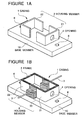
- FIG. 1A there is shown a metal case for a laser diode module for optical communication which is one embodiment of the metal casing in accordance with the present invention.
- the metal case shown in Figure 1A comprises a base member 10 and an enclosure member 2 integrally formed of an alloy including copper, tungsten and nickel.
- the enclosure member 2 is composed of a front member 21 and a rear member 22 separately arranged on the base member 10.
- the front member 21 comprises an opening 4 for an window through which optical signals pass.
- the base member 10 comprises holes 6 for screw fixing before and after the enclosure member 2.
- the metal case is produced in net-shape so that no machinery is necessary.
- Figure 1B shows the metal case of Figure 1A to which some elements and parts are assembled.
- terminals 3 mounted on ceramic members 30 are inserted and hermetically fixed in gaps between the front member 21 and the rear member 22.
- a frame 5 is disposed on an upper edge of the enclosure member 2 which contributes fastening of the ceramic members 30 and a cap (not shown).
- glass 40 is hermetically fitted to the opening 4.
- the metal case is formed of an alloy including copper, nickel and tungsten or an alloy including copper, nickel and molybdenum or an alloy including copper, nickel, tungsten and molybdenum having high thermal conductivity and a thermal expansion coefficient similar to the ceramic and glass.
- the alloy has a content of 20 to 50 percent by volume of copper and equal to or less than 1 percent by weight of nickel and the remainder is tungsten and/or molybdenum. A ratio between tungsten and molybdenum can be arbitrarily selected.
- the copper content of the alloy is less than 20 percent by volume, inner pores are prone to be formed so that the alloy is hard to be packed.
- the alloy having such a composite does not have stable characteristics, in particular its thermal conductivity is unstable so that it is not suitable for the metal case.
- the thermal expansion coefficient of the alloy becomes larger than 10 ⁇ 10 -6 /°C, so that difference in thermal expansion coefficient between the alloy and the ceramic and glass materials becomes too large.
- the nickel of small content of equal to or less than 1 percent by weight give a preferable effect during the process for preparing the metal case so that the characteristics of the metal case is improved. However, if the nickel content of the alloy excesses 1 percent by weight, the thermal conductivity of the alloy becomes lower , which is not preferable.
- the metal case shown in Figure 1A was manufactured by the following process. At first, tungsten powder having an average particle diameter of 3 ⁇ m and nickel powder having an average particle diameter of 4 ⁇ m were admixed with a ratio of 99.9 to 0.1 by weight.
- Molybdenum powder a mixture of tungsten powder and molybdenum powder and a tungsten-molybdenum alloy powder can be used instead of the tungsten powder.
- the average particle diameters of the metal powders are preferably equal to or smaller than 40 ⁇ m. If the average particle diameters are larger than 40 ⁇ m, products will be too brittle.
- the wax preferably have a melting point equal to or lower than 100 °C.
- the organic binder is preferably composed of the wax and an organic material which hardly leaves ash.
- the mixed metal powder of the tungsten powder and nickel powder and the organic binder were mixed with a ratio of 38 to 62 by volume and kneaded.
- the kneaded admixture was injection molded so as to form a green shape of the metal case.
- the ratio between the mixed metal powder and the organic binder are determined so that the green shape will have porosities of 20 to 50 percent by volume after it is debinderized.
- the green shape was debinderized by a two-stage treatment. At first, the green shape was debinderized by vapor of methylene chloride (boiling point : 40°C) for 5 hours. Then, the green shape was debinderized by heating to 800 °C for 30 minutes in hydrogen gas.
- the green shape After the two-stage treatment, the green shape had a good appearance and there was no distortion and warping so that a configuration of each part was maintained. A porosity rate of the green shape was 38 percent by volume.
- an organic binder composed of a wax having a low melting point and a organic material which hardly leaves ash is used.
- the organic material is stable at the melting point of the wax.
- the green shape is debinderized by vapor of an organic solvent, which removes the wax and debinderizes surfaces of the green shape and forms guide porosities.
- the green shape is heated so as to vaporize the organic material so that the green shape is completely debinderized.
- the organic solvent preferably has a boiling point lower than a melting point or a softening point of the organic material to avoid distortion of the green shape during the vaporization of the binder.
- the organic solvent is preferably selected from ethanol, acetone, trichlororthane, carbon tetrachloride, methylene chloride, etc.
- the heat treatment is preferably conducted under an atmosphere which does not include oxygen, for example, hydrogen atmosphere in order to oxidize the green shape.
- the porosity rate of the green shape should be 20 to 50 percent by volume. If it is smaller than 20 percent by volume, a copper content of the products will be lower than 20 percent by volume. If the porosity rate is larger than 50 percent by volume, a copper content of the products will be higher than 50 percent by volume so that thermal expansion coefficients of the products become higher than 10 ⁇ 10 -6 /°C.
- boron nitride powder dispersed in water was sprayed to all the surface of the green shape excluding the back to a thickness of 10 ⁇ m.
- the boron nitride powder prevented effusion of copper in the successive process.
- the powder for preventing copper effusion should be formed of a material or materials which is not wetted by molten copper, is physically and chemically stable at the infiltration so that it does not react with the porous green shape and is easily removed after the infiltration.
- the material of the powder can be one or ones selected from carbides, nitrides and oxides, in particular, Al 2 O 3 , TiO 2 , SiO 2 , ZrO 2 , A1N, BN, Si 3 N 4 , TiN, ZrN, SiC, ZrC and TiC. Powder of another material can not enough prevent the effusion of copper or is hard to remove after the process.
- the green shape was placed on a copper plate having sides equal to the base member and a thickness of 1 mm, so that copper was infiltrated into the green shape in a continuous furnace under hydrogen atmosphere at a temperature of 1150 °C.
- the boron nitride powder prevents effusion of molten copper.
- the boron nitride powder was removed by liquid honing and residual molten copper was removed by plane grinding, so that the metal case in accordance with the present invention was completed.
- the metal case was formed of a specified metal texture composite had tungsten-nickel admixture skeleton and copper infiltration filler. No copper effusion occurred on the surfaces of the metal case on which the effusion preventive boron nitride powder had been applied. After the infiltration, the dimensions of the product contracted at a rate of 0.8 percent.
- Sample Nos. 1 to 10 are present invention using W-Ni powder.
- Sample Nos. 11 to 113 are present invention using Mo-Ni powder.
- Sample Nos. 14 to 16 are comparative examples using W-Ni powder.
- the mold was completely filled with the admixture so that a shape of required density could not be obtained.
- sample 15 the green shape foamed during the debinderization so that a required porous green shape could not be obtained.
- Sample No. 10 had the largest contraction rate of 1.8 percent.
- the contraction occurred during the infiltration and the rate of the contraction was determined by the rate of porosities of the porous green shape. If the rate of porosities of the porous green shape was equal to or less than 30 percent by volume, the contraction hardly occurred. If the rate of porosities of the porous green shape excessed 30 percent by volume, the contraction occurred corresponding to the rate of porosities. However, according to the present invention, the contraction rate was at most 2 percent. In addition, this small contraction had no effect on the characteristics of the alloy and on accuracy of the size.
- the thermal conductivities and the thermal expansion coefficients of the alloys shown in Table 2 are suitable for metal casings for semiconductor devices.
- metal case assemblies shown in Figure 1B were prepared by using the metal cases according to the present invention, and the metal cases of the Comparative example 1 and 2.
- Each of the metal case assemblies was nickel plated to a deposit thickness of 1.5 ⁇ m and further gold plated to a deposit thickness of 1.5 ⁇ m.
- Sapphire members were hermetically soldered to the openings 4 by using gold-tin solder.
- Heat-resistance and gastightness after 100 heat cycles were respectively evaluated for each 200 metal cases.
- the heat-resistance was evaluated by observing surfaces of the metal cases by using a optical microscope at a magnification of ⁇ 20 so as to find blisters, stains and change in color after heating the metal cases to 450 °C for 5 minutes under the air.
- the metal case assembly was disposed on a flange 41 through an O-ling 42 so as to be evacuated. Then, helium gas was jetted to the metal case so that leak rate of the helium gas was measured through the flange by helium detector. Metal cases having a leak rate of higher than 5 ⁇ 10 -8 atm•cm 3 /sec. were determined to be detective products. The results were shown in the following Table 4.
- the metal cases of comparative examples 1 and 2 had larger distortions and warpings than that of the present invention so that optical couplings deviated so as to lower optical power.
- FIG. 2A there is shown a metal header for a laser diode for optical communication which is one embodiment of the metal casing in accordance with the present invention.
- the metal header shown in Figure 2A comprises a base member 10 formed of an alloy including copper, tungsten and nickel.
- the base member 10 comprises holes 8 for terminals and a depression 9 for semiconductor device such as a laser diode.
- Figure 2B shows the metal header of Figure 2A to which some elements and parts are assembled.
- terminals 3 are inserted into the holes 8 and hermetically fixed by sealing glass.
- a semiconductor device 7 is disposed in the depression 9.
- the metal header is formed of an alloy including copper, nickel and tungsten or an alloy including copper, nickel and molybdenum or an alloy including copper, nickel, tungsten and molybdenum having high thermal conductivity and a thermal expansion coefficient similar to the ceramic and glass.
- the alloy has a content of 20 to 50 percent by volume of copper and equal to or less than 1 percent by weight of nickel and the remainder is tungsten and/or molybdenum. A ratio between tungsten and molybdenum can be arbitrarily selected.
- the metal header can be manufactured without costly and troublesome machinery. Namely, a net-shape metal header having the holes and depressions can be obtained.
- FIG. 3A there is shown a metal header for microwave devices which is one embodiment of the metal casing in accordance with the present invention.
- the metal header shown in Figure 3A comprises a base member 10 formed of an alloy including copper, tungsten and nickel.
- the base member 10 comprises holes 8 for terminals and depressions 9 for semiconductor devices such as microwave devices.
- Figure 3B shows the metal header of Figure 3A to which some elements and parts are assembled.
- terminals 3 are inserted into the holes 8 and hermetically fixed by sealing glass.
- Semiconductor devices 7 are disposed in the depressions 9.
- a frame 5 for a sealing cap (not shown) is disposed on an edge of the base member 10.
- the metal header is formed of an alloy including copper, nickel and tungsten or an alloy including copper, nickel and molybdenum or an alloy including copper, nickel, tungsten and molybdenum having high thermal conductivity and a thermal expansion coefficient similar to the ceramic and glass.
- the alloy has a content of 20 to 50 percent by volume of copper and equal to or less than 1 percent by weight of nickel and the remainder is tungsten and/or molybdenum. A ratio between tungsten and molybdenum can be arbitrarily selected.
- the metal header can be manufactured without costly and troublesome machinery. Namely, a net-shape metal header having the holes and depressions can be obtained.
Landscapes
- Physics & Mathematics (AREA)
- Condensed Matter Physics & Semiconductors (AREA)
- General Physics & Mathematics (AREA)
- Electromagnetism (AREA)
- Optics & Photonics (AREA)
- Cooling Or The Like Of Semiconductors Or Solid State Devices (AREA)
- Semiconductor Lasers (AREA)
- Powder Metallurgy (AREA)
Applications Claiming Priority (3)
| Application Number | Priority Date | Filing Date | Title |
|---|---|---|---|
| JP25381893 | 1993-09-16 | ||
| JP25381893 | 1993-09-16 | ||
| EP94402072A EP0645804B1 (de) | 1993-09-16 | 1994-09-16 | Metallgehäuse für Halbleiterbauelement und Verfahren zu seiner Herstellung |
Related Parent Applications (1)
| Application Number | Title | Priority Date | Filing Date |
|---|---|---|---|
| EP94402072A Division EP0645804B1 (de) | 1993-09-16 | 1994-09-16 | Metallgehäuse für Halbleiterbauelement und Verfahren zu seiner Herstellung |
Publications (2)
| Publication Number | Publication Date |
|---|---|
| EP1282166A2 true EP1282166A2 (de) | 2003-02-05 |
| EP1282166A3 EP1282166A3 (de) | 2003-03-05 |
Family
ID=17256568
Family Applications (2)
| Application Number | Title | Priority Date | Filing Date |
|---|---|---|---|
| EP94402072A Expired - Lifetime EP0645804B1 (de) | 1993-09-16 | 1994-09-16 | Metallgehäuse für Halbleiterbauelement und Verfahren zu seiner Herstellung |
| EP02023598A Withdrawn EP1282166A3 (de) | 1993-09-16 | 1994-09-16 | Metallgehäuse für Halbleiterbauelement mit hoher thermischer Leitfähigkeit und gleichem thermischen Ausdehnungskoeffizienten wie der Halbleiter, und Verfahren zu seiner Herstellung |
Family Applications Before (1)
| Application Number | Title | Priority Date | Filing Date |
|---|---|---|---|
| EP94402072A Expired - Lifetime EP0645804B1 (de) | 1993-09-16 | 1994-09-16 | Metallgehäuse für Halbleiterbauelement und Verfahren zu seiner Herstellung |
Country Status (3)
| Country | Link |
|---|---|
| US (1) | US5574959A (de) |
| EP (2) | EP0645804B1 (de) |
| DE (1) | DE69432546T2 (de) |
Cited By (1)
| Publication number | Priority date | Publication date | Assignee | Title |
|---|---|---|---|---|
| WO2008095080A1 (en) * | 2007-01-31 | 2008-08-07 | Arcmelt Company, Lc. | Method of producing composite materials through metal injection molding |
Families Citing this family (17)
| Publication number | Priority date | Publication date | Assignee | Title |
|---|---|---|---|---|
| DE19614006A1 (de) * | 1996-04-09 | 1997-10-16 | Basf Ag | Verfahren zur Herstellung von Granulat und Formteilen aus Hartmetall- oder Cermet-Materialien |
| US5831290A (en) * | 1997-02-25 | 1998-11-03 | Quarton, Inc. | Laser diode mounting structure |
| KR100217032B1 (ko) * | 1997-06-14 | 1999-09-01 | 박호군 | 구리 용침용 텅스텐 골격 구조 제조 방법 및 이를 이용한 텅스텐-구리 복합재료 제조 방법 |
| KR100215547B1 (ko) * | 1997-06-14 | 1999-08-16 | 박원훈 | 마이크로파 소자용 텅스텐-구리 밀폐 패키지용 용기 및 그의 제조 방법 |
| US6319459B1 (en) | 1999-10-18 | 2001-11-20 | Kemet Electronics Corporation | Removal of organic acid based binders from powder metallurgy compacts |
| US6405785B1 (en) | 2000-01-28 | 2002-06-18 | Mold-Masters Limited | Injection molding component with heating element and method of making |
| US6838046B2 (en) * | 2001-05-14 | 2005-01-04 | Honeywell International Inc. | Sintering process and tools for use in metal injection molding of large parts |
| JP2003052185A (ja) * | 2001-05-30 | 2003-02-21 | Canon Inc | 電力変換器およびそれを用いる光起電力素子モジュール並びに発電装置 |
| US6770114B2 (en) | 2001-12-19 | 2004-08-03 | Honeywell International Inc. | Densified sintered powder and method |
| GB2387714A (en) * | 2002-04-19 | 2003-10-22 | Denselight Semiconductors Pte | Mount for a semiconductor device |
| US7063815B2 (en) * | 2003-12-05 | 2006-06-20 | Agency For Science, Technology And Research | Production of composite materials by powder injection molding and infiltration |
| JP2007520635A (ja) * | 2004-02-04 | 2007-07-26 | ジーケーエヌ シンター メタルズ, インコーポレーテッド | 粉末金属部品のシート材料溶浸 |
| US7186369B1 (en) * | 2004-08-04 | 2007-03-06 | The United States Of America As Represented By The Secretary Of The Navy | Method of forming a part made of a molybdenum-copper composite material |
| US7341093B2 (en) * | 2005-02-11 | 2008-03-11 | Llc 2 Holdings Limited, Llc | Copper-based alloys and their use for infiltration of powder metal parts |
| DE102007048617A1 (de) * | 2007-10-10 | 2009-04-16 | Robert Bosch Gmbh | Lasermodul |
| KR101000684B1 (ko) * | 2007-10-11 | 2010-12-10 | 세종대학교산학협력단 | 이산화티타늄 나노튜브분말 및 이를 이용한 고압수소저장탱크 삽입용 판형 필름의 제조방법 |
| FR2985855B1 (fr) * | 2012-01-17 | 2014-11-21 | Soc Fr Detecteurs Infrarouges Sofradir | Procede pour la realisation de traversees electriques etanches au travers d'un boitier d'encapsulation et boitier d'encapsulation muni d'au moins l'une de ces traversees electriques |
Family Cites Families (19)
| Publication number | Priority date | Publication date | Assignee | Title |
|---|---|---|---|---|
| DE2137829B2 (de) * | 1970-08-01 | 1975-11-13 | Institutul De Cercetari Metalurgice Icem, Bukarest | Verfahren zur Herstellung des Werkstoffes für eine Funkenerosions-Elektrode |
| US3929476A (en) * | 1972-05-05 | 1975-12-30 | Minnesota Mining & Mfg | Precision molded refractory articles and method of making |
| US4431449A (en) * | 1977-09-26 | 1984-02-14 | Minnesota Mining And Manufacturing Company | Infiltrated molded articles of spherical non-refractory metal powders |
| GB1603855A (en) * | 1978-05-10 | 1981-12-02 | Johnson Matthey Co Ltd | Resin-impregnated sintered silver articles |
| US4373127A (en) * | 1980-02-06 | 1983-02-08 | Minnesota Mining And Manufacturing Company | EDM Electrodes |
| US4327156A (en) * | 1980-05-12 | 1982-04-27 | Minnesota Mining And Manufacturing Company | Infiltrated powdered metal composite article |
| US4554218A (en) * | 1981-11-05 | 1985-11-19 | Minnesota Mining And Manufacturing Company | Infiltrated powered metal composite article |
| US4491558A (en) * | 1981-11-05 | 1985-01-01 | Minnesota Mining And Manufacturing Company | Austenitic manganese steel-containing composite article |
| JPS6048550B2 (ja) * | 1981-12-31 | 1985-10-28 | 豊信 水谷 | 高温溶融金属用耐蝕性塗料 |
| JPS5921032A (ja) * | 1982-07-26 | 1984-02-02 | Sumitomo Electric Ind Ltd | 半導体装置用基板 |
| JPS59143347A (ja) * | 1983-02-03 | 1984-08-16 | Sumitomo Electric Ind Ltd | 半導体基板材料の製造方法 |
| US4710223A (en) * | 1986-03-21 | 1987-12-01 | Rockwell International Corporation | Infiltrated sintered articles |
| US5017526A (en) * | 1986-05-08 | 1991-05-21 | Lanxide Technology Company, Lp | Methods of making shaped ceramic composites |
| DE3881030T2 (de) * | 1987-09-28 | 1993-12-02 | Witec Cayman Patents Ltd | Kupfer-wolfram-metallmischung sowie verfahren. |
| DE68913800T2 (de) * | 1988-04-30 | 1994-07-14 | Toyota Motor Co Ltd | Verfahren zur Herstellung von Verbundmetall unter Beschleunigung der Infiltration des Matrix-Metalls durch feine Teilchen eines dritten Materials. |
| IT1230629B (it) * | 1988-11-11 | 1991-10-28 | Nuova Samin Spa | Procedimento per la produzione di materiali compositi a matrice metallica a contenuto di rinforzo controllato |
| JP2746279B2 (ja) * | 1990-06-18 | 1998-05-06 | 日本タングステン 株式会社 | 半導体装置用基板材料及びその製造方法 |
| US5342573A (en) * | 1991-04-23 | 1994-08-30 | Sumitomo Electric Industries, Ltd. | Method of producing a tungsten heavy alloy product |
| JPH05222402A (ja) * | 1992-02-12 | 1993-08-31 | Sumitomo Electric Ind Ltd | タングステン重合金製品の製造方法 |
-
1994
- 1994-09-16 DE DE69432546T patent/DE69432546T2/de not_active Expired - Lifetime
- 1994-09-16 EP EP94402072A patent/EP0645804B1/de not_active Expired - Lifetime
- 1994-09-16 US US08/306,955 patent/US5574959A/en not_active Expired - Lifetime
- 1994-09-16 EP EP02023598A patent/EP1282166A3/de not_active Withdrawn
Cited By (1)
| Publication number | Priority date | Publication date | Assignee | Title |
|---|---|---|---|---|
| WO2008095080A1 (en) * | 2007-01-31 | 2008-08-07 | Arcmelt Company, Lc. | Method of producing composite materials through metal injection molding |
Also Published As
| Publication number | Publication date |
|---|---|
| EP0645804A3 (de) | 1996-05-29 |
| EP1282166A3 (de) | 2003-03-05 |
| EP0645804A2 (de) | 1995-03-29 |
| DE69432546D1 (de) | 2003-05-28 |
| US5574959A (en) | 1996-11-12 |
| EP0645804B1 (de) | 2003-04-23 |
| DE69432546T2 (de) | 2003-11-20 |
Similar Documents
| Publication | Publication Date | Title |
|---|---|---|
| EP0645804B1 (de) | Metallgehäuse für Halbleiterbauelement und Verfahren zu seiner Herstellung | |
| JP3841633B2 (ja) | 半導体レーザモジュール | |
| EP0100232B2 (de) | Substrat für Halbleiterapparat | |
| US5770821A (en) | Submount | |
| US6270848B1 (en) | Heat sink material for use with semiconductor component and method for fabricating the same, and semiconductor package using the same | |
| EP0521405A1 (de) | Wärmeabführendes Bauteil und damit versehene Halbleitervorrichtung | |
| EP0297511A2 (de) | Verbindungsstruktur zwischen Bauelementen für Halbleiterapparat | |
| US4704320A (en) | Substrate structure | |
| KR102368742B1 (ko) | 유지 장치 및 유지 장치의 제조 방법 | |
| US5998733A (en) | Graphite aluminum metal matrix composite microelectronic package | |
| KR101432320B1 (ko) | 접합 구조체 및 그 제조 방법 | |
| KR20010079642A (ko) | 복합 재료 및 그를 이용한 반도체 장치 | |
| US7518205B2 (en) | Semiconductor package and method for manufacturing the same | |
| EP0482812B1 (de) | Verfahren zum Herstellen von wärmestrahlender Substraten zum Montieren von Halbleitern und gemäss diesem Verfahren hergestellte Halbleiterpackung | |
| KR100459748B1 (ko) | 정전기 척 및 이의 제조방법 | |
| EP0113088B1 (de) | Trägersubstrat für Halbleiterelement | |
| KR100413848B1 (ko) | 광모듈용 밀폐형 패키지 | |
| JP2523162B2 (ja) | 半導体装置用部材 | |
| JP3561975B2 (ja) | 半導体装置用金属部品の製造方法 | |
| US20010024725A1 (en) | Package and method of manufacturing the same | |
| US5132779A (en) | Housing for semiconductor device with occlusion gas removed | |
| JP3945375B2 (ja) | 光半導体モジュール用パッケージ | |
| JPH09205174A (ja) | 気密端子基板とその製造方法 | |
| JP2650044B2 (ja) | 半導体装置用部品間の接続構造 | |
| US20030001259A1 (en) | Hermetically sealing enclosure for housing photo-semiconductor devices and photo-semiconductor module incorporating the enclosure |
Legal Events
| Date | Code | Title | Description |
|---|---|---|---|
| PUAI | Public reference made under article 153(3) epc to a published international application that has entered the european phase |
Free format text: ORIGINAL CODE: 0009012 |
|
| PUAL | Search report despatched |
Free format text: ORIGINAL CODE: 0009013 |
|
| AC | Divisional application: reference to earlier application |
Ref document number: 0645804 Country of ref document: EP Kind code of ref document: P |
|
| AK | Designated contracting states |
Designated state(s): DE FR GB IT NL SE |
|
| AK | Designated contracting states |
Kind code of ref document: A3 Designated state(s): DE FR GB IT NL SE Designated state(s): DE FR GB IT NL SE |
|
| 17P | Request for examination filed |
Effective date: 20030905 |
|
| AKX | Designation fees paid |
Designated state(s): DE FR GB IT NL SE |
|
| 17Q | First examination report despatched |
Effective date: 20100726 |
|
| GRAP | Despatch of communication of intention to grant a patent |
Free format text: ORIGINAL CODE: EPIDOSNIGR1 |
|
| STAA | Information on the status of an ep patent application or granted ep patent |
Free format text: STATUS: THE APPLICATION IS DEEMED TO BE WITHDRAWN |
|
| 18D | Application deemed to be withdrawn |
Effective date: 20130403 |