EP1280271A2 - Vorwärtsgekoppelter Verstärkervorrichtung und Verfahren - Google Patents
Vorwärtsgekoppelter Verstärkervorrichtung und Verfahren Download PDFInfo
- Publication number
- EP1280271A2 EP1280271A2 EP02016215A EP02016215A EP1280271A2 EP 1280271 A2 EP1280271 A2 EP 1280271A2 EP 02016215 A EP02016215 A EP 02016215A EP 02016215 A EP02016215 A EP 02016215A EP 1280271 A2 EP1280271 A2 EP 1280271A2
- Authority
- EP
- European Patent Office
- Prior art keywords
- output
- coupler
- amplifier
- signal
- circuit
- Prior art date
- Legal status (The legal status is an assumption and is not a legal conclusion. Google has not performed a legal analysis and makes no representation as to the accuracy of the status listed.)
- Granted
Links
Images


Classifications
-
- H—ELECTRICITY
- H03—ELECTRONIC CIRCUITRY
- H03F—AMPLIFIERS
- H03F1/00—Details of amplifiers with only discharge tubes, only semiconductor devices or only unspecified devices as amplifying elements
- H03F1/32—Modifications of amplifiers to reduce non-linear distortion
- H03F1/3223—Modifications of amplifiers to reduce non-linear distortion using feed-forward
- H03F1/3229—Modifications of amplifiers to reduce non-linear distortion using feed-forward using a loop for error extraction and another loop for error subtraction
- H03F1/3235—Modifications of amplifiers to reduce non-linear distortion using feed-forward using a loop for error extraction and another loop for error subtraction using a pilot signal
-
- H—ELECTRICITY
- H03—ELECTRONIC CIRCUITRY
- H03F—AMPLIFIERS
- H03F2201/00—Indexing scheme relating to details of amplifiers with only discharge tubes, only semiconductor devices or only unspecified devices as amplifying elements covered by H03F1/00
- H03F2201/32—Indexing scheme relating to modifications of amplifiers to reduce non-linear distortion
- H03F2201/3212—Using a control circuit to adjust amplitude and phase of a signal in a signal path
Definitions
- the present invention relates to a feedforward amplifier and a feedforward amplification method used for mobile communication base station equipment and so on.
- a power amplifier of high efficiency and high linearity is required for a transmitter of a mobile communication base station in order to amplify a large number of signaling channels by one operation, and improvement in the linearity is implemented by performing distortion compensation by a feedforward method.
- a feedforward amplifier will not be described in detail here since it is also described in John L. B. Walker, "High-Power GaAs FET Amplifiers," Artech House, 1993, pp. 332 to 333 and so on, for instance.
- CDMA Code Division Multiple Access
- the base station requires switching of output power such as high-speed power control and burst transmission, and high-speed distortion compensation control is also required for feedforward distortion compensation.
- the CDMA method will not be described in detail here since it is also described in Tero Ojanpera et al., "Wideband CDMA For Third Generation Mobile Communications," Artech House, 1998, pp. 58 to 62 and so on, for instance.
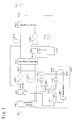
- FIG. 5 is a block diagram thereof (for instance, a feedforward nonlinear distortion compensation amplifier described in Japanese Patent Laid-Open No. 2000-196366).
- reference character IN represents an input terminal
- Zo represents a terminating resistor
- HYB1 represents a first hybrid
- ATT1 represents a first variable attenuator
- PS1 represents a first variable phase shifter
- A1 represents a main amplifier
- D1 represents a first delay element
- HYB2 represents a second hybrid
- D2 represents a second delay element
- ATT2 represents a second variable attenuator
- PS2 represents a second variable phase shifter
- A2 represents an error amplifier
- HYB3 represents a third hybrid
- DC3 represents a first coupler
- DC2 represents a second coupler
- DC4 represents a third coupler
- DC9 represents a fourth coupler
- D3 represents a third delay element
- D4 represents a fourth delay element
- BPF3 represents a band pass filter
- OSC2 represents a local oscillator
- reference numeral 28 denotes an in-phase divider
- 36 denotes a first synchronous detector
- 38 denote
- a pilot signal generated by the local oscillator OSC2 is divided by the in-phase power divider 28, and one of the divided pilot signal is injected from the first coupler DC3 to the main amplifier A1.
- a suppressed signal of a distortion cancellation loop is taken out of the third coupler DC4 and is added to the second synchronous detector 38 together with the other output of the in-phase divider 28 via the band pass filter BPF3 so as to acquire an amplitude error and a phase error.
- the errors thus acquired are added to a control terminal of the second variable attenuator ATT2 and that of the second variable phase shifter PS2 so as to exert control.
- a transmitting carrier taken out of the fourth coupler DC9 as a combined output is added to the synchronous detector 36 via the third delay element D3 and the auto level control circuit 40, and the blocked signal of a distortion detection loop taken out of the second coupler DC2 as a combined output is added to the synchronous detector 36 via the fourth delay element D4.
- the amplitude error and the phase error are outputted therefrom, and the outputted errors are added to the control terminal of the first variable attenuator ATT1 and that of the first variable phase shifter PS1 so as to exert control.
- the auto level control circuit 40 was essential in order to cope with the cases where an output level is significantly changed by a method of a wide dynamic range.
- an accuracy of distortion compensation is apt to be influenced by a temperature change and so on, and so it may be difficult to obtain stable distortion compensation.
- An object of the present invention is, in consideration of the above problems in the past, to provide the feedforward amplifier and the feedforward amplification method capable of performing high-speed distortion compensation control without using the auto level control circuit.
- the 1st invention of the present invention is a feedforward amplifier comprising:
- the 2nd invention of the present invention is the feedforward amplifier according to 1st invention, wherein said in-phase power dividing circuit is connected to the output of said first log amplifier and said 90-degree power dividing circuit is connected to the output of said second log amplifier .
- the 3rd invention of the present invention a feedforward amplifier comprising:
- the 4th invention of the present invention is the feedforward amplifier according to 3rd invention, wherein said in-phase power dividing circuit is connected to the output of said first log amplifier and said 90-degree power dividing circuit is connected to the output of said second log amplifier; said first mixer is connected to one of the outputs of said in-phase power dividing circuit and one of the outputs of said 90-degree power dividing circuit; said second mixer is connected to the other output of said in-phase power dividing circuit and the other output of said 90-degree power dividing circuit; and said third and fourth log amplifiers are omitted.
- the 5th invention of the present invention is the feedforward amplifier according to any of 1st to 4th inventions, wherein said fifth coupler is inserted between the output of said first delay element and said second coupler or between the output of said first coupler and the input of said first delay element.
- the 6th invention of the present invention is the feedforward amplifieraccording to any of 1st to 4th inventions , wherein said fifth coupler is inserted at the inputs of said main amplifier or between the stages of said main amplifier.
- the 7th invention of the present invention is the feedforward amplifier according to any of 1st to 4th inventions , wherein said fifth coupler is inserted (1) between the output of said second coupler and the input of said second delay element, (2) between the stages of said second delay element, or (3) between the output of said second delay element and the input of said third coupler.
- the 8th invention of the present invention is the feedforward amplifier according to any of 1st to 4th inventions , wherein said fifth coupler is inserted behind the output of said third coupler or between the combined output of said seventh coupler and the input of said distortion cancellation loop control circuit.
- the 9th invention of the present invention is the feedforward amplifier according to 1st invention, wherein at least one of the amplifier or attenuator is inserted between the second output of said second coupler and the input of said sixth coupler.
- the 10th invention of the present invention is the feedforward amplifier according to 3rd or 4th inventions, wherein said first to fourth log amplifiers are limiter amplifiers.
- the 11th invention of the present invention is the feedforward amplifier according to 3rd or 4th inventions, wherein at least two of said first to fourth log amplifiers, said first and second mixers, said subtraction circuit, said comparator, said inversion circuit, said switching circuit, said in-phase power dividing circuit and said 90-degree power dividing circuit are integrated in the same semiconductor substrate.
- the 12th invention of the present invention is the feedforward amplifier according to 1st invention, comprising:
- the 13th invention of the present invention is the feedforward amplifier according to 12th invention, wherein the output of said power detection circuit is utilized as an output power monitor.
- the 14th invention of the present invention is a feedforward amplifier comprising:
- the 15th invention of the present invention is the feedforward amplifier according to 14th invention, having delaying means of delaying said other output signal, wherein said log amplifier is utilized to control said adjusting means by (1) detecting a phase error as a deviation from an opposite phase of a difference between the phase of said delayed other output signal and the phase of said generated amplification signal, and (2) detecting an amplitude error as a deviation between the amplitude of said delayed other output signal and the amplitude of said generated amplification signal, so that said detected phase error and said detected amplitude error become zero.
- the 16th invention of the present invention is a feedforward amplifying method comprising:
- reference character IN represents an input terminal
- CPL1 represents a first coupler
- VAP1 represents a first vector adjuster
- AMP1 represents a main amplifier
- DLY1 represents a first delay element
- CPL2 represents a second coupler
- DLY2 represents a second delay element
- VAP2 represents a second vector adjuster
- AMP2 represents an error amplifier
- CPL3 represents a third coupler
- CPL4 represents a fourth coupler
- CPL5 represents a fifth coupler
- CPL6 represents a sixth coupler
- CPL7 represents a seventh coupler
- SPL1 represents an in-phase power divider (in-phase power dividing circuit)
- HYB1 represents a 90-degree power divider(90-degree power dividing circuit)
- LOG1 represents a first log amplifier
- LOG2 represents a second log amplifier
- MIX1 represents a first mixer
- MIX2 represents a second mixer
- DIF1 represents a subtraction circuit
- INV1 represents
- CPL1 corresponds to input carrier signal dividing means of the present invention
- VAP1 corresponds to adjusting means of the present invention
- AMP1 corresponds to amplifying means of the present invention
- CPL2 corresponds to distortion signal extractingmeans of the present invention
- CPL3 corresponds to output signal generating means of the present invention
- CNT1 corresponds to control means of the present invention.
- DLY1 corresponds to delaying means of the present invention.
- the distortion cancellation loop control circuit CNT2 inputs and divides a pilot signal outputted from the local oscillator OSC1 which is a local oscillator of generating the pilot signals, and injects the remaining divided pilot signal into an input of the main amplifier AMP1, and then takes the pilot signal suppressed by a distortion cancellation loop out of the seventh coupler CPL7 and inputs it.
- a distortion cancellation loop control circuit CNT2 outputs an amplitude error and a phase error of the error amplifier AMP2 and the second delay element DLY2 from a difference in characteristics of the two pilot signals, and feeds back these errors to the second vector adjuster VAP2 and exerts control so as to maintain a distortion suppressing characteristic of the distortion cancellation loop.
- the distortion detection loop control circuit CNT1 uses a transmitting carrier taken out of the fifth coupler CPL5 (mainly a carrier signal amplified by the main amplifier AMP1) and a transmitting carrier suppressed by a distortion detection loop taken out of the sixth coupler CPL6 (mainly a distortion signal generated when performing amplification by the main amplifier AMP1).
- the transmitting carrier taken out of the fifth coupler CPL5 is divided in the same phase by the in-phase power divider SPL1.
- the suppressed transmitting carrier taken out of the sixth coupler CPL6 is divided with a phase difference of 90 degrees by the 90-degree power divider HYB1.
- One of the outputs of the in-phase power divider SPL1 is amplified by the first log amplifier LOG1, and one of the outputs of the 90-degree power divider HYB1 is amplified by the second log amplifier LOG2, and then the respective outputs are inputted to the first mixer MIX1 so as to obtain a phase error output.
- VA1 is an amplification vector to be taken out of CPL5 (refer to Figure 1) after passing on the amplifier AMP1 (refer to Figure 1) side of the distortion detection loop
- VR1 is a reference signal vector to be combined with VA1 on CPL2 (refer to Figure 1) after passing on the delay element DLY1 (refer to Figure 1) side of the distortion detection loop
- VE1 is an error vector to be taken out of CPL6 (refer to Figure 1) as a sum of the amplification vector VA1 and the reference signal vector VR1.
- the amplification vector VA1 perfectly matches with a vector VA0 (refer to Figure 2) having the same size as the reference signal vector VR1 and a phase difference of 180 degrees. It is because the error vector VE1 is suppressed to perfectly become zero in such a case.
- the error vector VE1 is represented as follows by using the reference signal vector VR1 and the amplification vector VA1.
- VE1 VA1 + VR1
- the reference signal vector VR1 is represented as follows by using a normal vector VA1' of the amplification vector VA1.
- VR1 (-k ⁇ cos ⁇ ) VA1 + (k ⁇ sin ⁇ ) VA1'
- [Equation 1] can be transformed as follows.
- [Equation 3] VE1 (1-k ⁇ cos ⁇ ) VA1 + (k ⁇ sin ⁇ ) VA1'
- the feedforward amplifier has the amplification vector VA1 which is the output of the first log amplifier LOG1 (refer to Figure 1) and the error vector VE1 which is the output of the second log amplifier LOG2 (refer to Figure 1) inputted to the mixer MIX1 (refer to Figure 1), so that the normal vector VA1' of the amplification vector VA1 and the error vector VE1 are synchronously mixed.
- the output of the mixer MIX1 is a phase error voltage output proportional to ⁇ (in short, it is a phase error ERP) which appears as a coefficient of a second term of the [Equation 6].
- the output of the subtraction circuit DIF1 (refer to Figure 1) is an amplitude error voltage proportional to the following. [Equation 7] log ⁇ (1-k) 2 + ( ⁇ ) 2 ⁇
- this embodiment uses the log amplifier to expand a working range of the mixer so as to allow distortion detection loop control to be performed at high speed via no logical circuit and without using the auto level control circuit including unstableness such as the temperature characteristic.
- this embodiment has the in-phase power divider SPL1 and the 90-degree power divider HYB1 placed before the log amplifier, the same effect can be obtained by placing the in-phase divider and the 90-degree power divider on the output side of the log amplifier.
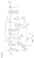
- the feedforward amplifier of Embodiment 2 has the same configuration as the aforementioned feedforward amplifier of Embodiment 1, where the portions in Figure 1 duplicated in Figure. 3 mutually have the same signs and description thereof will be omitted. Moreover, LOG3 is a third log amplifier and LOG4 is a fourth log amplifier.
- the feedforward amplifier of Embodiment 2 requires two log amplifiers of the third and fourth log amplifiers LOG3 and LOG4 as extra compared to the aforementioned feedforward amplifier of Embodiment 1, it does not require a switch such as SW1 (refer to Figure 1) and control thereof is a little easier.
- the distortion detection loop control CNT1 uses the transmitting carrier taken out of the fifth coupler CPL5 and the transmitting carrier suppressed by a distortion detection loop taken out of the sixth coupler CPL6.
- the transmitting carrier taken out of the fifth coupler CPL5 is divided in the same phase by the in-phase power divider SPL1.
- the suppressed transmitting carrier taken out of the sixth coupler CPL6 is divided with a phase difference of 90 degrees by the 90-degree power divider HYB1.
- one of the outputs of the in-phase power divider SPL1 is amplified by the first log amplifier LOG1, and one of the outputs of the 90-degree power divider HYB1 is amplified by the second log amplifier LOG2, and then the respective outputs are inputted to the first mixer MIX1 so as to obtain a phase error output.
- the other output of the in-phase power divider SPL1 is amplified by the third log amplifier LOG3, and the other output of the 90-degree power divider HYB1 is amplified by the fourth log amplifier LOG4, and then the respective outputs are inputted to the second mixer so as to obtain the output proportional to 1-k of the first term of [Equation 6] and obtain the amplitude error output.
- this embodiment uses the log amplifier and expands a working range of the mixer so as to allow distortion detection loop control to be performed at high speed via no logical circuit and without using an auto level control circuit which includes unstableness such as a temperature characteristic.
- this embodiment has the in-phase power divider SPL1 and the 90-degree power divider HYB1 placed on the input of the log amplifier.
- the same effect can be obtained, not only thereby, but by placing the in-phase power divider SPL1 and the 90-degree power divider HYB1 on the output of the log amplifier to share the first and third log amplifiers and share the second and fourth log amplifiers, and besides, the apparatus can thereby be rendered smaller since two log amplifiers can be reduced altogether.
- Embodiments 1 and 2 have the fifth coupler CPL5 placed between the output of the main amplifier AMP1 and the input of the second coupler CPL2.
- the fifth coupler can be placed anywhere as far as the signal to be taken out includes the transmitting carrier which is a reference.
- the same effect can be obtained obviously by placing the fifth coupler CPL5 to take out the transmitting carrier from the following.
- Embodiments 1 and 2 have the sixth coupler CPL6 placed between the output of the second coupler CPL2 and the input of the second vector adjuster via no other element.
- it is not limited to this, but the following are also feasible. (1) To insert the amplifier between the output of the second coupler CPL2 and the input of the sixth coupler CPL6 in order to increase the combined output level of the sixth coupler CPL6, (2) to insert an attenuator or both the attenuator and amplifier between the output of the second coupler CPL2 and the input of the sixth coupler CPL6 in order to curb reflected power from the sixth coupler CPL6 to the second coupler CPL2 and prevent a standing wave.
- the same effect can be obtained by integrating in the same semiconductor substrate at least two of circuit elements constituting the distortion detection loop control circuit CNT1 shown in Embodiments 1 and 2 to render them as an IC, and besides, the apparatus can thereby be rendered smaller.
- the feedforward amplifier of this embodiment 3 has the same configuration as the aforementioned feedforward amplifiers of Embodiments 1 and 2, where the portions in Figure 1 or Figure 3 duplicated in Figure 4 mutually have the same signs and description thereof will be omitted.
- reference character CPL8 represents an eighth coupler
- DET1 represents a power detection circuit
- CMP2 represents a second comparator
- REF1 represents a first reference voltage generation circuit
- REF2 represents a second reference voltage generation circuit
- SW2 represents a second switching circuit
- SW3 represents a third switching circuit.
- the distortion detection loop control circuit CNT1 is the circuit described in Embodiments 1 and 2.
- the power of the transmitting carrier combined and taken out of the eighth coupler CPL8 is detected by the power detection circuit DET1, and a fixed phase control voltage is generated on the first reference voltage generation circuit REF1 and a fixed amplitude control voltage is generated on the second reference voltage generation circuit REF2.
- an adaptive control voltage generated on the distortion detection loop control circuit CNT1 is switched to the fixed phase control voltage or amplitude control voltage on the second and third switching circuits SW2 and SW3 via the second comparator CMP2 according to the size of a detection voltage detected on the power detection circuit DET1.
- the present invention is the feedforward amplifier comprising: input carrier signal dividing means (CPL1) of dividing an input carrier signal into two output signals; adjusting means (VAP1) of adjusting one of the two divided output signals ; amplifying means (AMP1) of amplifying the adjusted one of the output signals to generate an amplification signal; distortion signal extracting means (CPL2) of extracting a distortion signal by utilizing the other output signal of the two divided output signals and the generated amplification signal; output signal generating means (CPL3) of generating the output carrier signal by utilizing the generated amplification signal and the extracted distortion signal; and control means (CNT1) having at least one log amplifier of controlling the adjusting means based on the other output signal and the generated amplification signal.
- DLY1 delaying means of delaying the other output signal
- the log amplifier is utilized to control the adjusting means by (1) detecting the phase error as a deviation from an opposite phase of a difference between the phase of the delayed other output signal and the phase of the generated amplification signal, and (2) detecting the amplitude error as a deviation between the amplitude of the delayed other output signal and the amplitude of the generated amplification signal, so that the detected phase error and the detected amplitude error become zero.
- the phase error voltage is acquired by mixing the carrier signal amplified by the log amplifier, an absolute value of the amplitude error voltage is acquired by a subtractor, and the signal of which phase is displaced by 90 degrees is mixed to determine the sign of the amplitude error and switch it by adapting the sign of the amplitude error voltage, so that it is possible to perform high-speed distortion compensation control without using the auto level control circuit which is unstable due to the temperature characteristic and so on.
- the present invention has an advantage that the high-speed distortion compensation control can be performed without using the auto level control circuit.
Landscapes
- Physics & Mathematics (AREA)
- Nonlinear Science (AREA)
- Engineering & Computer Science (AREA)
- Power Engineering (AREA)
- Amplifiers (AREA)
Applications Claiming Priority (2)
| Application Number | Priority Date | Filing Date | Title |
|---|---|---|---|
| JP2001218419 | 2001-07-18 | ||
| JP2001218419 | 2001-07-18 |
Publications (3)
| Publication Number | Publication Date |
|---|---|
| EP1280271A2 true EP1280271A2 (de) | 2003-01-29 |
| EP1280271A3 EP1280271A3 (de) | 2006-11-22 |
| EP1280271B1 EP1280271B1 (de) | 2011-06-29 |
Family
ID=19052598
Family Applications (1)
| Application Number | Title | Priority Date | Filing Date |
|---|---|---|---|
| EP02016215A Expired - Lifetime EP1280271B1 (de) | 2001-07-18 | 2002-07-18 | Vorwärtsgekoppelter Verstärkervorrichtung und Verfahren |
Country Status (3)
| Country | Link |
|---|---|
| US (1) | US6791409B2 (de) |
| EP (1) | EP1280271B1 (de) |
| CN (1) | CN1241324C (de) |
Families Citing this family (5)
| Publication number | Priority date | Publication date | Assignee | Title |
|---|---|---|---|---|
| US6850115B2 (en) * | 2002-08-26 | 2005-02-01 | Powerwave Technologies, Inc. | Enhanced efficiency LDMOS based feed forward amplifier |
| CN100539399C (zh) * | 2004-03-11 | 2009-09-09 | 电力波技术公司 | 用于控制自适应前馈放大器中的回路对准的系统和方法 |
| US8594591B2 (en) * | 2009-12-17 | 2013-11-26 | Mitsubishi Electric Corporation | Transmission system |
| CN103873005B (zh) * | 2012-12-10 | 2017-10-24 | 北京普源精电科技有限公司 | 射频信号源及其工作方法 |
| CN104868487B (zh) * | 2015-05-07 | 2017-08-29 | 国家电网公司 | 低频段抑制加强型抗反调电力系统稳定方法 |
Citations (2)
| Publication number | Priority date | Publication date | Assignee | Title |
|---|---|---|---|---|
| EP0996225A1 (de) | 1998-10-22 | 2000-04-26 | Japan Radio Co., Ltd | Verstärker mit Vorwärtskopplungskreisen zur Beseitigung von nichtlinearen Vorverzerrungen |
| EP1001525A1 (de) | 1998-11-13 | 2000-05-17 | Powerwave Technologies, Inc. | Vorwärtsgekoppelte Kompensation mit Phasen- und Zeitmodulation |
Family Cites Families (4)
| Publication number | Priority date | Publication date | Assignee | Title |
|---|---|---|---|---|
| US4580105A (en) * | 1985-01-25 | 1986-04-01 | At&T Bell Laboratories | Automatic reduction of intermodulation products in high power linear amplifiers |
| US6052023A (en) * | 1998-08-31 | 2000-04-18 | Lucent Technologies Inc. | Calibration system for feed forward distortion reduction system |
| JP2000252758A (ja) * | 1999-03-01 | 2000-09-14 | Fujitsu Ltd | 位相補正増幅器及び該位相補正増幅器を用いたフィード・フォワード増幅器 |
| JP3533351B2 (ja) * | 1999-12-28 | 2004-05-31 | 日本無線株式会社 | フィードフォワード増幅器及びその制御回路 |
-
2002
- 2002-07-17 CN CNB021268878A patent/CN1241324C/zh not_active Expired - Fee Related
- 2002-07-18 US US10/198,251 patent/US6791409B2/en not_active Expired - Lifetime
- 2002-07-18 EP EP02016215A patent/EP1280271B1/de not_active Expired - Lifetime
Patent Citations (3)
| Publication number | Priority date | Publication date | Assignee | Title |
|---|---|---|---|---|
| EP0996225A1 (de) | 1998-10-22 | 2000-04-26 | Japan Radio Co., Ltd | Verstärker mit Vorwärtskopplungskreisen zur Beseitigung von nichtlinearen Vorverzerrungen |
| JP2000196366A (ja) | 1998-10-22 | 2000-07-14 | Japan Radio Co Ltd | フィ―ドフォワ―ド非線形歪補償増幅器 |
| EP1001525A1 (de) | 1998-11-13 | 2000-05-17 | Powerwave Technologies, Inc. | Vorwärtsgekoppelte Kompensation mit Phasen- und Zeitmodulation |
Non-Patent Citations (1)
| Title |
|---|
| TERO OJANPERA ET AL.: "Wideband CDMA For Third Generation Mobile Communications", ARTECH HOUSE, 1998, pages 58 - 62 |
Also Published As
| Publication number | Publication date |
|---|---|
| CN1241324C (zh) | 2006-02-08 |
| US20030020541A1 (en) | 2003-01-30 |
| EP1280271A3 (de) | 2006-11-22 |
| EP1280271B1 (de) | 2011-06-29 |
| CN1398131A (zh) | 2003-02-19 |
| US6791409B2 (en) | 2004-09-14 |
Similar Documents
| Publication | Publication Date | Title |
|---|---|---|
| US6242979B1 (en) | Linearization using parallel cancellation in linear power amplifier | |
| US6646505B2 (en) | Power amplifier array with same type predistortion amplifier | |
| KR100438445B1 (ko) | 비선형 왜곡 보상 방법 및 비선형 왜곡 보상 회로 | |
| KR20010056500A (ko) | 전력증폭기의 왜곡 성분 검출장치 | |
| US6211734B1 (en) | Active distortion signal generating circuit for a line-distortion type power amplifier | |
| KR100296146B1 (ko) | 소신호선형화장치 | |
| EP1193861B1 (de) | Vorwärtskopplungsverstärker | |
| JPH03198511A (ja) | 低歪高周波増幅装置 | |
| CA2288460C (en) | Distortion compensation circuit | |
| US6744314B2 (en) | Wideband power amplifier linearization technique | |
| EP1280271A2 (de) | Vorwärtsgekoppelter Verstärkervorrichtung und Verfahren | |
| US5955917A (en) | Nonlinear amplifier calibration system and methods | |
| US6037837A (en) | Feed forward amplifier | |
| US6904267B2 (en) | Amplifying device | |
| US6720829B2 (en) | Distortion-compensated amplifying circuit | |
| EP1289128B1 (de) | Vorwärtsgekoppelter Verstärker und Verfahren zum vorwärtsgekoppelten Verstärken | |
| EP1289129A1 (de) | Verstärker mit Vorverzerrung | |
| JP3911452B2 (ja) | フィードフォワード増幅器 | |
| EP1353438B1 (de) | Vorwärtskopplungsverstärker, kommunikationsvorrichtung, vorwärtskopplungsverstärkungsverfahren, programm und medium | |
| KR100313919B1 (ko) | 이득및위상보상기능을갖는선왜곡전력증폭기 | |
| KR100371531B1 (ko) | 에러 피드백을 이용한 피드포워드 선형 전력 증폭기 | |
| US6657490B2 (en) | Feedforward signal generation for combined amplifiers | |
| JP3358240B2 (ja) | フィードフォワード増幅器 | |
| JPH07101819B2 (ja) | 多周波同時増幅器における歪補償回路 | |
| KR20010028084A (ko) | 전력증폭기의 전치보상기 |
Legal Events
| Date | Code | Title | Description |
|---|---|---|---|
| PUAI | Public reference made under article 153(3) epc to a published international application that has entered the european phase |
Free format text: ORIGINAL CODE: 0009012 |
|
| AK | Designated contracting states |
Designated state(s): AT BE BG CH CY CZ DE DK EE ES FI FR GB GR IE IT LI LU MC NL PT SE SK TR |
|
| AX | Request for extension of the european patent |
Extension state: AL LT LV MK RO SI |
|
| PUAL | Search report despatched |
Free format text: ORIGINAL CODE: 0009013 |
|
| AK | Designated contracting states |
Kind code of ref document: A3 Designated state(s): AT BE BG CH CY CZ DE DK EE ES FI FR GB GR IE IT LI LU MC NL PT SE SK TR |
|
| AX | Request for extension of the european patent |
Extension state: AL LT LV MK RO SI |
|
| 17P | Request for examination filed |
Effective date: 20070302 |
|
| AKX | Designation fees paid |
Designated state(s): DE GB |
|
| RAP1 | Party data changed (applicant data changed or rights of an application transferred) |
Owner name: PANASONIC CORPORATION |
|
| 17Q | First examination report despatched |
Effective date: 20100204 |
|
| GRAP | Despatch of communication of intention to grant a patent |
Free format text: ORIGINAL CODE: EPIDOSNIGR1 |
|
| GRAS | Grant fee paid |
Free format text: ORIGINAL CODE: EPIDOSNIGR3 |
|
| GRAA | (expected) grant |
Free format text: ORIGINAL CODE: 0009210 |
|
| AK | Designated contracting states |
Kind code of ref document: B1 Designated state(s): DE GB |
|
| REG | Reference to a national code |
Ref country code: GB Ref legal event code: FG4D |
|
| REG | Reference to a national code |
Ref country code: DE Ref legal event code: R096 Ref document number: 60240378 Country of ref document: DE Effective date: 20110818 |
|
| PGFP | Annual fee paid to national office [announced via postgrant information from national office to epo] |
Ref country code: DE Payment date: 20110914 Year of fee payment: 10 Ref country code: GB Payment date: 20110719 Year of fee payment: 10 |
|
| PLBE | No opposition filed within time limit |
Free format text: ORIGINAL CODE: 0009261 |
|
| STAA | Information on the status of an ep patent application or granted ep patent |
Free format text: STATUS: NO OPPOSITION FILED WITHIN TIME LIMIT |
|
| 26N | No opposition filed |
Effective date: 20120330 |
|
| REG | Reference to a national code |
Ref country code: DE Ref legal event code: R097 Ref document number: 60240378 Country of ref document: DE Effective date: 20120330 |
|
| GBPC | Gb: european patent ceased through non-payment of renewal fee |
Effective date: 20120718 |
|
| PG25 | Lapsed in a contracting state [announced via postgrant information from national office to epo] |
Ref country code: DE Free format text: LAPSE BECAUSE OF NON-PAYMENT OF DUE FEES Effective date: 20130201 Ref country code: GB Free format text: LAPSE BECAUSE OF NON-PAYMENT OF DUE FEES Effective date: 20120718 |
|
| REG | Reference to a national code |
Ref country code: DE Ref legal event code: R119 Ref document number: 60240378 Country of ref document: DE Effective date: 20130201 |