EP1278295A2 - Control of stored magnetic energy in power converter transformers - Google Patents
Control of stored magnetic energy in power converter transformers Download PDFInfo
- Publication number
- EP1278295A2 EP1278295A2 EP02078757A EP02078757A EP1278295A2 EP 1278295 A2 EP1278295 A2 EP 1278295A2 EP 02078757 A EP02078757 A EP 02078757A EP 02078757 A EP02078757 A EP 02078757A EP 1278295 A2 EP1278295 A2 EP 1278295A2
- Authority
- EP
- European Patent Office
- Prior art keywords
- transformer
- reset
- capacitor
- switch
- current
- Prior art date
- Legal status (The legal status is an assumption and is not a legal conclusion. Google has not performed a legal analysis and makes no representation as to the accuracy of the status listed.)
- Withdrawn
Links
Images


Classifications
-
- H—ELECTRICITY
- H02—GENERATION; CONVERSION OR DISTRIBUTION OF ELECTRIC POWER
- H02M—APPARATUS FOR CONVERSION BETWEEN AC AND AC, BETWEEN AC AND DC, OR BETWEEN DC AND DC, AND FOR USE WITH MAINS OR SIMILAR POWER SUPPLY SYSTEMS; CONVERSION OF DC OR AC INPUT POWER INTO SURGE OUTPUT POWER; CONTROL OR REGULATION THEREOF
- H02M1/00—Details of apparatus for conversion
- H02M1/32—Means for protecting converters other than automatic disconnection
- H02M1/34—Snubber circuits
-
- H—ELECTRICITY
- H02—GENERATION; CONVERSION OR DISTRIBUTION OF ELECTRIC POWER
- H02M—APPARATUS FOR CONVERSION BETWEEN AC AND AC, BETWEEN AC AND DC, OR BETWEEN DC AND DC, AND FOR USE WITH MAINS OR SIMILAR POWER SUPPLY SYSTEMS; CONVERSION OF DC OR AC INPUT POWER INTO SURGE OUTPUT POWER; CONTROL OR REGULATION THEREOF
- H02M3/00—Conversion of dc power input into dc power output
- H02M3/22—Conversion of dc power input into dc power output with intermediate conversion into ac
- H02M3/24—Conversion of dc power input into dc power output with intermediate conversion into ac by static converters
- H02M3/28—Conversion of dc power input into dc power output with intermediate conversion into ac by static converters using discharge tubes with control electrode or semiconductor devices with control electrode to produce the intermediate ac
- H02M3/325—Conversion of dc power input into dc power output with intermediate conversion into ac by static converters using discharge tubes with control electrode or semiconductor devices with control electrode to produce the intermediate ac using devices of a triode or a transistor type requiring continuous application of a control signal
- H02M3/335—Conversion of dc power input into dc power output with intermediate conversion into ac by static converters using discharge tubes with control electrode or semiconductor devices with control electrode to produce the intermediate ac using devices of a triode or a transistor type requiring continuous application of a control signal using semiconductor devices only
- H02M3/33507—Conversion of dc power input into dc power output with intermediate conversion into ac by static converters using discharge tubes with control electrode or semiconductor devices with control electrode to produce the intermediate ac using devices of a triode or a transistor type requiring continuous application of a control signal using semiconductor devices only with automatic control of the output voltage or current, e.g. flyback converters
-
- H—ELECTRICITY
- H02—GENERATION; CONVERSION OR DISTRIBUTION OF ELECTRIC POWER
- H02M—APPARATUS FOR CONVERSION BETWEEN AC AND AC, BETWEEN AC AND DC, OR BETWEEN DC AND DC, AND FOR USE WITH MAINS OR SIMILAR POWER SUPPLY SYSTEMS; CONVERSION OF DC OR AC INPUT POWER INTO SURGE OUTPUT POWER; CONTROL OR REGULATION THEREOF
- H02M3/00—Conversion of dc power input into dc power output
- H02M3/22—Conversion of dc power input into dc power output with intermediate conversion into ac
- H02M3/24—Conversion of dc power input into dc power output with intermediate conversion into ac by static converters
- H02M3/28—Conversion of dc power input into dc power output with intermediate conversion into ac by static converters using discharge tubes with control electrode or semiconductor devices with control electrode to produce the intermediate ac
- H02M3/325—Conversion of dc power input into dc power output with intermediate conversion into ac by static converters using discharge tubes with control electrode or semiconductor devices with control electrode to produce the intermediate ac using devices of a triode or a transistor type requiring continuous application of a control signal
- H02M3/335—Conversion of dc power input into dc power output with intermediate conversion into ac by static converters using discharge tubes with control electrode or semiconductor devices with control electrode to produce the intermediate ac using devices of a triode or a transistor type requiring continuous application of a control signal using semiconductor devices only
- H02M3/33569—Conversion of dc power input into dc power output with intermediate conversion into ac by static converters using discharge tubes with control electrode or semiconductor devices with control electrode to produce the intermediate ac using devices of a triode or a transistor type requiring continuous application of a control signal using semiconductor devices only having several active switching elements
-
- H—ELECTRICITY
- H02—GENERATION; CONVERSION OR DISTRIBUTION OF ELECTRIC POWER
- H02M—APPARATUS FOR CONVERSION BETWEEN AC AND AC, BETWEEN AC AND DC, OR BETWEEN DC AND DC, AND FOR USE WITH MAINS OR SIMILAR POWER SUPPLY SYSTEMS; CONVERSION OF DC OR AC INPUT POWER INTO SURGE OUTPUT POWER; CONTROL OR REGULATION THEREOF
- H02M1/00—Details of apparatus for conversion
- H02M1/0003—Details of control, feedback or regulation circuits
- H02M1/0009—Devices or circuits for detecting current in a converter
-
- H—ELECTRICITY
- H02—GENERATION; CONVERSION OR DISTRIBUTION OF ELECTRIC POWER
- H02M—APPARATUS FOR CONVERSION BETWEEN AC AND AC, BETWEEN AC AND DC, OR BETWEEN DC AND DC, AND FOR USE WITH MAINS OR SIMILAR POWER SUPPLY SYSTEMS; CONVERSION OF DC OR AC INPUT POWER INTO SURGE OUTPUT POWER; CONTROL OR REGULATION THEREOF
- H02M1/00—Details of apparatus for conversion
- H02M1/32—Means for protecting converters other than automatic disconnection
- H02M1/34—Snubber circuits
- H02M1/346—Passive non-dissipative snubbers
-
- Y—GENERAL TAGGING OF NEW TECHNOLOGICAL DEVELOPMENTS; GENERAL TAGGING OF CROSS-SECTIONAL TECHNOLOGIES SPANNING OVER SEVERAL SECTIONS OF THE IPC; TECHNICAL SUBJECTS COVERED BY FORMER USPC CROSS-REFERENCE ART COLLECTIONS [XRACs] AND DIGESTS
- Y02—TECHNOLOGIES OR APPLICATIONS FOR MITIGATION OR ADAPTATION AGAINST CLIMATE CHANGE
- Y02B—CLIMATE CHANGE MITIGATION TECHNOLOGIES RELATED TO BUILDINGS, e.g. HOUSING, HOUSE APPLIANCES OR RELATED END-USER APPLICATIONS
- Y02B70/00—Technologies for an efficient end-user side electric power management and consumption
- Y02B70/10—Technologies improving the efficiency by using switched-mode power supplies [SMPS], i.e. efficient power electronics conversion e.g. power factor correction or reduction of losses in power supplies or efficient standby modes
Definitions
- This invention relates to control of stored magnetic energy in power converter transformers.
- a primary switching element 20 is used to repetitively connect an input source to the primary winding 329 of a power transformer 25 ( Figure 1) during a portion of each of a series of converter operating cycles.
- a primary switching element 20 forward energy transfer from the input source toward the load occurs during the time that the switch is closed.
- single-ended flyback converters energy is stored in the transformer during the time that the switch is closed and is transferred forward to the load after the switch is opened.
- single-ended converters a portion of the energy may be transferred during both the on and off times of the switch.
- circuitry for managing the effects of magnetic energy storage in the transformer.
- circuitry is typically included to deal with the magnetizing energy which is stored in the transformer at the time that the switch is opened (e.g., to provide means for "resetting” the transformer); more generally, the effects of magnetic energy storage in the leakage inductance of the transformer must also be managed, e.g., to prevent the energy stored in the leakage field from overstressing the switch when the switch is turned off.
- reset circuits also called core reset circuits because almost all switching power converter transformers include a magnetic core
- These circuits differ in terms of their efficiency, cost and impact on converter power density.
- One such circuit 15, shown in Figure 2 is described in Clemente, et al., "A Universal 100 KHz Power Supply Using a Single HEXFET,” International Rectifier Corporation Applications Note AN-939, December 1980.
- One of the advantages of this circuit is that it can maintain the minimal value of peak switch voltage consistent with converter input voltage and duty cycle; one of its disadvantages is that it is dissipative and therefore compromises both converter efficiency and power density.
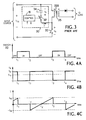
- FIG. 3 Another circuit 30, of the kind described in Vinciarelli, "Optimal Resetting of the Transformer's Core in Single Ended Forward Converters," U. S. Patent No. 4,441,146, (incorporated by reference) is shown in Figure 3.
- This circuit has several advantages, among which are the following: (1) it, too, minimizes the peak voltage seen by the switch, (2) it provides for bipolar transformer 25 core excitation, thereby maximizing utilization of the available flux swing in the transformer's core and allowing for a smaller transformer, and (3) it is essentially lossless.
- circuits 15, 30 of the kinds shown in Figures 2 and 3 When used in single-ended forward converters, core reset circuits 15, 30 of the kinds shown in Figures 2 and 3 will also inherently control the effects of leakage energy by providing a capacitive sink which "snubs" (i.e., clamps) the effect of the release of the leakage energy on switch voltage.
- circuits 15, 30 of the kinds shown in Figures 2 and 3 may be used solely as snubber circuits to manage and control the effects of stored leakage energy.
- flyback converters all of the magnetizing energy stored in the transformer 25 during the time that the primary switch 20 is closed is magnetically coupled into the transformer secondary winding and released to the load after the switch opens.
- Circuits 15, 30 of the kinds shown in Figures 2 and 3 can be modified to correspond to a single-ended flyback topology by simply reversing the polarity of one of the transformer 25 windings) can be used to clamp the voltage which might otherwise be caused by the stored leakage energy.
- the invention features apparatus (and a method) useful in a switching power converter having a transformer and a primary switch for connecting a DC input source to a primary winding of the transformer during a portion of each of a succession of converter operating cycles, the apparatus includes a reset capacitor and a reset switch.
- Reset circuitry cooperates with the reset switch to connect and disconnect the reset capacitor in a manner which provides for resetting the transformer and which allows a current having a non-zero average value to flow in the reset switch.
- Embodiments may include one or more of the following features.
- the reset circuitry may open and close the reset switch.
- the reset circuitry may cause the connecting and disconnecting to occur at times based on switching of the main switch.
- the reset switch may be connected in series with the capacitor.
- the reset circuitry may include circuit elements which inhibit bidirectional energy flow between the capacitor and the transformer.
- the apparatus may only allow transfer of magnetizing energy between the reset capacitor and the transformer if the polarity of the voltage across the reset capacitor is of a particular polarity.
- the apparatus may be connected in parallel with a winding on the transformer.
- the winding may be the primary winding, a secondary winding, or an auxiliary winding.
- the reset switch may be a unidirectional switch (e.g., a MOSFET) in parallel with a unidirectional conducting element (e.g., the intrinsic body diode of the MOSFET), the unidirectional switch and the unidirectional conducting element being arranged to conduct in opposite directions.
- the unidirectional switch may be a MOSFET in series with a series diode, the series diode and the MOSFET being poled to conduct in the same direction.
- the circuit elements may include a reset diode connected in parallel with the capacitor. Bidirectional energy flow may be allowed only if the voltage across the reset capacitor is of a particular polarity.
- the particular polarity may be that which will result in a reversal in the polarity of transformer magnetizing current during the time that the reset switch is closed.
- the reset circuitry may include circuit elements which inhibit bidirectional energy flow between the capacitor and the transformer.
- the circuit elements may include a reset diode connected across a series circuit comprising the reset capacitor and the series diode.
- the switching power converter may be a forward power converter, a zero-current switching converter, or a PWM converter.
- the reset circuitry may open the reset switch prior to the ON period of the primary switch, may close the reset switch during the OFF period of the primary switch, and may keep the reset switch open throughout the ON period of the primary switch.
- the invention features a method for limiting the slew rate in a switching power converter which includes a transformer and a reset circuit of the kind which non-dissipatively recycles the magnetizing energy stored in a transformer during each of a succession of converter operating cycles.
- the method includes sensing the magnetizing current which is flowing in said transformer, and allowing initiation of another converter operating cycle only if the magnetizing current meets a predefined criterion for safe converter operation.
- the predefined criterion may be the magnetizing current passing through a predefined value, e.g., zero.
- Resonance between the transformer and the reset capacitor can be inhibited. Very low dissipation may be achieved.
- the selection of Cr can be made based solely on the operating requirements of the converter.
- oscillation in the reset circuit 30 may generally result in undesirable coupling of energy into the converter output in the form of noise at the frequency fr, or, as seen in Figures 5B to 5D, at a higher frequency associated with resonant ringing of the transformer leakage inductance (Ll, 123, Fig. 6) with both the reset capacitor 34 and the secondary capacitor 60 during the time period that the voltage Vc is positive.
- FIG. 7A Another characteristic of the circuit of Figure 3 is that the maximum allowable converter slew rate (e.g., the rate-of-change of duty cycle), and hence converter response time, are reduced as the value of Cr is increased.
- the damped reset circuit 230 is identical to the circuit of Figure 3 except that a passive damper, consisting of a damper resistor 39 and damper capacitor 35, has been connected across the reset capacitor 34.
- the damper resistor will dissipate energy at frequencies for which the impedance of Cd is low compared to Rd and for which the impedance of Cr is not low relative to Rd. Thus, at both very low and very high frequencies the damper creates little loss.
- waveforms are shown for the converter of Figure 6 with the undamped reset circuit 130 replaced with the damped reset circuit 230 of Figure 8.
- fr is chosen to be well below (e.g., approximately 10% of) the maximum operating frequency of the converter since this puts the "normal" operating frequency range of the converter well above fr and provides for minimum damper dissipation in this range.
- the characteristic frequency, fr, of a ZCS converter operating at frequencies up to 1 MHz would be set to be near 100 KHz. This provides effective damping with relatively little power loss at converter operating frequencies well above fr.
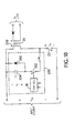
- Figure 10 shows a single-ended converter which includes an improved reset circuit 330.
- the reset switch 332 is opened when the primary switch is closed and vice versa.
- the improved reset circuit 330 differs from the circuits of Figures 3 and 8 by including a diode 350 connected across the reset capacitor 334. By poling the diode as shown, so that the reset capacitor can support positive values of the voltage Vc but cannot support negative values, the diode effectively prevents resonance (e.g., bidirectional energy transfer) from occurring between the reset capacitor 334 and the magnetizing inductance of the transformer 25.
- FIG. 11B show sustained oscillations, either at the characteristic frequency, fr, or at higher frequencies; the absence of the higher frequency oscillation is also an indicator that forward power flow from the reset circuit to the load has been eliminated.
- the decay in the current I in Figure 11B is due to the nonideal characteristics (e.g., parasitic resistances or finite voltage drops) of the diode 350, switch 332, and transformer primary winding 329 -- if all circuit elements were ideal, the current I would remain unchanged until the next operating cycle.
- the parasitic resistances of the reset switches 332, 32 is 0.1 ohm; the parasitic resistance of the transformer primary winding (e.g., primary winding 329 is 0.5 ohm; the diode 350, where used, is a silicon device).
- the average value of the capacitor voltage, Vc, in the circuit of Figure 10 will be approximately equal to Vin*D.
- the diode 350 will not become conductive and the waveforms for the reset circuit of Figure 10 will revert to those shown in Figure 4 for the prior art circuit of Figure 3.
- Preset represents the total amount of power dissipated in the reset circuit (e.g., circuits 230, 330) and Pd represents the loss in the "resonance-control" components used in the particular circuit (e.g., damper resistor 39 in circuit 230; diode 350 in circuit 330).
- loss in the passive damper circuit is strongly influenced by the values of Cr, Cd and Rd, and reductions in Cr result in lower values of Cd and increased amounts of Pd and Preset.
- the values of both Preset and Pd in the improved reset circuit 330 are seen to be much lower than the corresponding losses in the passively damped circuit 230, and the value of loss is only weakly a function of the value of Cr.
- a fundamental and important difference between the prior art reset circuit topology 30 of Figure 3 and the improved topology 330 of Figure 10 is that the average value of the current, I, in the prior art topology must be zero, whereas in the improved topology the average value of I can assume values which are nonzero and positive in the direction of the arrow. This is because all of the current, I, in the topology of Figure 3 must flow in the reset capacitor 34, and, as a result, the voltage Vc can only stabilize at an average value which is consistent with zero average flow of current I.
- the diode 350 provides a path for supporting a positive average value of I. This is how resonance is prevented.
- the improved reset circuit 330 may be placed across a transformer winding other than the primary winding 329.
- the circuit 330 is placed across the secondary winding 331 which delivers power to the load; in Figure 13B it is placed across an auxiliary winding 341.
- a benefit of "direct-coupled" reset e.g., as in Figure 10, where the reset circuit 330 is directly across the winding which is connected to the primary switch 20) is that the reset circuit 330 automatically acts as a snubber for the primary switch when the switch is turned off.
- a benefit of the use of an auxiliary winding 341 (Fig.
- a single reset circuit embodiment e.g., same value of reset capacitor, Cr; the same switch and diode
- a single reset circuit embodiment may be used within converters having widely varying values of both input and output voltage by simply adjusting the relative number of turns on the auxiliary winding to provide a predetermined value of transformer volts-per-turn.
- the reset circuit 330 is connected in other than a direct-coupled configuration, the ability of the circuit to snub the primary switch 20 will be diminished by the leakage inductances between the windings. In such cases care must be used to ensure that the coupling between windings is sufficiently high to prevent excessive voltage spikes on the switch 20.
- the reset switch 332 may, as shown in Figure 14, be embodied as a unipolar switch 339 (the direction of conduction of the current Isw being indicated by the arrow) in parallel with a diode 337. If, as shown in Figure 15A, the switch 332 is embodied as a MOSFET switching device 333, then the intrinsic body diode 337a of the MOSFET device 333 may, under appropriate circumstances, be exploited for use as the diode 337. Suitability of this approach will depend upon the reverse recovery characteristics of the intrinsic body diode (which, for a MOSFET switch, is a function of voltage rating) and the minimum required on-time of the reset switch during the converter operating cycle.
- the reverse recovery time of the intrinsic body diode of an International Rectifier IRFZ15 MOSFET, having a breakdown voltage rating of 60 Volts is 140 nanoseconds, maximum
- the reverse recovery time of the intrinsic body diode of an International Rectifier IRF710 MOSFET, having a breakdown voltage rating of 400 Volts is 520 nanoseconds, maximum.
- the relatively long recovery time of the intrinsic body diode in the cited higher voltage MOSFET would make it unsuitable for use as the diode 337 (Fig. 14) in applications in which the minimum on-time of the reset switch falls below 520 nanoseconds (e.g., in a ZCS converter with a maximum operating frequency around 1 MHz; in most PWM converters at high duty cycles).
- FIG. 15B shows a reset switch 332 embodiment using a MOSFET switch 333 and an external diode 342.
- a series diode 344 is put in series with the MOSFET switch 333.
- FIGS 16A to 16C Several embodiments of an improved reset circuit 330a, 330b, 330c are shown in Figures 16A to 16C, respectively.
- the improved reset circuit 330a incorporates the MOSFET switch 333 of Figure 15A into the circuit topology 330 of Figure 10; in Figure 16B the improved reset circuit 330b incorporates the MOSFET switch 333 and diodes 342, 344 of Figure 15B into the circuit topology 330 of Figure 10.
- the circuit of Figure 16B is modified by connecting the cathode of the reset diode 350 directly to the MOSFET switch 333, rather than to the series diode 344 as is done in Figure 16B. At times at which current is flowing in the reset diode 350, the circuit of Figure 16C will exhibit lower power loss than that of Figure 16B, since the current flow in the circuit of Figure 16C will bypass the series diode 344.
- the diode 344 (Fig. 15B, 16B, 16C) should be a device having a relatively low breakdown voltage rating (e.g., a Schottky diode having a low avalanche voltage rating, Vav).
- a relatively low breakdown voltage rating e.g., a Schottky diode having a low avalanche voltage rating, Vav.
- One reason for this is that diodes having lower breakdown voltages also have lower forward voltage drops and therefore will result in less circuit loss.
- Figures 17A and 17B show converter circuit models 10a, 10b which include, respectively, reset circuits 330a, 330c of the kind shown in Figures 16A and 16C, and inductances 127 which emulate the magnetizing inductance of a transformer.
- the drain-to-source capacitance, Cd 344, and the gate-to-drain capacitance, Cg 348, of the MOSFET 333 (the intrinsic body diode is not shown) and, in Figure 17B, the parasitic junction capacitance, Cj 346, of the external diode 342.
- Vin the converter input voltage
- Im magnetizing current
- the diode 344 has a low breakdown voltage (e.g., 20 Volts) then the diode 344 will avalanche when Im begins to flow in the reset circuit 330c and the capacitances 344, 348 will be discharged until the voltage across the MOSFET (e.g., the voltage across capacitor 344) falls below the breakdown voltage, Vav, of the diode 344, at which point the diode will come out of avalanche and cease conducting. Since Vav is much lower than Vin +Vc the amount of switching loss is substantially reduced. The same reasoning applies to the circuit embodiment of Figure 16B, which will also benefit from use of a series diode 344 having a low breakdown voltage rating.
- a low breakdown voltage e.g. 20 Volts
- the breakdown voltage rating, Vav, of the series diode 344 should not be made too low, however.
- Vs drain-source voltage
- Cd 344 equivalent gate-to-drain capacitance
- the flow of Ig can disrupt control circuitry 16 connected to the FET gate. By keeping Vav at a suitable value (e.g., 20 V) this problem can be avoided with minimal increase in switching losses.
- a suitable value e.g. 20 V
- the flow of Ig may be bypassed around the control circuitry 16 by adding a high-speed diode 347 (e.g., a Schottky diode) across the gate-to-source terminals of the MOSFET.
- Controlling the reset switch 332 (Fig. 10) in the improved reset circuit 330 is essentially the same as controlling the switch 32 in the prior art converter of Fig. 3.
- the reset switch 332 must be turned on after the primary switch 20 opens and must be off when the primary switch closes. If a reset switch of the kind shown in Figures 14 and 15 is used, the timing of the closure of the reset switch is not critical since the diode (337, Fig. 14) will begin to conduct magnetizing current Im as soon as the current commutates into the reset circuit 330.
- closure of the reset switch must not be allowed to occur while the primary switch is conductive as this can cause catastrophic failure of the converter. Therefore it is beneficial to provide means for sensing that the primary switch 20 has opened and enable closure of the reset switch only when this signal is present.
- Figures 18A and 18B Ways to sense the state of the primary switch are shown in Figures 18A and 18B.
- a reset circuit of the kind shown in Figure 16B is shown connected to a transformer 25 and a primary switch 20.
- a sense resistor 402 of a relatively small value Rs, is connected in series with the diode 342.
- the primary switch 20 opens and magnetizing current begins flowing, as a negative flow of the current I, in the diode 342 the voltage, Vm, across the resistor will go negative and this may be used to sense that the primary switch is no longer conductive.
- One drawback of the method of Figure 18A is that the use of the resistor will cause power loss.
- FIG. 18B A preferred method for sensing the state of the primary switch as a means of safely enabling the reset switch is shown in Figure 18B.
- a diode 410 a large value resistor 412 and bias source 414, of voltage Vb ⁇ Vin, are used as sensing elements.
- Vs a small voltage value
- the switch 333 begins to carry the current and the voltage Vs increases to a value Vk, which is more positive than Vz and approximately equal to the voltage drop across the switch, Vsw.
- Vk the voltage drop across the switch
- the current which flows in the transformer primary, Ip will, as shown in Figures 21A through 21C, consist of a magnetizing current component, Im, and a forward current component, Io (e.g., in a ZCS converter, as shown in Fig. 21B, Io is the approximately sinusoidal portion of the transformer primary current which is reflected into the secondary winding).
- Io a forward current component
- the primary current, Ip is negative, and this flow of negative current will discharge the parasitic capacitance 343 of the primary switch 20 if the switch is off.
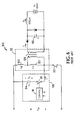
- FIG. 20 shows a reset switch controller 520 which incorporates some of the features described above.
- a primary switch controller 530 delivers Primary Switch Enable (MS) pulses 511 indicating when the primary switch 20 is to be turned on. Assuming that the reset switch 332 is turned on (e.g., the Reset Switch signal output of flip-flop 502 is high), delivery of a PSE pulse will cause both flip-flops 502, 504 to be reset via their reset inputs. This will cause the Reset Switch signal 501 to go low, initiating turn-off of the reset switch, and will also cause the Disable signal 515 to go high.
- MS Primary Switch Enable
- the Primary Switch Controller 530 will not deliver another PSE pulse unless the Disable signal 515 is low.
- the result is that the primary switch 20 is turned on a short time after the reset switch is turned off.
- the dead time is determined by circuit propagation times and the delay introduced by delay element 510 -- in a typical 1 Mhz ZCS converter the delay might be a few tens of nanoseconds. Provided that the delay is relatively short, its value is non-critical since the transformer magnetizing current which flows during the dead time will beneficially charge parasitic capacitances associated with both switches.
- This causes the output of the comparator 500 to go low, bringing the Disable signal low. This, in turn, signals the primary switch controller 530 that it is safe for it to deliver a subsequent PSE pulse 511. Some time later (e.g., at approximately time t tf) another PSE pulse is generated and the cycle is repeated.
- topologies and circuits described above may be adapted for use in other than single-ended converters (e.g.; full bridge or half-bridge converters).
Abstract
Description
- This invention relates to control of stored magnetic energy in power converter transformers.
- In one class of power converters, called single-ended switching power converters (10, Figure 1), a
primary switching element 20 is used to repetitively connect an input source to theprimary winding 329 of a power transformer 25 (Figure 1) during a portion of each of a series of converter operating cycles. In some such converters, called "single-ended forward converters," forward energy transfer from the input source toward the load occurs during the time that the switch is closed.
In other topologies, called "single-ended flyback converters", energy is stored in the transformer during the time that the switch is closed and is transferred forward to the load after the switch is opened. In yet other single-ended converters a portion of the energy may be transferred during both the on and off times of the switch. In general, practical converters of this kind must incorporate circuitry for managing the effects of magnetic energy storage in the transformer. For example, in converters in which energy is transferred forward during the on-time of the switch, circuitry is typically included to deal with the magnetizing energy which is stored in the transformer at the time that the switch is opened (e.g., to provide means for "resetting" the transformer); more generally, the effects of magnetic energy storage in the leakage inductance of the transformer must also be managed, e.g., to prevent the energy stored in the leakage field from overstressing the switch when the switch is turned off. - A wide variety of reset circuits (also called core reset circuits because almost all switching power converter transformers include a magnetic core), for use in single-ended forward converters, are described in the literature. These circuits differ in terms of their efficiency, cost and impact on converter power density. One
such circuit 15, shown in Figure 2, is described in Clemente, et al., "A Universal 100 KHz Power Supply Using a Single HEXFET," International Rectifier Corporation Applications Note AN-939, December 1980. One of the advantages of this circuit is that it can maintain the minimal value of peak switch voltage consistent with converter input voltage and duty cycle; one of its disadvantages is that it is dissipative and therefore compromises both converter efficiency and power density. Anothercircuit 30, of the kind described in Vinciarelli, "Optimal Resetting of the Transformer's Core in Single Ended Forward Converters," U. S. Patent No. 4,441,146, (incorporated by reference) is shown in Figure 3. This circuit has several advantages, among which are the following: (1) it, too, minimizes the peak voltage seen by the switch, (2) it provides forbipolar transformer 25 core excitation, thereby maximizing utilization of the available flux swing in the transformer's core and allowing for a smaller transformer, and (3) it is essentially lossless. - When used in single-ended forward converters,
core reset circuits circuits transformer 25 during the time that theprimary switch 20 is closed is magnetically coupled into the transformer secondary winding and released to the load after the switch opens. While this provides a natural mechanism for reducing the magnetizing energy to zero it does not provide a mechanism for managingtransformer 25 leakage energy, which can causeexcessive switch 20 voltage when theswitch 20 is opened.Circuits transformer 25 windings) can be used to clamp the voltage which might otherwise be caused by the stored leakage energy. For example, in Ogden, "Improved High Frequency Switching in Coupled Inductor Power Supplies,"European Patent Application 0 350 297, a circuit essentially identical to that of thecircuit 30 of Figure 2 is used to both clamp the leakage inductance energy in a flyback converter and reroute it forward toward the load. - In an aspect, the invention features apparatus (and a method) useful in a switching power converter having a transformer and a primary switch for connecting a DC input source to a primary winding of the transformer during a portion of each of a succession of converter operating cycles, the apparatus includes a reset capacitor and a reset switch. Reset circuitry cooperates with the reset switch to connect and disconnect the reset capacitor in a manner which provides for resetting the transformer and which allows a current having a non-zero average value to flow in the reset switch.
- Embodiments may include one or more of the following features. The reset circuitry may open and close the reset switch. The reset circuitry may cause the connecting and disconnecting to occur at times based on switching of the main switch. The reset switch may be connected in series with the capacitor. The reset circuitry may include circuit elements which inhibit bidirectional energy flow between the capacitor and the transformer. The apparatus may only allow transfer of magnetizing energy between the reset capacitor and the transformer if the polarity of the voltage across the reset capacitor is of a particular polarity. The apparatus may be connected in parallel with a winding on the transformer. The winding may be the primary winding, a secondary winding, or an auxiliary winding. The reset switch may be a unidirectional switch (e.g., a MOSFET) in parallel with a unidirectional conducting element (e.g., the intrinsic body diode of the MOSFET), the unidirectional switch and the unidirectional conducting element being arranged to conduct in opposite directions. The unidirectional switch may be a MOSFET in series with a series diode, the series diode and the MOSFET being poled to conduct in the same direction. The circuit elements may include a reset diode connected in parallel with the capacitor. Bidirectional energy flow may be allowed only if the voltage across the reset capacitor is of a particular polarity. The particular polarity may be that which will result in a reversal in the polarity of transformer magnetizing current during the time that the reset switch is closed. The reset circuitry may include circuit elements which inhibit bidirectional energy flow between the capacitor and the transformer. The circuit elements may include a reset diode connected across a series circuit comprising the reset capacitor and the series diode. The switching power converter may be a forward power converter, a zero-current switching converter, or a PWM converter. The reset circuitry may open the reset switch prior to the ON period of the primary switch, may close the reset switch during the OFF period of the primary switch, and may keep the reset switch open throughout the ON period of the primary switch.
- In an alternative aspect, the invention features a method for limiting the slew rate in a switching power converter which includes a transformer and a reset circuit of the kind which non-dissipatively recycles the magnetizing energy stored in a transformer during each of a succession of converter operating cycles. The method includes sensing the magnetizing current which is flowing in said transformer, and allowing initiation of another converter operating cycle only if the magnetizing current meets a predefined criterion for safe converter operation. The predefined criterion may be the magnetizing current passing through a predefined value, e.g., zero.
- Among the potential advantages are the following: Resonance between the transformer and the reset capacitor can be inhibited. Very low dissipation may be achieved. The selection of Cr can be made based solely on the operating requirements of the converter.
- The invention is hereinafter more particularly described by way of example only with reference to the accompanying drawings.
- In the drawings:-
- Fig. 1 shows a schematic of a single-ended switching power converter.
- Fig. 2 shows a schematic of a converter which incudes a dissipative prior art circuit useful for performing transformer resetting and snubbing.
- Fig. 3 shows a schematic of a converter which includes a non-dissipative prior art circuit topology which is useful for performing transformer resetting and snubbing.
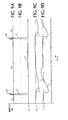
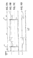
- Figs. 4A to 4C show operating waveforms for the circuit of Fig. 3.
- Figs. 5A through 5D show additional operating waveforms for the circuit of Fig. 3.
- Fig. 6 shows a schematic of a single-ended zero-current switching converter which includes a reset circuit of the kind shown in Fig. 3.
- Figs. 7A and 7B show the effect of a sudden change in operating frequency on the waveform of Fig. 4C.
- Fig. 8 shows a schematic of a single-ended converter which includes a prior art damped reset circuit topology.
- Figs. 9A to 9D show operating waveforms for the converter of Fig. 8.
- Fig. 10 shows a schematic of a single-ended converter which includes an example of an improved reset circuit topology according to the present invention.
- Figs. 11A to 11D show operating waveforms for the converter of Fig. 10.
- Figs. 12A and 12B show tables which compare losses in the damped reset circuit of Fig. 8 to the improved reset circuit of Fig. 10.
- Figs. 13A and 13B show schematics which indicate alternate connections for the reset circuits of Figs. 3, 8 and 10.
- Fig. 14 shows an equivalent circuit of a switch for use in the circuit of Figs. 3, 8 and 10.
- Figs. 15A and 15B show embodiments of the switch of Fig. 14 which include a MOSFET.
- Figs. 16A to 16C show alternate embodiments of the improved reset circuit topology of Fig. 10.
- Figs. 17A and 17B show schematic models of converters which include reset circuits of the kind shown in Figs. 16A and 16C, respectively.
- Figs. 18A and 18B show circuit schematics illustrating ways to sense when the primary switch has become non-conductive.
- Figs. 19A and 19B show waveforms for the circuit of Fig. 18B.
- Fig. 20 is a circuit schematic of a reset switch controller.
- Figs. 21A to 21C show current waveforms for a ZCS converter.
-
- Waveforms for the
core reset circuit 30 of Figure 3 in a single ended forward converter under steady-state operating conditions are shown in Figures 4A through 4C, assuming ideal circuit components and areset capacitor 34 of sufficiently large value, Cr, so that the characteristic frequency, fr, of the resonant circuit consisting of thereset capacitor 34 and the magnetizing inductance of the transformer 25 (of value Lm) is well below the converter operating frequency, fop (e.g., fr << fop, where fr = 1/(2*pi*sqrt(Lm*Cr) and fop = 1/(t3-t1)). When aprimary switch 20, connected to a primary winding 329 of thetransformer 25, is turned on, thereset switch 32 is off (by means of control circuitry 16) and vice versa. When thereset switch 32 is turned on at the end of an operating cycle (e.g., at time t = t2), energy stored as magnetizing current in the transformer (e.g., current I = -Im at time t2, Figure 4C) is resonantly transferred to thecapacitor 34 until, at time t = t3, at the beginning of the next converter operating cycle, the current has reversed (I = Im). Under a particular set of steady-state operating conditions (e.g., Vin and duty cycle, D = ton/toff) the capacitor voltage Vc will converge on a value equal to Vin*D and the peak voltage seen by the switch, Vp (Fig. 4B), will be equal to Vin + Vc = Vin(1+D). Since Tr = 1/fr is assumed to be large relative to the operating period of the converter, both of these voltages will be essentially constant throughout the time that the primary switch is open and the peak voltage seen by theswitch 20 will therefore be minimized. - Core reset circuits of the kind shown in Figure 3 offer several important benefits. Recirculation of energy between circuit elements allows these circuits to operate as magnetizing current "mirrors," producing both a current and flux reversal during the reset interval (e.g., t = t2 to t = t3). As a result, circuits of this kind not only minimize loss, but effectively double the available "volt-time" product of the core and allow for an approximately two-fold reduction in the size of the core.
- Because the core reset circuit of Figure 3 is based upon a resonant circuit, however, steps must be taken to prevent resonant effects from adversely affecting converter operation. In practical switching power converters, for example, neither the input voltage, Vin, nor the duty cycle, D, will be constant and, as a result, the average value of the voltage Vc will vary with changes in Vin and D. For a
circuit 30 of the kind shown in Figure 3, however, changes in the average value of Vc may be accompanied by a persistent oscillation in Vc at the resonant frequency fr. - In converters in which operating frequency varies (e.g., in zero-current switching (ZCS) converters of the kind described in Vinciarelli, "Forward Converter Switching at Zero Current," U. S. Patent No. 4,415,959, incorporated by reference) additional problems may arise, especially as the converter operating frequency drops to values comparable to, or below, the frequency fr. In such cases, the waveforms of Figure 4 will no longer apply. Rather, as illustrated in Figures 5A to 5D (for a zero-current switching converter having an equivalent circuit and the equivalent circuit values shown in Figure 6 operating at a frequency, fop = 50 KHz, which is below the characteristic frequency of the
reset circuit 130, fr = 84 KHz) both the reset capacitor voltage, Vc (Fig. 5C), and the magnetizing current, I (Fig. 5D) rise and fall sinusoidally and assume both positive and negative values (although, as described earlier for higher converter operating frequencies, the average value of the capacitor voltage, Vc, over a time period which is long compared to a converter operating cycle and under steady state operating conditions, will still be approximately equal to Vin*D). With reference to Figures 5B and D and Figure 6, during time periods that the voltage Vc goes positive (e.g., between times tp1 and tp2, Figure 5) energy can be transferred from thereset circuit 30 via thetransformer 25 forward to the converter load. This will effectively cause a change in the open-loop gain of the converter and can contribute to, or cause, closed-loop instability. In addition, oscillation in thereset circuit 30 may generally result in undesirable coupling of energy into the converter output in the form of noise at the frequency fr, or, as seen in Figures 5B to 5D, at a higher frequency associated with resonant ringing of the transformer leakage inductance (Ll, 123, Fig. 6) with both thereset capacitor 34 and thesecondary capacitor 60 during the time period that the voltage Vc is positive. - Another characteristic of the circuit of Figure 3 is that the maximum allowable converter slew rate (e.g., the rate-of-change of duty cycle), and hence converter response time, are reduced as the value of Cr is increased. This is illustrated in Figures 7A and 7B for a
circuit 30 of the kind shown in Figure 3 operating in a variable frequency converter. As indicated in the Figures, the converter operating period is T1 until time t = ta, after which the period decreases sharply to a lower value T2. If thereset capacitor 34 is assumed to be large enough so that the voltage across the capacitor, Vc, cannot change substantially over a time span corresponding to several converter operating cycles, then the peak variation in magnetizing current, ΔIp, during the OFF times of theprimary switch 20 will not change substantially over the same time span. Under these circumstances, a sufficiently large reduction in operating period will, as illustrated in Figure 7B, result in a cycle-by-cycle increase in the peak negative excursion of the magnetizing current, I, sufficient to cause transformer saturation within a few operating cycles. Smaller values of Cr allow for greater cycle-by-cycle adaptation in Vc which, in turn, would allow for faster duty cycle slewing and faster converter response time. The same principle applies in a constant frequency, pulse-width modulated (PWM) converter. - One way to minimize the effects of resonance in the reset circuit of Figure 3 is to damp the circuit, as illustrated in Figure 8. In the Figure, the
damped reset circuit 230 is identical to the circuit of Figure 3 except that a passive damper, consisting of adamper resistor 39 anddamper capacitor 35, has been connected across thereset capacitor 34. The damper resistor will dissipate energy at frequencies for which the impedance of Cd is low compared to Rd and for which the impedance of Cr is not low relative to Rd. Thus, at both very low and very high frequencies the damper creates little loss. In Figures 9A through 9D, for example, waveforms are shown for the converter of Figure 6 with theundamped reset circuit 130 replaced with thedamped reset circuit 230 of Figure 8. Circuit values are Cr = 0.1 microfarad, Cd = 0.22 microfarad, and Rd = 20 ohms. Comparing the waveforms of Figure 9 to those of Figure 5 indicates that both the resonant reset circuit oscillations and the parasitic high frequency oscillations have been significantly reduced. Power flow from the reset circuit to the load has also been substantially reduced. - Effective damping has been achieved by setting the value of the damper capacitor, Cd, to approximately two times the value of Cr, and setting the damper resistor value, Rd, so that the damper frequency, fd = 1/Rd*Cd, is equal to about one-half the undamped characteristic frequency fr. To avoid excessive dissipation in the damper resistor, fr is chosen to be well below (e.g., approximately 10% of) the maximum operating frequency of the converter since this puts the "normal" operating frequency range of the converter well above fr and provides for minimum damper dissipation in this range. Thus, the characteristic frequency, fr, of a ZCS converter operating at frequencies up to 1 MHz (or of a constant frequency PWM converter operating at a similar frequency) would be set to be near 100 KHz. This provides effective damping with relatively little power loss at converter operating frequencies well above fr.
- In practice, however, use of the damped reset circuit requires balancing several sometimes conflicting requirements. On the one hand, use of a low value for Cr is generally desirable as it provides for a higher allowable converter slew rates and increases the value of fr above the crossover frequency of the converter. On the other hand, low values of Cr result in increased dissipation in the damper resistor. For example, if the
damped reset circuit 230 of Figure 8 is used in place of theundamped circuit 130 in the ZCS converter of Figure 6, and if Cr = 0.1 microfarad, Cd = 0.22 microfarad, and Rd = 20 ohms, then, as indicated in the table in Figure 12B, the dissipation in thedamper resistor 39 at an operating period Top = 3 microseconds (with the converter delivering 217 Watts) is approximately Pd = 80 milliwatts. When the operating frequency is reduced to 50 KHz (with the converter delivering 15 Watts), the dissipation, indicated in the table of Figure 12A, rises to approximately Pd = 2.4 Watts. If, however, the component values are adjusted to Cr = 0.01 microfarad, Cd = 0.22 microfarad and Rd = 120 ohms, which provides the same damping at a higher value of fr, then, as indicated in the Table of Figure 12B, the dissipation at Top = 3 microseconds rises to Pd = 3.0 Watts and the dissipation at 50 KHz (Table of Figure 12A) rises to 2.7 Watts. Thus, while the lower value of Cr would allow for improvement in converter response time it would also result in an unacceptable increase in power loss (e.g., the additional 3 Watts of loss at 217 Watts represents an approximate reduction in conversion efficiency of 1.5%). - Figure 10 shows a single-ended converter which includes an
improved reset circuit 330. Like the circuits of Figures 3 and 8, thereset switch 332 is opened when the primary switch is closed and vice versa. Theimproved reset circuit 330 differs from the circuits of Figures 3 and 8 by including adiode 350 connected across thereset capacitor 334. By poling the diode as shown, so that the reset capacitor can support positive values of the voltage Vc but cannot support negative values, the diode effectively prevents resonance (e.g., bidirectional energy transfer) from occurring between thereset capacitor 334 and the magnetizing inductance of thetransformer 25. - The beneficial effects of the diode in preventing resonance may be seen, in part, by comparing the waveforms in Figure 11 to those in Figures 9 and 5. In Figure 11, waveforms are shown for the converter of Figure 6 in which the
undamped reset circuit 130 is replaced with theimproved reset circuit 330 of Figure 10. Thereset capacitor 334 value is Cr = 0.1 microfarad. Comparing Figures 11A through 11D with the corresponding waveforms of Figures 9 and 5 it can be seen that the waveforms in the improved circuit are better behaved and more predictable than the waveforms in the other Figures -- neither Vc (Fig. 11D) nor I (Fig. 11B) show sustained oscillations, either at the characteristic frequency, fr, or at higher frequencies; the absence of the higher frequency oscillation is also an indicator that forward power flow from the reset circuit to the load has been eliminated. Figure 11D also clearly shows that the reset capacitor voltage does not assume positive values. Rather, as Vc passes through zero volts (e.g., after t = to. Fig. 11) thediode 350 becomes conductive, resonant energy transfer is terminated and thediode 350 conducts the magnetizing current I (Fig. 11B) until the beginning of the next operating cycle. The decay in the current I in Figure 11B is due to the nonideal characteristics (e.g., parasitic resistances or finite voltage drops) of thediode 350,switch 332, and transformer primary winding 329 -- if all circuit elements were ideal, the current I would remain unchanged until the next operating cycle. (In all of the circuits of Figures 10, 8 and 6 the parasitic resistances of the reset switches 332, 32 is 0.1 ohm; the parasitic resistance of the transformer primary winding (e.g., primary winding 329 is 0.5 ohm; thediode 350, where used, is a silicon device). As in the reset circuits of Figures 3 and 8, the average value of the capacitor voltage, Vc, in the circuit of Figure 10, over a time frame which is long with respect to a converter operating cycle and under steady-state operating conditions, will be approximately equal to Vin*D. At converter operating frequencies which are substantially higher than the characteristic frequency fr, thediode 350 will not become conductive and the waveforms for the reset circuit of Figure 10 will revert to those shown in Figure 4 for the prior art circuit of Figure 3. - While selection of the value of the reset capacitor in the damped reset circuit (Figure 8) involved tradeoffs between response time and dissipation, these tradeoffs do not apply to the
improved circuit 330 of Figure 10. The improved circuit exhibits such markedly lower dissipation that the value of Cr may be chosen solely on the basis of desired converter performance criteria (e.g., response time) and the peak voltage limits imposed by the converter switches. This is indicated in the Tables of Figures 12A and 12B in which losses in the improved reset circuit of Figure 10 are compared to losses in the damped reset circuit of Figure 8 for different values of damper components (35, 35, Figure 8) and at different operating frequencies. In the Tables, Preset represents the total amount of power dissipated in the reset circuit (e.g.,circuits 230, 330) and Pd represents the loss in the "resonance-control" components used in the particular circuit (e.g.,damper resistor 39 incircuit 230;diode 350 in circuit 330).
As discussed earlier, loss in the passive damper circuit is strongly influenced by the values of Cr, Cd and Rd, and reductions in Cr result in lower values of Cd and increased amounts of Pd and Preset. The values of both Preset and Pd in theimproved reset circuit 330 are seen to be much lower than the corresponding losses in the passively dampedcircuit 230, and the value of loss is only weakly a function of the value of Cr. The dependence of Pd on operating frequency is a result of the increased peak-to-peak swing in the magnetizing current, I, flowing in thenonideal diode 350 at low converter operating frequencies. In practice, the losses are essentially insignificant. Of greatest importance is the fact that selection of the value of Cr in the improved reset circuit need not be traded off against circuit dissipation. Rather, the value of Cr in theimproved circuit 330 may be selected based solely upon converter performance requirements (e.g., desired converter slew rates; input voltage and load range) and the voltage rating of theprimary switch 20. - A fundamental and important difference between the prior art
reset circuit topology 30 of Figure 3 and theimproved topology 330 of Figure 10 is that the average value of the current, I, in the prior art topology must be zero, whereas in the improved topology the average value of I can assume values which are nonzero and positive in the direction of the arrow. This is because all of the current, I, in the topology of Figure 3 must flow in thereset capacitor 34, and, as a result, the voltage Vc can only stabilize at an average value which is consistent with zero average flow of current I. In the improved topology, thediode 350 provides a path for supporting a positive average value of I. This is how resonance is prevented. In the topology of Figure 3 resonant energy transfer results in the current I passing bidirectionally between thecapacitor 34 and the magnetizing inductance of the transformer. In the topology of Figure 10 this is impossible -- as the voltage Vc (Fig. 10) attempts to go negative thediode 350 begins to bypass current around thecapacitor 334, effectively replacing the capacitor with a short circuit. Energy in the magnetizing inductance is no longer transferred to the capacitor and the current, I, continues to flow in the inductor at an essentially constant value. As noted above, however, in non-ideal embodiments, losses in circuit elements will cause a decline in the value of I. - As shown in Figures 13A and 13B, the
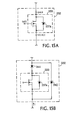
improved reset circuit 330 may be placed across a transformer winding other than the primary winding 329. For example, in Figure 13A thecircuit 330 is placed across the secondary winding 331 which delivers power to the load; in Figure 13B it is placed across an auxiliary winding 341. A benefit of "direct-coupled" reset (e.g., as in Figure 10, where thereset circuit 330 is directly across the winding which is connected to the primary switch 20) is that thereset circuit 330 automatically acts as a snubber for the primary switch when the switch is turned off. On the other hand, a benefit of the use of an auxiliary winding 341 (Fig. 13B) is that a single reset circuit embodiment (e.g., same value of reset capacitor, Cr; the same switch and diode) may be used within converters having widely varying values of both input and output voltage by simply adjusting the relative number of turns on the auxiliary winding to provide a predetermined value of transformer volts-per-turn. However, where thereset circuit 330 is connected in other than a direct-coupled configuration, the ability of the circuit to snub theprimary switch 20 will be diminished by the leakage inductances between the windings. In such cases care must be used to ensure that the coupling between windings is sufficiently high to prevent excessive voltage spikes on theswitch 20. - In practice the
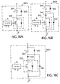
reset switch 332 may, as shown in Figure 14, be embodied as a unipolar switch 339 (the direction of conduction of the current Isw being indicated by the arrow) in parallel with adiode 337.
If, as shown in Figure 15A, theswitch 332 is embodied as aMOSFET switching device 333, then theintrinsic body diode 337a of theMOSFET device 333 may, under appropriate circumstances, be exploited for use as thediode 337. Suitability of this approach will depend upon the reverse recovery characteristics of the intrinsic body diode (which, for a MOSFET switch, is a function of voltage rating) and the minimum required on-time of the reset switch during the converter operating cycle. For example, the reverse recovery time of the intrinsic body diode of an International Rectifier IRFZ15 MOSFET, having a breakdown voltage rating of 60 Volts, is 140 nanoseconds, maximum, whereas the reverse recovery time of the intrinsic body diode of an International Rectifier IRF710 MOSFET, having a breakdown voltage rating of 400 Volts, is 520 nanoseconds, maximum. The relatively long recovery time of the intrinsic body diode in the cited higher voltage MOSFET would make it unsuitable for use as the diode 337 (Fig. 14) in applications in which the minimum on-time of the reset switch falls below 520 nanoseconds (e.g., in a ZCS converter with a maximum operating frequency around 1 MHz; in most PWM converters at high duty cycles). On the other hand, the faster recovery time of the body diode in the lower voltage MOSFET would allow it to be used in a fairly broad array of applications. In cases where theintrinsic body diode 337 cannot be used as thediode 337, an external diode may be used. Figure 15B shows areset switch 332 embodiment using aMOSFET switch 333 and anexternal diode 342. To prevent conduction by theintrinsic body diode 337a when current is flowing in theexternal diode 342, aseries diode 344 is put in series with theMOSFET switch 333. - Several embodiments of an
improved reset circuit improved reset circuit 330a incorporates theMOSFET switch 333 of Figure 15A into thecircuit topology 330 of Figure 10; in Figure 16B theimproved reset circuit 330b incorporates theMOSFET switch 333 anddiodes circuit topology 330 of Figure 10. In theembodiment 330c of Figure 16C, the circuit of Figure 16B is modified by connecting the cathode of thereset diode 350 directly to theMOSFET switch 333, rather than to theseries diode 344 as is done in Figure 16B. At times at which current is flowing in thereset diode 350, the circuit of Figure 16C will exhibit lower power loss than that of Figure 16B, since the current flow in the circuit of Figure 16C will bypass theseries diode 344. - As a practical matter the diode 344 (Fig. 15B, 16B, 16C) should be a device having a relatively low breakdown voltage rating (e.g., a Schottky diode having a low avalanche voltage rating, Vav). One reason for this is that diodes having lower breakdown voltages also have lower forward voltage drops and therefore will result in less circuit loss. Another reason is illustrated with reference to Figures 17A and 17B, which show
converter circuit models circuits inductances 127 which emulate the magnetizing inductance of a transformer. Also indicated in the Figures are certain parasitic capacitances: the drain-to-source capacitance,Cd 344, and the gate-to-drain capacitance,Cg 348, of the MOSFET 333 (the intrinsic body diode is not shown) and, in Figure 17B, the parasitic junction capacitance,Cj 346, of theexternal diode 342. We assume that the converter input voltage, Vin, is relatively high (e.g., 300 Volts), that theprimary switch 20 has just opened and that magnetizing current, Im, has begun to flow, in the direction indicated, in bothreset circuits Cg 348 andCd 344 and then continue to flow in the intrinsic body diode (not shown) of theMOSFET 333. Thus, when the MOSFET is turned on it is done so at essentially zero voltage and switching losses are essentially eliminated. In the circuit of Figure 17B, however, if theseries diode 344 has a high breakdown voltage rating, then the flow of magnetizing current, Im, will discharge thejunction capacitance 346 of theexternal diode 342 but the blocking action of theseries diode 344 will prevent discharging of thecapacitances Cg 348 andCd 344 of theMOSFET 333. These capacitances will remain charged to a voltage equal to Vin + Vc, where Vc is the value of thereset capacitor 334 voltage at the time that theswitch 20 is turned off. When thereset MOSFET 333 is subsequently turned on, the energy stored in these capacitances will be dissipated in the MOSFET as switching losses. If however, thediode 344 has a low breakdown voltage (e.g., 20 Volts) then thediode 344 will avalanche when Im begins to flow in thereset circuit 330c and thecapacitances diode 344, at which point the diode will come out of avalanche and cease conducting. Since Vav is much lower than Vin +Vc the amount of switching loss is substantially reduced. The same reasoning applies to the circuit embodiment of Figure 16B, which will also benefit from use of aseries diode 344 having a low breakdown voltage rating. - The breakdown voltage rating, Vav, of the
series diode 344 should not be made too low, however. As the drain-source voltage, Vs, across the MOSFET (Figs. 17A, 17B) drops, the value of the equivalent gate-to-drain capacitance,Cd 344, goes up. This will result in an increase in the parasitic gate current Ig as the value of Vav falls. In practice, allowing the voltage to decline to near zero volts (e.g., as would happen in the circuit of Fig. 17A) can result in substantial transient values of Ig (e.g., to approximately 2 Amperes for a HEX1 size MOSFET die in a 200 Watt ZCS converter). The flow of Ig can disruptcontrol circuitry 16 connected to the FET gate. By keeping Vav at a suitable value (e.g., 20 V) this problem can be avoided with minimal increase in switching losses. Inreset circuits 330a of the kind shown in Figure 17A, where the series diode is not used, the flow of Ig may be bypassed around thecontrol circuitry 16 by adding a high-speed diode 347 (e.g., a Schottky diode) across the gate-to-source terminals of the MOSFET. - Controlling the reset switch 332 (Fig. 10) in the
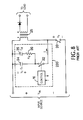
improved reset circuit 330 is essentially the same as controlling theswitch 32 in the prior art converter of Fig. 3. Thereset switch 332 must be turned on after theprimary switch 20 opens and must be off when the primary switch closes. If a reset switch of the kind shown in Figures 14 and 15 is used, the timing of the closure of the reset switch is not critical since the diode (337, Fig. 14) will begin to conduct magnetizing current Im as soon as the current commutates into thereset circuit 330. Delay between opening of theprimary switch 20 and closure of thereset switch 332 will not affect circuit operation provided only that the reset switch is ready to conduct current when the current eventually reverses and the diode becomes non-conductive (e.g., the switch must be conductive at and after time t = tx in Figures 4C, 5D, 7B, 9D, 11B). On the other hand, closure of the reset switch must not be allowed to occur while the primary switch is conductive as this can cause catastrophic failure of the converter. Therefore it is beneficial to provide means for sensing that theprimary switch 20 has opened and enable closure of the reset switch only when this signal is present. - Ways to sense the state of the primary switch are shown in Figures 18A and 18B. In the Figures a reset circuit of the kind shown in Figure 16B is shown connected to a
transformer 25 and aprimary switch 20. In Figure 18A asense resistor 402, of a relatively small value Rs, is connected in series with thediode 342. When theprimary switch 20 opens and magnetizing current begins flowing, as a negative flow of the current I, in thediode 342 the voltage, Vm, across the resistor will go negative and this may be used to sense that the primary switch is no longer conductive. One drawback of the method of Figure 18A is that the use of the resistor will cause power loss. - A preferred method for sensing the state of the primary switch as a means of safely enabling the reset switch is shown in Figure 18B. In the Figure a
diode 410, alarge value resistor 412 andbias source 414, of voltage Vb < Vin, are used as sensing elements. Prior to opening the primary switch (e.g., prior to time t=tm in Figures 19A and 19B) the voltage, Vr, across thediode 342 is greater than Vin, thediode 410 is reverse biased and Vs = Vb. At time t = tm, when theprimary switch 20 becomes non-conductive, the magnetizing current begins flowing, as a negative flow of current I, indiode 342 and the sense voltage, Vs, drops to a small voltage value, Vz, equal to the difference between the drops in the twodiodes 342, 410 (which may be assumed to be close to zero volts). The drop in Vs may be sensed as an indicator that the primary switch has opened. - With reference to Figure 7, it has already been noted that premature initiation of primary switch turn-on can cause
transformer 25 saturation, and that this possibility requires that control be asserted over maximum converter slew rate. One way to do this is to sense the magnetizing current during the reset interval and inhibit initiation of the next converter operating cycle (e.g., the next turn-on of the primary switch) until the magnetizing current is deemed to be at a safe level. In one example of setting acceptable criteria for enabling turn-on of the main switch, we note that during the first few operating cycles following application of input power to a typical power converter the variation in magnetizing current will not be symmetrical about zero current, but will, during the time the primary switch is turned on, increase from essentially zero current up to absolute values which can equal ΔIpmax (Figs. 7, 19). As a result, the transformer is typically designed to be able to withstand at least this absolute value of current without saturating. Therefore, with reference to Figures 7 and 19, it would be safe to turn the primary switch on at any time after time t = tx as this will ensure that the absolute value of magnetizing current during the next cycle will not exceed ΔIpmax. Use of a strategy of this kind will automatically control the slew rate of the converter in such a way that maximum slew rates are always achieved consistent with safe converter operation. - One way of sensing the magnetizing current is to measure it directly, as is done in the circuit of Figure 18A in which the voltage Vm = I*Rs. Slew rate may be controlled by comparing Vm to some set of predetermined safe operating criteria, and inhibiting or enabling primary switch turn-on based upon that comparison. Alternatively, a measurement indicative of the value of magnetizing current may also be used. For example, the circuit of Figure 18B may be used to derive a signal which indicates when the magnetizing current crosses through zero. With reference to Figure 19B, at time t = tx, the magnetizing current has increased by ΔIp/2 and is crossing through zero. At this time, the
switch 333 begins to carry the current and the voltage Vs increases to a value Vk, which is more positive than Vz and approximately equal to the voltage drop across the switch, Vsw. Assuming that the converter transformer can accommodate an absolute value of magnetizing current equal to ΔIp, the increase in the voltage Vs at time t = tx may be used to indicate that it is safe to enable initiation of the next converter operating cycle. - It is also to be noted that, if the magnetizing current is scaled properly, operation of the reset circuit may be exploited to allow the primary switch to be switched on at zero-voltage. Assume, for example, that the circuits of Figures 18A or 18B form a portion of a ZCS converter, that the
primary switch 20 is of the kind described with reference to Figure 14 above, that theprimary switch 20 has aparasitic capacitance Cd 343, and that the reset switch 333 (Fig. 18) is opened at time t = tf (e.g., as in Fig. 19). At t = tf, magnetizing current will be flowing as a negative flow of transformer primary current Ip. Following time t = tf, the current which flows in the transformer primary, Ip, will, as shown in Figures 21A through 21C, consist of a magnetizing current component, Im, and a forward current component, Io (e.g., in a ZCS converter, as shown in Fig. 21B, Io is the approximately sinusoidal portion of the transformer primary current which is reflected into the secondary winding). Between time t = tf and t = ts, the primary current, Ip, is negative, and this flow of negative current will discharge theparasitic capacitance 343 of theprimary switch 20 if the switch is off. If the relative scales of Im and Io are such that the total charge transferred between times tf and ts (as indicated by the shadedarea 349 in Figure 21C) is greater than the charge stored in the parasitic capacitance,Cd 343, then Cd can be discharged to zero volts prior to the time at which Ip becomes positive. Once Cd is discharged the switch may be turned on with virtually no switching loss. For a primary switch of the kind shown in Figure 14 (e.g., a MOSFET), a turn-on strategy for minimizing switching losses would be to delay turning the primary switch on until Ip has discharged Cd and has begun to flow in the intrinsic body diode (or external diode, if used) of the primary switch. Sensing of the flow of current in the diode (using, for example, the techniques illustrated in Figure 18) may be used to initiate turn-on of the primary switch. - Figure 20 shows a
reset switch controller 520 which incorporates some of the features described above. Aprimary switch controller 530 delivers Primary Switch Enable (MS)pulses 511 indicating when theprimary switch 20 is to be turned on. Assuming that thereset switch 332 is turned on (e.g., the Reset Switch signal output of flip-flop 502 is high), delivery of a PSE pulse will cause both flip-flops Reset Switch signal 501 to go low, initiating turn-off of the reset switch, and will also cause the Disablesignal 515 to go high. While the Disable pulse has no effect on thePSE Pulse 511 currently being generated, thePrimary Switch Controller 530 will not deliver another PSE pulse unless the Disablesignal 515 is low. A short time after theReset Switch Signal 501 goes low, the output of theDelay element 510 also goes low and the output of NORgate 512 goes high, enablinggate 514 and allowing the Primary Switch signal 503 to go high. The result is that theprimary switch 20 is turned on a short time after the reset switch is turned off. The dead time is determined by circuit propagation times and the delay introduced bydelay element 510 -- in a typical 1 Mhz ZCS converter the delay might be a few tens of nanoseconds. Provided that the delay is relatively short, its value is non-critical since the transformer magnetizing current which flows during the dead time will beneficially charge parasitic capacitances associated with both switches. - When the PSE pulse ends the output of
gate 514 goes low, turning offprimary switch 20. When the switch becomes non-conductive at time t = tm the signal Vs 519 (discussed above with reference to Figure 19) drops low.Comparator 500 compares Vs to a reference voltage, Vref, where Vz < Vref < Vk. Thus, thecomparator output signal 513 goes high at essentially time t = tm setting theReset Switch signal 501 output of flip-flop 502 and causing thereset switch 332 to turn on. Some time later, at t = tx, as also discussed above, the magnetizing current crosses zero and the voltage Vs increases to a value greater than Vref. This causes the output of thecomparator 500 to go low, bringing the Disable signal low. This, in turn, signals theprimary switch controller 530 that it is safe for it to deliver asubsequent PSE pulse 511. Some time later (e.g., at approximately time t = tf) another PSE pulse is generated and the cycle is repeated. - Other embodiments are feasible. For example, the topologies and circuits described above may be adapted for use in other than single-ended converters (e.g.; full bridge or half-bridge converters).
Claims (49)
- A method for limiting the slew rate in a switching power converter which includes a transformer and a reset circuit of the kind which non-dissipatively recycles the magnetizing energy stored in a transformer during each of a succession of converter operating cycles, the method comprising the steps of: sensing the magnetizing current which is flowing in said transformer; and allowing initiation of another converter operating cycle only if the magnetizing current meets a predefined criterion for converter operation.
- A method according to Claim 1, wherein said predefined criterion comprises the magnetizing current passing through a predefined value, preferably crossing through zero.
- A method according to Claim 1 or Claim 2, wherein the sensing further comprises sensing magnetizing current flowing between a winding of the transformer and a reset capacitor.
- A method according to Claim 3, wherein the sensing further comprises providing an impedance, preferably a resistor, between the winding of the transformer and the reset capacitor and sensing the voltage induced in the impedance by the magnetizing current.
- A method according to Claim 4, wherein a first unidirectional conducting device is in series with the impedance.
- A method according to Claim 3, wherein the sensing further comprises sensing a voltage across a first unidirectional conducting device connected between the winding of the transformer and the reset capacitor.
- A method according to Claim 6, wherein the sensing further comprises: providing a source of bias current, connected through a second unidirectional conducting device, preferably a diode, to the reset capacitor side of the first unidirectional conducting device, the bias current and second unidirectional conducting device being poled to reverse bias the first unidirectional conducting device; and sensing the voltage, Vs, across the series combination of the first and second unidirectional conducting devices.
- A method according to Claim 7, wherein the source of bias current further comprises a voltage source, Vb, and a current limiting resistor.
- A method according to Claim 7, wherein the sensing further comprises detecting a value of Vs corresponding to when the magnetizing current crosses zero.
- A method according to Claim 9, further comprising inhibiting initiation of another converter operating cycle until Vs indicates that the magnetizing current crosses zero.
- A method according to Claim 9, further comprising inhibiting initiation of another converter operating cycle until Vs indicates that the magnetizing current has passed through a predefined value.
- A method according to any preceding claim, further comprising providing a signal indicating that a primary switch has entered an OFF state.
- A method according to any preceding claim, further comprising sensing current flowing in a primary-switch diode connected in parallel across a primary switch and poled to block current flow from a DC input source to a primary winding of the transformer; and turning on the primary switch after a current flows through the primary-switch diode indicating that capacitances associated with the primary switch have discharged.
- Apparatus for use in a switching power converter of the kind having a transformer, a primary switch for connecting a DC input source to a winding of the transformer during a portion of each of a series of converter operating cycles, and a reset capacitor; the apparatus being characterised in comprising: a first unidirectional conducting device connected between a winding of the transformer and the reset capacitor to conduct a magnetizing current during a first portion of a magnetizing energy recycling portion of the converter operating cycles, the first unidirectional conducting device being poled to conduct the magnetizing current which flows at the time that the primary switch is opened; and a sense circuit connected to sense the current flowing in the unidirectional conducting device.
- Apparatus according to Claim 14, characterised in further comprising a resistance in series with the first unidirectional conducting device; and in that the sense circuit is adapted to sense the voltage across the resistance.
- Apparatus according to Claim 14, further characterised in that the first unidirectional conducting device comprises a diode; and in that the sense circuit is adapted to sense the voltage across the diode.
- Apparatus according to Claim 16, characterised in further comprising: a source of bias current, connected through a second unidirectional conducting device, preferably a diode, to the reset capacitor side of the first unidirectional conducting device, the bias current and second unidirectional conducting device being poled to reverse bias the first unidirectional conducting device; and in that the sense circuit is adapted to sense the voltage, Vs, across the series combination of the first and second unidirectional conducting devices.
- Apparatus according to Claim 17, further characterised in that the source of bias current further comprises a voltage source, Vb, and a current limiting resistor.
- Apparatus according to any of Claims 14 to 18, further characterised in that the sense circuit is adapted to provide an indication of when the magnetizing current crosses zero.
- Apparatus according to any of Claims 14 to 18, further characterised in that the sense circuit produces a signal for inhibiting (enabling) initiation of another converter operating cycle before (after) the magnetizing current has passed through a predefined value, preferably crossed through zero.
- Apparatus according to any of Claims 14 to 20, further characterised in that the sense circuit is adapted to provide a signal indicating that the primary switch has entered an OFF state.
- Apparatus according to any of Claims 14 to 21, characterised in further comprising a switch controller configured to cause a reset switch to enter a closed state after the primary switch has entered the OFF state.
- Apparatus according to any of Claims 14 to 22, characterised in further comprising: a primary-switch diode connected in parallel across the primary switch and poled to block current flow from the DC input source to the primary winding of the transformer; and a primary switch sense circuit connected to sense current flowing in the primary-switch diode; and in that the primary switch sense circuit is configured to initiate turning on the primary switch after a current flows through the primary-switch diode indicating that capacitances associated with the primary switch have discharged.
- A method for use in a switching power converter of the kind having a transformer, a primary switch for connecting a DC input source to a winding of the transformer during a portion of each of a series of converter operating cycles, and a reset capacitor, the method comprising: providing a first unidirectional conducting device between a winding of the transformer and the reset capacitor to conduct a magnetizing current during a first portion of a magnetizing energy recycling portion of the converter operating cycles, the first unidirectional conducting device being poled to conduct the magnetizing current which flows at the time that the primary switch is opened; and sensing current flowing in the unidirectional conducting device.
- A method according to Claim 24, further comprising: providing a resistance in series with the first unidirectional conducting device; and the sensing comprises sensing the voltage across the resistance.
- A method according to Claim 24, wherein the first unidirectional conducting device comprises a diode; and the sensing comprises sensing the voltage across the diode.
- A method according to Claim 26, further comprising: providing a source of bias current, connected through a second unidirectional conducting device, preferably a diode, to the reset capacitor side of the first unidirectional conducting device; the bias current and second unidirectional conducting device being poled to reverse bias the first unidirectional conducting device; and wherein the sensing comprises sensing the voltage, Vs, across the series combination of the first and second unidirectional conducting devices.
- A method according to Claim 27, wherein the source of bias current further comprises a voltage source, Vb, and a current limiting resistor.
- A method according to Claim 27, wherein the sensing further comprises detecting a value of Vs corresponding to when the magnetizing current crosses zero.
- A method according to Claim 29, further comprising inhibiting initiation of another converter operating cycle until Vs indicates that the magnetizing current has passed through a predefined value, preferably crossed through zero.
- A method according to any of Claims 24 to 30, further comprising closing a reset switch after completion of the forward energy transfer portion of the converter operating cycles.
- A method according to any of Claims 24 to 31, further comprising: providing a primary-switch diode connected in parallel across the primary switch and poled to block current flow from a DC input source to the winding of the transformer; sensing current flowing in the primary-switch diode; and turning on the primary switch after a current flows through the primary-switch diode indicating that capacitances associated with the primary switch have discharged.
- Apparatus for use in a switching power converter of the kind which delivers power from a DC input source to a load via a transformer and which has a primary switch for connecting said DC input source to a primary winding of said transformer during a portion of each of a succession of converter operating cycles, the apparatus comprising reset circuitry including: a capacitor leg; a series circuit connected between said capacitor leg and said transformer; the apparatus being characterised in that said series circuit comprises controllable switch circuitry and provides the only substantial path for completing a circuit comprising said capacitor leg and said transformer, said controllable switch circuitry being adapted to enable current flow between said capacitor leg and said transformer through said series circuit during a closed state and to inhibit current flow between said capacitor leg and said transformer through said series circuit during an open state; and in comprising additional circuitry connected to said capacitor leg which allows a current having a non-zero average value to flow in said series circuit and allows magnetizing energy to be transferred between the transformer and the capacitor leg only if the voltage across the capacitor leg is of a particular polarity; said reset circuitry being effective to reset said transformer by transferring energy stored in said transformer to said capacitor leg and back to said transformer without returning energy to said DC input source:or a switching power converter having a transformer and a primary switch for connecting a DC input source to a primary winding of the transformer during a portion of each of a succession of converter operating cycles and including apparatus as aforesaid for use in a switching power converter, the said apparatus being connected across a winding of the transformer:or apparatus for use in a switching power converter of the kind having a transformer for transferring energy from a DC input source to a load during a forward energy transfer portion of a succession of converter operating cycles and a primary switch for connecting said DC input source to a primary winding of said transformer during said forward energy transfer portions, the apparatus comprising a reset capacitor and a series circuit connected between said reset capacitor and said transformer; said apparatus being characterised in that said series circuit provides the only substantial path for completing a circuit comprising said reset capacitor and said transformer, in that said series circuit comprises a controllable reset switch, and in that reset circuitry is provided which co-operates with said series circuit to connect and disconnect said reset capacitor in a manner which provides for resetting a core of the transformer and allows a current having a non-zero average value to flow in said series circuit, the reset circuitry including a reset diode connected in parallel with said reset capacitor to inhibit polarity reversal of the voltage across said capacitor:or switching power converter apparatus comprising: a DC input source; a transformer having a primary winding; a primary switch for connecting said DC source to said primary winding during a portion of each of a succession of converter operating cycles; a reset capacitor; and a series circuit connected between said reset capacitor and said transformer; the apparatus being characterised in that said series circuit comprises a controllable reset switch and provides the only substantial path for completing a circuit comprising said reset capacitor and said transformer; and in that reset circuitry is provided, said reset circuitry including a reset diode connected in parallel with said reset capacitor to inhibit polarity reversal of the voltage across said capacitor, said reset circuitry co-operating with said reset switch to connect and disconnect said reset capacitor in a manner which provides for resetting a core of said transformer and allows a current having a non-zero average value to flow in said series circuit:characterised in further comprising a sense circuit connected to the series circuit for sensing the state of the primary switch, the sense circuit being adapted to sense magnetizing current flowing between the transformer and the capacitor leg.
- A switching power converter according to Claim 33 or apparatus according to Claim 33, further characterised in that the series circuit comprises a first diode poled to conduct a magnetizing current during a first portion of a magnetizing energy recycling portion of each of the succession of converter operating cycles; and in that the sense circuit senses the current flowing in the first diode.
- A switching power converter according to Claim 34 or apparatus according to Claim 34, further characterised in that the series circuit further comprises a resistor connected in series with the first diode, and in that the sense circuit senses a voltage across the resistor.
- A switching power converter according to Claim 34 or apparatus according to Claim 34, further characterised in that the sense circuit is adapted to sense voltage across the first diode.
- A switching power converter according to Claim 36 or apparatus according to Claim 36, further characterised in that the sense circuit further comprises a bias source connected through a second diode to the capacitor leg side of the first diode, the bias current and the second diode being poled to reverse bias the first diode; and in that the sense circuit is adapted to sense the voltage, Vs, across the combination of the first and second diodes.
- A switching power converter according to Claim 37 or apparatus according to Claim 37, further characterised in that the bias source further comprises a voltage source, Vb, and a current limiting resistor.
- A switching power converter having a transformer and a primary switch for connecting a DC input source to a primary winding of a transformer during a portion each of a succession of converter operating cycles, and including apparatus for use in a switching power converter of the kind which delivers power from a DC input source to a load via a transformer and which has a primary switch for connecting said DC input source to a primary winding of said transformer during a portion of each of a succession of converter operating cycles; the apparatus comprising reset circuitry including: a capacitor leg; a series circuit connected between said capacitor leg and said transformer; the apparatus being characterised in that said series circuit comprises controllable switch circuitry and provides the only substantial path for completing a circuit comprising said capacitor leg and said transformer, said controllable switch circuitry being adapted to enable current flow between said capacitor leg and said transformer through said series circuit during a closed state and to inhibit current flow between said capacitor leg and said transformer through said series circuit during an open state; and in comprising additional circuitry connected to said capacitor leg which allows a current having a non-zero average value to flow in said series circuit and allows magnetizing energy to be transferred between the transformer and the capacitor leg only if the voltage across the capacitor leg is of a particular polarity; said reset circuitry being effective to reset said transformer by transferring energy stored in said transformer to said capacitor leg and back to said transformer without returning energy to said DC input source; the said apparatus being connected across a winding of the transformer:
or a switching power converter according to any of Claims 33 to 38:
or apparatus for use in a switching power converter of the kind which delivers power from a DC input source to a load via a transformer and which has a primary switch for connecting said DC input source to a primary winding of said transformer during a portion of each of a succession of converter operating cycles, the apparatus comprising reset circuitry including: a capacitor leg; a series circuit connected between said capacitor leg and said transformer; the apparatus being characterised in that said series circuit comprises controllable switch circuitry and provides the only substantial path for completing a circuit comprising said capacitor leg and said transformer, said controllable switch circuitry being adapted to enable current flow between said capacitor leg and said transformer through said series circuit during a closed state and to inhibit current flow between said capacitor leg and said transformer through said series circuit during an open state; and in comprising additional circuitry connected to said capacitor leg which allows a current having a non-zero average value to flow in said series circuit and allows magnetizing energy to be transferred between the transformer and the capacitor leg only if the voltage across the capacitor leg is of a particular polarity; said reset circuitry being effective to reset said transformer by transferring energy stored in said transformer to said capacitor leg and back to said transformer without returning energy to said DC input source:
or apparatus according to any of Claims 33 to 38:
further characterised in that the sense circuit is adapted to produce a signal which inhibits (enables) initiation of another converter operating cycle before (after) the magnetizing current has passed through a predetermined value, preferably zero. - A switching power converter according to any of Claims 33 to 38:
or apparatus for use in a switching power converter of the kind which delivers power from a DC input source to a load via a transformer and which has a primary switch for connecting said DC input source to a primary winding of said transformer during a portion of each of a succession of converter operating cycles, the apparatus comprising reset circuitry including: a capacitor leg; a series circuit connected between said capacitor leg and said transformer; the apparatus being characterised in that said series circuit comprises controllable switch circuitry and provides the only substantial path for completing a circuit comprising said capacitor leg and said transformer, said controllable switch circuitry being adapted to enable current flow between said capacitor leg and said transformer through said series circuit during a closed state and to inhibit current flow between said capacitor leg and said transformer through said series circuit during an open state; and in comprising additional circuitry connected to said capacitor leg which allows a current having a non-zero average value to flow in said series circuit and allows magnetizing energy to be transferred between the transformer and the capacitor leg only if the voltage across the capacitor leg is of a particular polarity; said reset circuitry being effective to reset said transformer by transferring energy stored in said transformer to said capacitor leg and back to said transformer without returning energy to said DC input source:
or apparatus for use in a switching power converter of the kind having a transformer for transferring energy from a DC input source to a load during a forward energy transfer portion of a succession of converter operating cycles and a primary switch for connecting said DC input source to a primary winding of said transformer during said forward energy transfer portions, the apparatus comprising a reset capacitor and a series circuit connected between said reset capacitor and said transformer; said apparatus being characterised in that said series circuit provides the only substantial path for completing a circuit comprising said reset capacitor and said transformer, in that said series circuit comprises a controllable reset switch, and in that reset circuitry is provided which co-operates with said series circuit to connect and disconnect said reset capacitor in a manner which provides for resetting a core of the transformer and allows a current having a non-zero average value to flow in said series circuit, the reset circuitry including a reset diode connected in parallel with said reset capacitor to inhibit polarity reversal of the voltage across said capacitor:
or switching power converter apparatus comprising: a DC input source; a transformer having a primary winding; a primary switch for connecting said DC source to said primary winding during a portion of each of a succession of converter operating cycles; a reset capacitor; and a series circuit connected between said reset capacitor and said transformer; the apparatus being characterised in that said series circuit comprises a controllable reset switch and provides the only substantial path for completing a circuit comprising said reset capacitor and said transformer; and in that reset circuitry is provided, said reset circuitry including a reset diode connected in parallel with said reset capacitor to inhibit polarity reversal of the voltage across said capacitor, said reset circuitry co-operating with said reset switch to connect and disconnect said reset capacitor in a manner which provides for resetting a core of said transformer and allows a current having a non-zero average value to flow in said series circuit:
further characterised in that the reset circuitry further comprises a switch controller adapted to cause the switch circuitry to enter the closed state after the primary switch becomes non-conductive. - A switching power converter according to any of Claims 33 to 38:
or apparatus for use in a switching power converter of the kind which delivers power from a DC input source to a load via a transformer and which has a primary switch for connecting said DC input source to a primary winding of said transformer during a portion of each of a succession of converter operating cycles, the apparatus comprising reset circuitry including: a capacitor leg; a series circuit connected between said capacitor leg and said transformer; the apparatus being characterised in that said series circuit comprises controllable switch circuitry and provides the only substantial path for completing a circuit comprising said capacitor leg and said transformer, said controllable switch circuitry being adapted to enable current flow between said capacitor leg and said transformer through said series circuit during a closed state and to inhibit current flow between said capacitor leg and said transformer through said series circuit during an open state; and in comprising additional circuitry connected to said capacitor leg which allows a current having a non-zero average value to flow in said series circuit and allows magnetizing energy to be transferred between the transformer and the capacitor leg only if the voltage across the capacitor leg is of a particular polarity; said reset circuitry being effective to reset said transformer by transferring energy stored in said transformer to said capacitor leg and back to said transformer without returning energy to said DC input source:
or apparatus for use in a switching power converter of the kind having a transformer for transferring energy from a DC input source to a load during a forward energy transfer portion of a succession of converter operating cycles and a primary switch for connecting said DC input source to a primary winding of said transformer during said forward energy transfer portions, the apparatus comprising a reset capacitor and a series circuit connected between said reset capacitor and said transformer; said apparatus being characterised in that said series circuit provides the only substantial path for completing a circuit comprising said reset capacitor and said transformer, in that said series circuit comprises a controllable reset switch, and in that reset circuitry is provided which co-operates with said series circuit to connect and disconnect said reset capacitor in a manner which provides for resetting a core of the transformer and allows a current having a non-zero average value to flow in said series circuit, the reset circuitry including a reset diode connected in parallel with said reset capacitor to inhibit polarity reversal of the voltage across said capacitor:
or switching power converter apparatus comprising: a DC input source; a transformer having a primary winding; a primary switch for connecting said DC source to said primary winding during a portion of each of a succession of converter operating cycles; a reset capacitor; and a series circuit connected between said reset capacitor and said transformer; the apparatus being characterised in that said series circuit comprises a controllable reset switch and provides the only substantial path for completing a circuit comprising said reset capacitor and said transformer; and in that reset circuitry is provided, said reset circuitry including a reset diode connected in parallel with said reset capacitor to inhibit polarity reversal of the voltage across said capacitor, said reset circuitry co-operating with said reset switch to connect and disconnect said reset capacitor in a manner which provides for resetting a core of said transformer and allows a current having a non-zero average value to flow in said series circuit:
further characterised in that the primary switch further comprises a primary switch diode connected in parallel across the primary switch and poled to block current flow from the DC input source to the primary winding of the transformer; and in that a primary switch sense circuit is connected to sense current flowing in the primary switch diode; the primary switch sense circuit being adapted to initiate turning on the primary switch after a current flows through the primary switch diode indicating that capacitances associated with the primary switch have discharged. - A reset method for use in a switching power converter of the kind having a transformer, a primary switch for connecting a DC input source to a winding of the transformer during a portion of each of a succession of converter operating cycles, a reset capacitor, and a series circuit connected between said reset capacitor and said transformer, said series circuit providing the only substantial path for completing a circuit comprising said reset capacitor and said transformer, said series circuit comprising a controllable reset switch which enables current flow between said reset capacitor and said transformer through said series circuit in a closed state and inhibits current flow between said reset capacitor and transformer in an open state; the method comprising connecting and disconnecting said reset capacitor in a manner which provides for resetting said transformer and which allows a current having a non-zero average value to flow in said series circuit:
or a power supply method comprising the steps of: initiating energy transfer from a DC input source to a load via a transformer by connecting said DC input source to a winding of said transformer during a forward energy transfer portion of each of a succession of converter operating cycles; resetting said transformer during each of said converter cycles by providing for energy transfer between said transformer and a reset capacitor during a second portion of said converter operating cycles such that the flux in the transformer is reversed, said step of providing for energy transfer between said transformer and a reset capacitor including closing a controllable reset switch; and selectively shunting said reset capacitor to prevent polarity reversal of the voltage across said reset capacitor:
further comprising sensing the state of the primary switch by sensing magnetizing current flowing between a winding of the transformer and the reset capacitor. - A method according to Claim 42, wherein the sensing further comprises allowing the magnetizing current to flow through a first diode in series with a resistor connected between the winding of the transformer and the reset capacitor and sensing a voltage across the resistor.
- A method according to Claim 42, further comprising allowing the magnetizing current to flow through a first diode connected between the winding of the transformer and the reset capacitor and sensing a voltage across the first diode.
- A method according to Claim 44, wherein the sensing further comprises; providing a bias source connected through a second diode to the reset capacitor side of the first diode, the bias source and the second diode being poled to reverse bias the first diode; and sensing the voltage, Vs, across the series combination of the first and second diodes.
- A method according to Claim 45, wherein the bias source further comprises a voltage source, Vb, and a current limiting resistor.
- A method according to Claim 45, further comprising inhibiting initiation of another converter cycle until Vs indicates that the magnetizing current has passed through a predetermined value, preferably zero.
- A reset method for use in a switching power converter of the kind having a transformer, a primary switch for connecting a DC input source to a winding of the transformer during a portion of each of a succession of converter operating cycles, a reset capacitor, and a series circuit connected between said reset capacitor and said transformer, said series circuit providing the only substantial path for completing a circuit comprising said reset capacitor and said transformer, said series circuit comprising a controllable reset switch which enables current flow between said reset capacitor and said transformer through said series circuit in a closed state and inhibits current flow between said reset capacitor and transformer in an open state; the method comprising connecting and disconnecting said reset capacitor in a manner which provides for resetting said transformer and which allows a current having a non-zero average value to flow in said series circuit:
or a power supply method comprising the steps of initiating energy transfer from a DC input source to a load via a transformer by connecting said DC input source to a winding of said transformer during a forward energy transfer portion of each of a succession of converter operating cycles; resetting said transformer during each of said converter cycles by providing for energy transfer between said transformer and a reset capacitor during a second portion of said converter operating cycles such that the flux in the transformer is reversed, said step of providing for energy transfer between said transformer and a reset capacitor including closing a controllable reset switch; and selectively shunting said reset capacitor to prevent polarity reversal of the voltage across said reset capacitor:
or a method according to any of Claims 42 to 47:
further comprising closing a reset switch after completion of the forward energy transfer portion of each of the converter operating cycles. - A reset method for use in a switching power converter of the kind having a transformer, a primary switch for connecting a DC input source to a winding of the transformer during a portion of each of a succession of converter operating cycles, a reset capacitor, and a series circuit connected between said reset capacitor and said transformer, said series circuit providing the only substantial path for completing a circuit comprising said reset capacitor and said transformer, said series circuit comprising a controllable reset switch which enables current flow between said reset capacitor and said transformer through said series circuit in a closed state and inhibits current flow between said reset capacitor and transformer in an open state; the method comprising connecting and disconnecting said reset capacitor in a manner which provides for resetting said transformer and which allows a current having a non-zero average value to flow in said series circuit:
or a power supply method comprising the steps of: initiating energy transfer from a DC input source to a load via a transformer by connecting said DC input source to a winding of said transformer during a forward energy transfer portion of each of a succession of converter operating cycles; resetting said transformer during each of said converter cycles by providing for energy transfer between said transformer and a reset capacitor during a second portion of said converter operating cycles such that the flux in the transformer is reversed, said step of providing for energy transfer between said transformer and a reset capacitor including closing a controllable reset switch; and selectively shunting said reset capacitor to prevent polarity reversal of the voltage across said reset capacitor:
or a method according to any of Claims 42 to 48:
wherein said connecting step comprises: providing a primary switch diode connected in parallel across the primary switch and poled to block current flow from a DC input source to the winding of the transformer; sensing current in the primary switch diode; and turning on the primary switch after a current flows through the primary switch diode indicating that capacitances associated with the primary switch have discharged.
Applications Claiming Priority (3)
| Application Number | Priority Date | Filing Date | Title |
|---|---|---|---|
| US37311295A | 1995-01-17 | 1995-01-17 | |
| US373112 | 1995-01-17 | ||
| EP96300150A EP0723331B1 (en) | 1995-01-17 | 1996-01-09 | Control of stored magnetic energy in power converter transformers |
Related Parent Applications (1)
| Application Number | Title | Priority Date | Filing Date |
|---|---|---|---|
| EP96300150A Division EP0723331B1 (en) | 1995-01-17 | 1996-01-09 | Control of stored magnetic energy in power converter transformers |
Publications (2)
| Publication Number | Publication Date |
|---|---|
| EP1278295A2 true EP1278295A2 (en) | 2003-01-22 |
| EP1278295A3 EP1278295A3 (en) | 2004-12-29 |
Family
ID=23471012
Family Applications (2)
| Application Number | Title | Priority Date | Filing Date |
|---|---|---|---|
| EP02078757A Withdrawn EP1278295A3 (en) | 1995-01-17 | 1996-01-09 | Control of stored magnetic energy in power converter transformers |
| EP96300150A Expired - Lifetime EP0723331B1 (en) | 1995-01-17 | 1996-01-09 | Control of stored magnetic energy in power converter transformers |
Family Applications After (1)
| Application Number | Title | Priority Date | Filing Date |
|---|---|---|---|
| EP96300150A Expired - Lifetime EP0723331B1 (en) | 1995-01-17 | 1996-01-09 | Control of stored magnetic energy in power converter transformers |
Country Status (4)
| Country | Link |
|---|---|
| US (2) | US5805434A (en) |
| EP (2) | EP1278295A3 (en) |
| JP (1) | JP2781768B2 (en) |
| DE (1) | DE69627909T2 (en) |
Families Citing this family (43)
| Publication number | Priority date | Publication date | Assignee | Title |
|---|---|---|---|---|
| JPH1141927A (en) * | 1997-07-16 | 1999-02-12 | Fujitsu Ltd | Dc/dc converter |
| US6110213A (en) * | 1997-11-06 | 2000-08-29 | Vlt Coporation | Fabrication rules based automated design and manufacturing system and method |
| FR2773013B1 (en) * | 1997-12-23 | 2000-03-03 | Sextant Avionique | METHOD FOR CONTROLLING A CONTINUOUS-CONTINUOUS VOLTAGE CONVERTER WITH INDUCTIVE STORAGE |
| WO2001018946A1 (en) * | 1999-09-03 | 2001-03-15 | Lambda Electronics | Inductor current sensing |
| US6282107B1 (en) | 2000-03-07 | 2001-08-28 | Vlt Corporation | Integrated sense and switch circuitry for transformer core resetting |
| US6658051B1 (en) * | 2000-10-31 | 2003-12-02 | Centillium Communications, Inc. | Electrical isolation techniques for DSL modem |
| SE520159C2 (en) | 2001-01-26 | 2003-06-03 | Ericsson Telefon Ab L M | Device for demagnetizing a transformer |
| US6496392B2 (en) * | 2001-04-13 | 2002-12-17 | Power Integrations, Inc. | Dissipative clamping of an electrical circuit with a clamp voltage varied in response to an input voltage |
| JP3528921B2 (en) * | 2001-08-29 | 2004-05-24 | サンケン電気株式会社 | Switching power supply |
| JP3839737B2 (en) * | 2002-03-01 | 2006-11-01 | 株式会社小糸製作所 | DC voltage conversion circuit |
| WO2003088467A2 (en) * | 2002-04-12 | 2003-10-23 | Delta Energy Systems (Switzerland) Ag | Soft switching converter using current shaping |
| WO2004064455A1 (en) * | 2003-01-14 | 2004-07-29 | Koninklijke Philips Electronics N.V. | Circuit and method for providing power to a load, especially a high-intensity discharge lamp |
| DE102004033994B4 (en) * | 2003-07-16 | 2017-07-27 | Denso Corporation | DC-DC converter |
| FR2861916A1 (en) * | 2003-10-31 | 2005-05-06 | St Microelectronics Sa | CONTROLLING A MOS TRANSISTOR AS A RECOVERY ELEMENT |
| TWI265670B (en) * | 2004-02-20 | 2006-11-01 | Skynet Electronic Co Ltd | Flyback converter capable of performing a zero voltage switch in boundary mode |
| KR100726926B1 (en) * | 2004-12-28 | 2007-06-14 | 모노리틱 파워 시스템즈 | Active damping control for a switch mode power supply |
| US8036539B2 (en) * | 2005-06-28 | 2011-10-11 | Finisar Corporation | Gigabit ethernet longwave optical transceiver module having amplified bias current |
| JP4739059B2 (en) * | 2006-02-23 | 2011-08-03 | ルネサスエレクトロニクス株式会社 | Semiconductor device for DC / DC converter |
| KR101165386B1 (en) | 2006-06-13 | 2012-07-12 | 페어차일드코리아반도체 주식회사 | Qusi-resonat converter and controlling method thereof |
| KR101370650B1 (en) | 2007-04-25 | 2014-03-10 | 페어차일드코리아반도체 주식회사 | Switch contoller, a control method of the switch, the converter, and the driving method using the switch contoller and the control method of the switch |
| GB2448758A (en) * | 2007-04-27 | 2008-10-29 | Cambridge Semiconductor Ltd | A switching power converter with reduced collector dv/dt |
| KR101129391B1 (en) | 2007-08-13 | 2012-03-28 | 삼성전자주식회사 | Switching mode power supply apparatus with passive clamp circuit |
| JP5157987B2 (en) * | 2009-03-25 | 2013-03-06 | 株式会社豊田自動織機 | Isolated DC-DC converter |
| EP2244383A1 (en) * | 2009-04-23 | 2010-10-27 | Mitsubishi Electric R&D Centre Europe B.V. | Method and apparatus for controlling the operation of a snubber circuit |
| US8385087B2 (en) * | 2009-09-17 | 2013-02-26 | Linear Technology Corporation | Extending achievable duty cycle range in DC/DC forward converter with active clamp reset |
| TWI389438B (en) * | 2009-11-02 | 2013-03-11 | Analog Integrations Corp | Voltage converter with high efficiency |
| US8139379B2 (en) * | 2010-02-17 | 2012-03-20 | Fsp Technology Inc. | Reverse energy recovery circuit |
| US8743523B2 (en) | 2010-07-28 | 2014-06-03 | General Electric Company | Systems, methods, and apparatus for limiting voltage across a switch |
| US9112498B2 (en) * | 2011-11-01 | 2015-08-18 | Dialog Semiconductor Inc. | Dynamic MOSFET gate drivers |
| US8982584B2 (en) | 2011-11-15 | 2015-03-17 | Dialog Semiconductor Inc. | Power supply regulation for ultra-low load and no-load operation |
| US8964422B2 (en) | 2011-11-16 | 2015-02-24 | Dialog Semiconductor Inc. | EMI frequency spreading method for switching power converter |
| JP6224994B2 (en) * | 2013-11-01 | 2017-11-01 | キヤノン株式会社 | Information processing apparatus and control method thereof |
| US9973098B2 (en) * | 2015-08-19 | 2018-05-15 | Astec International Limited | Fixed frequency discontinuous conduction mode flyback power converters employing zero voltage switching |
| US10141853B2 (en) * | 2017-02-09 | 2018-11-27 | Delta Electronics, Inc. | Power converter and method of control thereof |
| US10333418B2 (en) * | 2017-04-10 | 2019-06-25 | Delta Electronics (Shanghai) Co., Ltd | Control device and control method |
| WO2018195952A1 (en) * | 2017-04-28 | 2018-11-01 | Astec International Limited | Flyback power converters including adaptive clamp circuits for adjusting resonant frequencies |
| US10418912B2 (en) | 2017-12-21 | 2019-09-17 | Silanna Asia Pte Ltd | Power converter with active clamp |
| US10707766B2 (en) | 2018-02-02 | 2020-07-07 | Silanna Asia Pte Ltd | Integrated self-driven active clamp |
| US10461626B1 (en) | 2019-01-14 | 2019-10-29 | Silanna Asia Pte Ltd | Active clamp circuit |
| TWI709291B (en) * | 2019-04-26 | 2020-11-01 | 全漢企業股份有限公司 | Power converter and control circuit thereof |
| US10673342B1 (en) | 2019-05-02 | 2020-06-02 | Silanna Asia Pte Ltd | Active clamping with bootstrap circuit |
| US11411510B2 (en) * | 2020-01-24 | 2022-08-09 | Lear Corporation | DC/AC inverter resonance topology |
| CN113852272A (en) | 2020-06-26 | 2021-12-28 | 马克西姆综合产品公司 | Flux-corrected switching power converter |
Citations (2)
| Publication number | Priority date | Publication date | Assignee | Title |
|---|---|---|---|---|
| US4783727A (en) * | 1986-05-14 | 1988-11-08 | Eckhardt Ag | DC/DC converter |
| US4870554A (en) * | 1987-11-12 | 1989-09-26 | Power Systems, Inc. | Active snubber forward converter |
Family Cites Families (61)
| Publication number | Priority date | Publication date | Assignee | Title |
|---|---|---|---|---|
| US1672215A (en) | 1923-08-15 | 1928-06-05 | Western Electric Co | Wave varying and transmitting |
| US3311805A (en) | 1964-11-02 | 1967-03-28 | Kittl Emil | Asymmetrical low voltage converter |
| FR96147E (en) | 1967-09-14 | 1972-05-19 | Ibm | Converter improves direct current to direct current with constant power to the load. |
| US3538353A (en) | 1967-10-13 | 1970-11-03 | Gen Electric | Switching circuit |
| US3490027A (en) | 1967-12-05 | 1970-01-13 | Ibm | Transistor converter amplifier circuit |
| SE377988B (en) | 1968-10-16 | 1975-08-04 | P E K Udden | |
| NL7309056A (en) | 1973-06-29 | 1974-12-31 | ||
| US4063306A (en) | 1976-09-24 | 1977-12-13 | General Electric Company | Actively switched damping circuit |
| US4168477A (en) | 1978-02-21 | 1979-09-18 | Gould Advance Limited | Electric regulators |
| US4186434A (en) | 1978-03-23 | 1980-01-29 | The United States Of America As Represented By The Secretary Of The Army | Means for producing and controlling dead-time of the switching transistors DC-to-DC and DC-to-AC converters |
| US4178628A (en) | 1978-05-12 | 1979-12-11 | R & I Patent Corporation | Switching type regulated power supply |
| JPS5840913B2 (en) | 1978-11-16 | 1983-09-08 | 横河電機株式会社 | Generalized DC/DC converter |
| US4318164A (en) * | 1979-03-15 | 1982-03-02 | Tokyo Shibaura Denki Kabushiki Kaisha | High frequency switching circuit having preselected parameters to reduce power dissipation therein |
| JPS5826381B2 (en) * | 1979-04-28 | 1983-06-02 | 信越ポリマ−株式会社 | Electromagnetic shield gasket and its manufacturing method |
| JPS5911257B2 (en) | 1979-12-19 | 1984-03-14 | 恒男 池上 | DC-DC converter |
| US4300191A (en) | 1980-01-31 | 1981-11-10 | Powercube Corporation | Pulse width modulated current fed inverter power supply |
| JPS605144B2 (en) | 1980-04-01 | 1985-02-08 | 日本電信電話株式会社 | power transfer device |
| SU892614A1 (en) | 1980-04-11 | 1981-12-23 | Московский Ордена Ленина Энергетический Институт | One-cycle dc voltage regulator |
| US4347474A (en) | 1980-09-18 | 1982-08-31 | The United States Of America As Represented By The Secretary Of The Navy | Solid state regulated power transformer with waveform conditioning capability |
| SU959234A1 (en) | 1981-02-27 | 1982-09-15 | Московский Ордена Ленина Энергетический Институт | Voltage control apparatus |
| US4415959A (en) | 1981-03-20 | 1983-11-15 | Vicor Corporation | Forward converter switching at zero current |
| SU1003067A1 (en) | 1981-04-01 | 1983-03-07 | Московский Ордена Ленина И Ордена Октябрьской Революции Энергетический Институт | One-cycle dc voltage regulator |
| GB2097606B (en) | 1981-04-23 | 1984-04-18 | Standard Telephones Cables Ltd | Dc to dc converter |
| SU989552A1 (en) | 1981-07-13 | 1983-01-15 | Московский Ордена Ленина И Ордена Октябрьской Революции Энергетический Институт | Stabilized one-cycle converter |
| US4441146A (en) * | 1982-02-04 | 1984-04-03 | Vicor Corporation | Optimal resetting of the transformer's core in single ended forward converters |
| SU1107233A1 (en) | 1983-01-03 | 1984-08-07 | Московский Ордена Ленина И Ордена Октябрьской Революции Энергетический Институт | D.c. voltage converter |
| SU1136275A1 (en) | 1983-01-07 | 1985-01-23 | Московский Ордена Ленина И Ордена Октябрьской Революции Энергетический Институт | Pulse d.c.voltage regulator |
| US4607323A (en) | 1984-04-17 | 1986-08-19 | Sokal Nathan O | Class E high-frequency high-efficiency dc/dc power converter |
| SU1224921A1 (en) | 1984-06-11 | 1986-04-15 | Московский Ордена Ленина И Ордена Октябрьской Революции Энергетический Институт | D.c.voltage-to-d.c.voltage converter |
| US4611267A (en) * | 1985-02-25 | 1986-09-09 | General Electric Company | Snubber arrangements with energy recovery for power converters using self-extinguishing devices |
| SU1367112A1 (en) | 1986-07-25 | 1988-01-15 | Московский энергетический институт | D.c.to d.c. voltage converter |
| US4928200A (en) | 1987-04-02 | 1990-05-22 | Cherry Semiconductor Corporation | Overcurrent protection for switching mode power converter |
| US4788634A (en) * | 1987-06-22 | 1988-11-29 | Massachusetts Institute Of Technology | Resonant forward converter |
| US4857822A (en) | 1987-09-23 | 1989-08-15 | Virginia Tech Intellectual Properties, Inc. | Zero-voltage-switched multi-resonant converters including the buck and forward type |
| US4809148A (en) | 1987-10-21 | 1989-02-28 | British Columbia Telephone Company | Full-fluxed, single-ended DC converter |
| GB8816282D0 (en) * | 1988-07-08 | 1988-08-10 | Ogeden K | H f switch inductor power supply |
| US4931716A (en) | 1989-05-05 | 1990-06-05 | Milan Jovanovic | Constant frequency zero-voltage-switching multi-resonant converter |
| US5019957A (en) * | 1989-07-24 | 1991-05-28 | Wilkinson Bruce L | Forward converter type of switched power supply |
| US4975821A (en) * | 1989-10-10 | 1990-12-04 | Lethellier Patrice R | High frequency switched mode resonant commutation power supply |
| JPH0748944B2 (en) * | 1989-10-14 | 1995-05-24 | 東光株式会社 | DC-DC converter |
| US4959764A (en) | 1989-11-14 | 1990-09-25 | Computer Products, Inc. | DC/DC converter switching at zero voltage |
| US5038264A (en) * | 1990-06-11 | 1991-08-06 | General Electric Company | Multiple-output, single-ended, resonant power converter |
| US5126931A (en) | 1990-09-07 | 1992-06-30 | Itt Corporation | Fixed frequency single ended forward converter switching at zero voltage |
| US5173846A (en) | 1991-03-13 | 1992-12-22 | Astec International Ltd. | Zero voltage switching power converter |
| US5291382A (en) | 1991-04-10 | 1994-03-01 | Lambda Electronics Inc. | Pulse width modulated DC/DC converter with reduced ripple current coponent stress and zero voltage switching capability |
| DE4121942A1 (en) * | 1991-07-03 | 1993-01-07 | Ant Nachrichtentech | Resonance transducer for HF switching regulator - has efficient isolating circuit between resonant and load circuits, with isolating transformer and electronic switch |
| US5374857A (en) | 1992-05-29 | 1994-12-20 | Sgs-Thomson Microelectronics, Inc. | Circuit for providing drive current to a motor using a sensefet current sensing device and a fast amplifier |
| US5282123A (en) * | 1992-12-16 | 1994-01-25 | At&T Bell Laboratories | Clamped mode DC-DC converter |
| US5434768A (en) * | 1993-02-12 | 1995-07-18 | Rompower | Fixed frequency converter switching at zero voltage |
| US5303138A (en) | 1993-04-29 | 1994-04-12 | At&T Bell Laboratories | Low loss synchronous rectifier for application to clamped-mode power converters |
| DE69306764T2 (en) * | 1993-05-31 | 1997-04-10 | Sgs Thomson Microelectronics | Switchable half-bridge discharge time controller using a single capacitor |
| US5424933A (en) * | 1994-01-03 | 1995-06-13 | Avionic Instruments, Inc. | Resonant forward converter circuit with control circuit for controlling switching transistor on and off times |
| US5486752A (en) * | 1994-06-17 | 1996-01-23 | Center For Innovative Technology** | Zero-current transition PWM converters |
| US5774350A (en) | 1995-04-07 | 1998-06-30 | Sgs-Thomson Microelectronics S.A. | Integrated low dissipation power controller |
| JP2795217B2 (en) | 1995-06-01 | 1998-09-10 | 日本電気株式会社 | Synchronous rectification type converter |
| US5973939A (en) | 1996-08-29 | 1999-10-26 | Trw Inc. | Double forward converter with soft-PWM switching |
| US5814884C1 (en) | 1996-10-24 | 2002-01-29 | Int Rectifier Corp | Commonly housed diverse semiconductor die |
| US5886383A (en) | 1997-01-10 | 1999-03-23 | International Rectifier Corporation | Integrated schottky diode and mosgated device |
| US6121545A (en) * | 1997-07-11 | 2000-09-19 | Parker-Hannifin Corporation | Low closure force EMI shielding spacer gasket |
| US5812383A (en) | 1997-07-31 | 1998-09-22 | Philips Electronics North North America Corporation | Low power stand-by for switched-mode power supply circuit with burst mode operation |
| WO1999041963A1 (en) * | 1998-02-17 | 1999-08-19 | Parker-Hannifin Corporation | Emi shielded vent panel and method |
-
1996
- 1996-01-09 EP EP02078757A patent/EP1278295A3/en not_active Withdrawn
- 1996-01-09 EP EP96300150A patent/EP0723331B1/en not_active Expired - Lifetime
- 1996-01-09 DE DE69627909T patent/DE69627909T2/en not_active Expired - Fee Related
- 1996-01-17 JP JP8005954A patent/JP2781768B2/en not_active Expired - Fee Related
-
1997
- 1997-05-23 US US08/862,528 patent/US5805434A/en not_active Ceased
-
2000
- 2000-09-08 US US09/657,970 patent/USRE38196E1/en not_active Expired - Lifetime
Patent Citations (2)
| Publication number | Priority date | Publication date | Assignee | Title |
|---|---|---|---|---|
| US4783727A (en) * | 1986-05-14 | 1988-11-08 | Eckhardt Ag | DC/DC converter |
| US4870554A (en) * | 1987-11-12 | 1989-09-26 | Power Systems, Inc. | Active snubber forward converter |
Also Published As
| Publication number | Publication date |
|---|---|
| EP0723331B1 (en) | 2003-05-07 |
| USRE38196E1 (en) | 2003-07-22 |
| DE69627909D1 (en) | 2003-06-12 |
| JPH0937548A (en) | 1997-02-07 |
| EP0723331A2 (en) | 1996-07-24 |
| JP2781768B2 (en) | 1998-07-30 |
| US5805434A (en) | 1998-09-08 |
| EP1278295A3 (en) | 2004-12-29 |
| DE69627909T2 (en) | 2003-11-13 |
| EP0723331A3 (en) | 1997-04-23 |
Similar Documents
| Publication | Publication Date | Title |
|---|---|---|
| EP0723331B1 (en) | Control of stored magnetic energy in power converter transformers | |
| US5430633A (en) | Multi-resonant clamped flyback converter | |
| EP0744817B1 (en) | Reverse energy transfer in zero-current switching power conversion | |
| US5636114A (en) | Lossless snubber circuit for use in power converters | |
| US5539630A (en) | Soft-switching converter DC-to-DC isolated with voltage bidirectional switches on the secondary side of an isolation transformer | |
| US7859859B2 (en) | Primary side sampled feedback control in power converters | |
| US8054655B2 (en) | Tail current control of isolated converter and apparatus thereof | |
| US6788555B2 (en) | Regulation of bi-directional flyback converter | |
| US5305191A (en) | Drive circuit for zero-voltage switching power converter with controlled power switch turn-on | |
| Noon | UC3855A/B high performance power factor preregulator | |
| US9716437B2 (en) | Power converter for a switching power supply and manner of operation thereof | |
| KR100411327B1 (en) | A two stage architecture for a monitor power supply | |
| Andreycak | Zero voltage switching resonant power conversion | |
| JPH0247196B2 (en) | ||
| US20040145273A1 (en) | Electronic driver circuit for high-speed actuation of high-capacitance actuators | |
| US11451152B2 (en) | Active clamp circuit with steering network | |
| JP7378495B2 (en) | Power converters and respective control devices with active non-dissipative clamp circuits | |
| US20230198414A1 (en) | Switching power converter and controller for a switching power converter | |
| US5977754A (en) | Offset resonance zero volt switching boost converter | |
| US20230198419A1 (en) | Power converter and controller for a power converter and manners of operation thereof | |
| EP0711027B1 (en) | Switch control in quantized power converters | |
| JPH08214544A (en) | Dc-dc converter expectation inverse boost function | |
| KR102652342B1 (en) | High performance two stage power converter with enhanced light load management | |
| WO2001018946A1 (en) | Inductor current sensing | |
| JPH0759346A (en) | Switching power supply circuit |
Legal Events
| Date | Code | Title | Description |
|---|---|---|---|
| PUAI | Public reference made under article 153(3) epc to a published international application that has entered the european phase |
Free format text: ORIGINAL CODE: 0009012 |
|
| AC | Divisional application: reference to earlier application |
Ref document number: 723331 Country of ref document: EP |
|
| AK | Designated contracting states |
Kind code of ref document: A2 Designated state(s): DE FR GB |
|
| PUAL | Search report despatched |
Free format text: ORIGINAL CODE: 0009013 |
|
| RAP1 | Party data changed (applicant data changed or rights of an application transferred) |
Owner name: VLT, INC. |
|
| AK | Designated contracting states |
Kind code of ref document: A3 Designated state(s): DE FR GB |
|
| AKX | Designation fees paid |
Designated state(s): DE FR GB |
|
| STAA | Information on the status of an ep patent application or granted ep patent |
Free format text: STATUS: THE APPLICATION IS DEEMED TO BE WITHDRAWN |
|
| 18D | Application deemed to be withdrawn |
Effective date: 20050630 |