EP1278053A1 - Drucksensoranordnung und zugehöriges Herstellungsverfahren - Google Patents
Drucksensoranordnung und zugehöriges Herstellungsverfahren Download PDFInfo
- Publication number
- EP1278053A1 EP1278053A1 EP02102021A EP02102021A EP1278053A1 EP 1278053 A1 EP1278053 A1 EP 1278053A1 EP 02102021 A EP02102021 A EP 02102021A EP 02102021 A EP02102021 A EP 02102021A EP 1278053 A1 EP1278053 A1 EP 1278053A1
- Authority
- EP
- European Patent Office
- Prior art keywords
- pressure sensor
- carrier plate
- membrane
- carrier
- circuit
- Prior art date
- Legal status (The legal status is an assumption and is not a legal conclusion. Google has not performed a legal analysis and makes no representation as to the accuracy of the status listed.)
- Withdrawn
Links
Images
Classifications
-
- G—PHYSICS
- G01—MEASURING; TESTING
- G01L—MEASURING FORCE, STRESS, TORQUE, WORK, MECHANICAL POWER, MECHANICAL EFFICIENCY, OR FLUID PRESSURE
- G01L19/00—Details of, or accessories for, apparatus for measuring steady or quasi-steady pressure of a fluent medium insofar as such details or accessories are not special to particular types of pressure gauges
- G01L19/0061—Electrical connection means
- G01L19/0069—Electrical connection means from the sensor to its support
-
- G—PHYSICS
- G01—MEASURING; TESTING
- G01L—MEASURING FORCE, STRESS, TORQUE, WORK, MECHANICAL POWER, MECHANICAL EFFICIENCY, OR FLUID PRESSURE
- G01L19/00—Details of, or accessories for, apparatus for measuring steady or quasi-steady pressure of a fluent medium insofar as such details or accessories are not special to particular types of pressure gauges
- G01L19/14—Housings
- G01L19/147—Details about the mounting of the sensor to support or covering means
-
- H—ELECTRICITY
- H10—SEMICONDUCTOR DEVICES; ELECTRIC SOLID-STATE DEVICES NOT OTHERWISE PROVIDED FOR
- H10W—GENERIC PACKAGES, INTERCONNECTIONS, CONNECTORS OR OTHER CONSTRUCTIONAL DETAILS OF DEVICES COVERED BY CLASS H10
- H10W74/00—Encapsulations, e.g. protective coatings
- H10W74/10—Encapsulations, e.g. protective coatings characterised by their shape or disposition
- H10W74/15—Encapsulations, e.g. protective coatings characterised by their shape or disposition on active surfaces of flip-chip devices, e.g. underfills
Definitions
- the invention relates to a pressure sensor arrangement with a Carrier plate, which consists, for example, of a semiconductor material, e.g. made of silicon. On one surface of the carrier plate a membrane arranged on one in the carrier plate trained cavity borders. There is a on the carrier plate electronic detection means actuated by the membrane arranged, e.g. a piezoresistive device or a Electrode assembly. There are also on the carrier plate electrically conductive connection surfaces, which with the Detection means are connected.
- the pressure sensor arrangement contains a circuit carrier, the carrier plate, a Circuit arrangement and with the circuit arrangement electrical matingly connected mating pads. Moreover contains the pressure sensor arrangement electrically conductive Connecting elements between the connection surfaces and the against pads.
- the circuit arrangement is, for example, a circuit for another application with which the pressure sensor arrangement is combined becomes.
- Circuit arrangements are for example known for digital watches, bike computers or dive computers, which are combined with a pressure sensor so that in addition to the time and the kilometers traveled, also with the help of the ambient pressure certain height can be read in which is the carrier of the circuit arrangement.
- An example of a known pressure sensor is the pressure sensor MS5534AM from the manufacturer Intersema Sensorik SA (Bevaix, Switzerland).
- This sensor is piezoresistive Silicon membrane in a cylindrical sleeve made of stainless steel assembled.
- the sleeve is glued to a ceramic carrier.
- the ceramic carrier can be placed on the circuit carrier, for example with the help of SMD technology (Surface Mounted Device) connect.
- One for sensor signal processing and the circuitry required for analog-to-digital conversion is on arranged on the underside of the ceramic carrier. From the means of detection lead bond wires to the ceramic carrier.
- the membrane is protected from moisture and mechanical influences encapsulated in the sleeve with silicone.
- Known sensors have comparatively large dimensions, which are in the centimeter range or close to this range come close.
- the pressure sensor MS5534AM has a width of 9 mm and a length of 9 mm.
- Known pressure sensors are due to their bulky housing for automated SMD assembly only suitable to a limited extent.
- an associated Manufacturing process for the pressure sensor arrangement specified become.
- the invention is based on the consideration that the membrane must be very thin to withstand even small fluctuations in the ambient pressure to register. Such a thin membrane must be protected against mechanical environmental influences as they is very sensitive. That's why the membrane has always been protected with an additional housing.
- effective protection of the sensitive Membrane also ensure that the semiconductor carrier plate load-bearing circuit carriers used for this purpose becomes.
- the Membrane between the cavity and the circuit carrier.
- the circuit carrier effectively protects the membrane from mechanical influences.
- An additional housing, which essentially only has the task of closing the membrane protect is no longer necessary. This creates one simply constructed and therefore inexpensive to manufacture Pressure sensor assembly.
- the distance between the carrier plate and the circuit carrier by the dimensions of the electrically conductive connecting elements set how it is for a bare chip assembly is characteristic.
- the gap width is preferably
- the gap between the carrier plate and circuit carrier is the same a dimension of the connecting elements along one direction which is parallel to the direction in which the Gap width is determined.
- the connecting elements thin layers or contact areas between a connecting element and the carrier plate or the circuit carrier lead to gap widths that correspond to the dimensions the connecting elements are approximately the same.
- the layers or contact areas have only one Layer thickness that is less than a tenth or less than is one hundredth of the gap width.
- the method according to the invention lies between the carrier plate and the circuit carrier Gap with a gap width that is less than 1 mm, preferably smaller than 300 ⁇ m.
- a gap width that is less than 1 mm, preferably smaller than 300 ⁇ m.
- connection areas and counter connection surfaces facing each other.
- the Carrier plate is with the membrane to the circuit carrier on the Circuit board attached. Leave the fasteners train yourself so very short.
- the pressure sensor arrangement there are one the surface of the carrier plate containing the membrane and one of the Membrane adjacent surface of the circuit carrier in parallel to each other. These areas are preferably the areas with the largest area in each case compared to the Surfaces of the carrier plate or the circuit carrier.
- connection elements are solder connections or electrically conductive adhesive connections, each between a connection surface and a counter connection surface lie.
- the Connecting elements rigid electrically conductive webs, the Ends each on a connection surface and a counter connection surface are attached, for example by an electrical Solder connection or by an electrical adhesive connection.
- the connection technologies used in the further training are also available as a quick-assembly technique (Flip chip technology) or as web technology (beam lead technology) known, see e.g. the book "Semiconductor Technology", I. Ruge and H. Mader, Springer-Verlag, 1991, 3. Edition, sections 9.4.1 and 9.4.2, page 251 to page 254th
- the next training is due to the pressure easily deformable protective layer between the membrane and the circuit carrier.
- the protective layer Through the protective layer the membrane or the electrically active side of the Carrier plate effective against environmental influences, e.g. Humidity, protected.
- the material of the protective layer is, for example Silicone used.
- the circuit carrier contains a through hole to vent the membrane, so in one embodiment the gap between the carrier plate and circuit carrier completely filled by the protective layer, for example by foaming. This prevents in the Gap penetrating moisture to damage the carrier plate or leads to the circuit carrier.
- the protective mass forms in the case of an alternative, a protective wall that creates a gap seals between membrane and circuit carrier, e.g. as Sealing along the edges of the carrier plate.
- the pressure sensor arrangement contains that arranged on the carrier plate Detection means electronic components on the carrier plate are integrated. These components are used for transmission and / or amplification of sensor signals from the pressure sensor.
- the detection means contains an auxiliary circle, who delivers an auxiliary energy, with the help of which then the pressure can be recorded.
- the circuit carrier is a flexible conductor foil or a circuit board.
- the circuit foil or the circuit board contains at least one conductor layer and at least one an insulating layer.
- the material FR4 used for example, as a material for the PCB the material FR4 used.
- the invention also relates to a manufacturing method, with which the pressure sensor arrangement according to the invention or a the training is produced. So the above apply specified technical effects also for the manufacturing process.
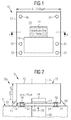
- FIG. 1 shows a bottom view of a semiconductor pressure sensor 10.
- the semiconductor pressure sensor 10 is on a silicon chip 12 arranged of a square base 13 with a Width B of 2.1 mm.
- a thin, pressure-sensitive surface Membrane 14 which has a thickness of 1 ⁇ m, for example.
- On the membrane 14 delimits a circuit area on the base area 13 16 in which components of a detection means have been integrated, which are part of the pressure sensor are.
- In the left edge area of the base 13 there are contact balls 18 to 22 applied.
- In the right margin of the Base area 13 also contains three contact balls 24 to 28. Between the contact balls 18 to 28 and the circuit area 16 run connection lines, not shown.
- the contact balls 18 to 28 are used to connect the Semiconductor pressure sensor to a user circuit. So be a voltage is applied across the contact balls 18 to 28 and Control signals transmitted to the circuit area 16 or Receive signals from circuit area 16.
- the structure of the circuit integrated in the circuit area 16 depends on the pressure detection principle used and on the Requirements for the detection accuracy of the pressure sensor from.
- a capacitive Pressure detection principle used.
- the membrane 14 forms together with the substrate of the chip 12 a plate capacitor with variable pressure capacity.
- an Circuit area 16 integrated current source is this The capacitor is charged and discharged periodically.
- in the Circuit area 16 is also a binary counter unit integrated with each period of the oscillator around the value 1 is increased.
- One lying outside of the pressure sensor 10 Processor of the user circuit causes a control signal the start of the registration process and thus sets the Counter unit to the value zero.
- tM After expiration of one from the processor specified counting interval tM becomes the counting process stopped and the count result can be from the processor via a serial contained in the circuit area 16 Interface can be read out.
- An EEPROM module is also integrated in the circuit area (Electrical Erasable Programmable Read Only Memory), which is used for Storage of calibration data is used and also serial can be described or read. Because of the calibration is an accurate measurement of pressure in a legal way prescribed unit possible, e.g. of air pressure or a water pressure.
- a piezoresistive Pressure detection principle used in the area of the membrane Piezoresistive elements, in which the Carrier mobility and thus the ohmic resistance depending on the ambient pressure or depending on the deflection the membrane changes.
- the means of detection evaluates the Size of the resistor and generates a sensor signal.
- Figure 2 shows a sectional view through the on a Printed circuit board 50 mounted pressure sensor 10 along a in Figure 1 shown sectional area I, which is at an angle of 90 Degree to the drawing plane.
- the pressure sensor 10, the circuit board 50 and the contact balls 18 to 28 form a pressure sensor arrangement 52nd
- FIG. 2 also shows the height h of the semiconductor pressure sensor 10 shown.
- This height h is determined by the height a silicon wafer (wafer) on which the chip 12 made together with other chips of the same structure has been.
- the height h is the same 675 ⁇ m.
- the contact balls 18 to 28 have a diameter of about 175 ⁇ m.
- the membrane 14 borders on a closed one Cavity 54 formed inside the chip 12 is.
- the cavity 54, the membrane 14 and the circuit board 50 are on a line in this order.
- conductor tracks 56 and 58 are also shown, that from the contact ball 18 on the chip 12 to the circuit area 16 lead.
- the circuit board 50 is a conductor track on both sides printed circuit board made of standard FR4 material.
- the component side the circuit board 50 lies on that in FIG. 2 shown page 51, on which the semiconductor pressure sensor 10 is arranged. Between the semiconductor pressure sensor 10 and the circuit board 50 there is a gap 60, the gap width by the diameter of the contact balls 18th to 28 is determined and with the diameter of the contact balls 18 to 28 matches.
- On page 51 of the circuit board 50 are the contact balls 18 and 24 with mating connection surfaces 62 or 64 connected to the connection surfaces the conductor tracks 56 and 58 for connecting the contact balls 18 or 24 are aligned.
- the connection surfaces of the conductor tracks 56 and 58 are in the same position relative to one another, which the mating connection surfaces 62, 64 have each other.
- the pressure sensor 10 was made using the platelet quick assembly technique (Flip chip technology) on the circuit board 50 assembled.
- the contact balls 18 to 28 were first on the connection surfaces of the conductor tracks provided for them 56 to 58 applied. Then the chips isolated by sawing the wafer.
- the isolated chip 12 was with the help of a vacuum pipette 74 on the intended for him Place on the circuit board 50.
- a solder paste was previously in the circuit board 50 a screen printing process. When placing the Contact balls 18 to 28 are pressed into the solder paste. In one following reflow process were the solder paste and edge areas the contact balls 18 to 28 liquefied again, so that Solder connections between the contact balls 18 to 28 and Pads 62, 64 formed on the circuit board 50.
- the circuit board 50 contains one opposite the membrane 14 Area a through hole 66, e.g. a through hole.
- the through hole 66 is used to supply Ambient air to the membrane 14.
- the gap 60 becomes a silicone mass 68 foamed, the through hole remains free of silicone mass 68. Which is in the through hole 66 ambient air presses on the silicone mass 68, which bends due to the pressure and in turn on the membrane 14 presses, see arrow 70.
- the pressure sensor shown in FIGS. 1 and 2 takes up an installation space of approximately 2.1 mm (millimeters) by 2.1 mm by 0.85 mm, ie by 3.8 mm 3 .
- the sensor MS5534AM mentioned in the introduction has a construction volume of 9 mm by 9 mm by 5.2 mm, ie 236 mm 3 .
- the invention thus achieves a reduction in the net volume to approximately 1/60. This volume reduction opens up new areas of application for pressure sensors.
- the chip 12 has a flat and compared to Membrane mechanical robust surface 72 on which a pipette 74 can suck the pressure sensor 10 for assembly.
- the assembly in the context of SMD technology can be very safe and very easy to do.
- the chip 12 was in the exemplary embodiment in CMOS technology (Complementary Metal Oxide Semiconductor). This Technology is characterized by low power consumption made possible by a housing for the To do without chip 12 completely. However, can also other semiconductor technologies for manufacturing the chip 12 deploy.
- CMOS technology Complementary Metal Oxide Semiconductor
- a special surface micromechanical was used to produce the membrane 124 Etching process used. Used for etching Openings in chip 12 were made again after the etching locked.
Landscapes
- Chemical & Material Sciences (AREA)
- Analytical Chemistry (AREA)
- Physics & Mathematics (AREA)
- General Physics & Mathematics (AREA)
- Measuring Fluid Pressure (AREA)
Abstract
Description
- direkt im Schaltungsträger bspw. durch Ausfräsungen,
- in einer auf dem Schaltungsträger aufgetragenen Lotpaste oder Lotstoppaste bspw. durch Weglassen der Paste im Bereich der Kanäle, oder
- in einem Klebstoff mit elektrischen Eigenschaften, die von der Verdichtung des Klebstoffes abhängen, durch Weglassen des Klebstoffes im Bereich der Kanäle.
- Figur 1
- eine Ansicht eines Halbleiter-Drucksensors von unten, und
- Figur 2
- eine Schnittdarstellung durch den auf einer Leiterplatte montierten Halbleiter-Drucksensor.
Claims (12)
- Drucksensoranordnung (52),
mit einer Trägerplatte (12), die eine Membran (14)enthält, die an einen in der Trägerplatte (12) ausgebildeten Hohlraum (54) grenzt,
mit einem von der Membran (14) betätigten und elektronisch arbeitenden Erfassungsmittel (16), das auf der Trägerplatte (12) angeordnet ist,
mit auf der Trägerplatte (12) angeordneten elektrisch leitenden Anschlussflächen (56, 58), die mit dem Erfassungsmittel (16) verbunden sind,
mit einem Schaltungsträger (50), der die Trägerplatte (12), eine Schaltungsanordnung und mit der Schaltungsanordnung elektrisch leitend verbundene Gegenanschlussflächen (62, 64) trägt,
und mit elektrisch leitenden Verbindungselementen (18 bis 28) zwischen den Anschlussflächen (56, 58) und den Gegenanschlussflächen (62, 64),
dadurch gekennzeichnet, dass der Abstand zwischen der Trägerplatte (12) und dem Schaltungsträger (50) durch die Abmessungen der elektrisch leitenden Verbindungselemente (18 bis 28) festgelegt wird,
und dass die Membran (14) zwischen dem Hohlraum (54) und dem Schaltungsträger (50) liegt. - Drucksensoranordnung (52) nach Anspruch 1, dadurch gekennzeichnet, dass zwischen der Trägerplatte (12) und dem Schaltungsträger (50) ein Spalt (60) mit einer Spaltbreite liegt, die kleiner als 1 mm ist.
- Drucksensoranordnung (52) nach einem der vorhergehenden Ansprüche, dadurch gekennzeichnet, dass miteinander verbundene Anschlussflächen (56, 62) und Gegenanschlussflächen (58, 64) jeweils einander zugewandt sind.
- Drucksensoranordnung (52) nach einem der vorhergehenden Ansprüche, dadurch gekennzeichnet, dass eine die Membran (14) enthaltende Fläche (13) der Trägerplatte (12) und die der Membran (14) benachbarte Fläche (51) des Schaltungsträgers (50) parallel zueinander liegen.
- Drucksensoranordnung (52) nach einem der vorhergehenden Ansprüche, dadurch gekennzeichnet, dass die Verbindungselemente (18 bis 28) Lötverbindungen oder elektrisch leitende Klebverbindungen zwischen jeweils einer Anschlussfläche (56, 58) und einer Gegenanschlussfläche (62, 64) sind,
oder dass die Verbindungselemente starre elektrisch leitende Stege sind, deren Enden jeweils an einer Anschlussfläche (56, 58) und an einer Gegenanschlussfläche (62, 64) befestigt sind. - Drucksensoranordnung (52) nach einem der vorhergehenden Ansprüche, dadurch gekennzeichnet, dass der Schaltungsträger (50) und/ oder die Trägerplatte (12) eine Aussparung hat, die zu der Membran (14) führt.
- Drucksensoranordnung (52) nach einem der vorhergehenden Ansprüche, dadurch gekennzeichnet, dass eine durch Umgebungsdruck leicht verformbare Schutzmasse als Schutzschicht (68) zwischen Membran (14) und Schaltungsträger (50) liegt oder als Schutzwand einen Zwischenraum zwischen Membran (14) und Schaltungsträger (50) abdichtet,
und/oder dass die Schutzschicht (68) den Raum (60) zwischen Trägerplatte (12) und Schaltungsträger (50) vollständig ausfüllt. - Drucksensoranordnung (52) nach einem der vorhergehenden Ansprüche, dadurch gekennzeichnet, dass das Erfassungsmittel (16) elektronische Bauelemente enthält, die auf der Trägerplatte (12) integriert sind.
- Drucksensoranordnung (52) nach einem der vorhergehenden Ansprüche, dadurch gekennzeichnet, dass der Schaltungsträger (50) eine flexible Leiterfolie oder eine Leiterplatte ist, die mindestens eine Leiterschicht und mindestens eine Isolierschicht enthält.
- Drucksensoranordnung (52) nach einem der vorhergehenden Ansprüche, dadurch gekennzeichnet, dass die Anschlussflächen (56, 58) auf der die Membran (14) enthaltenden Fläche (13) der Trägerplatte (12) angeordnet sind.
- Herstellungsverfahren für eine Drucksensoranordnung (52),
bei dem eine Trägerplatte (12) gefertigt wird, die eine Membran (14)enthält,
bei dem die Trägerplatte (12) mit elektrisch leitenden Verbindungselementen (18 bis 28) versehen wird,
bei dem die Trägerplatte (12) an einen Schaltungsträger (50) in einem durch die Verbindungselemente festgelegten Abstand angeordnet wird, wobei diejenige Seite der Trägerplatte, welche die Membran trägt, dem Schaltungsträger (50) zugewandt ist,
und bei dem die Verbindungselemente (18 bis 28) anschließend mit elektrisch leitenden Anschlussflächen (62, 64) elektrisch leitend verbunden werden, die auf dem Schaltungsträger (50) an den Enden der Verbindungselemente (18 bis 28) angeordnet sind. - Herstellungsverfahren nach Anspruch 11, dadurch gekennzeichnet, dass beim Herstellungsverfahren Verfahrensschritte ausgeführt werden, die zum Herstellen einer Drucksensoranordnung (52) nach einem der Ansprüche 1 bis 10 erforderlich sind.
Applications Claiming Priority (2)
| Application Number | Priority Date | Filing Date | Title |
|---|---|---|---|
| DE10134847A DE10134847A1 (de) | 2001-07-17 | 2001-07-17 | Drucksensoranordnung und zugehöriges Herstellungsverfahren |
| DE10134847 | 2001-07-17 |
Publications (1)
| Publication Number | Publication Date |
|---|---|
| EP1278053A1 true EP1278053A1 (de) | 2003-01-22 |
Family
ID=7692156
Family Applications (1)
| Application Number | Title | Priority Date | Filing Date |
|---|---|---|---|
| EP02102021A Withdrawn EP1278053A1 (de) | 2001-07-17 | 2002-07-11 | Drucksensoranordnung und zugehöriges Herstellungsverfahren |
Country Status (2)
| Country | Link |
|---|---|
| EP (1) | EP1278053A1 (de) |
| DE (1) | DE10134847A1 (de) |
Cited By (2)
| Publication number | Priority date | Publication date | Assignee | Title |
|---|---|---|---|---|
| WO2006045653A1 (de) * | 2004-10-22 | 2006-05-04 | Robert Bosch Gmbh | Verfahren zum montieren von halbleiterchips und entsprechende halbleiterchipanordnung |
| EP1800101B1 (de) * | 2004-07-02 | 2016-04-20 | Honeywell International Inc. | Auspuff-rückdrucksensor mit einem absoluten mikrobearbeiteten druckmesschip und herstellungsverfahren dafür |
Citations (3)
| Publication number | Priority date | Publication date | Assignee | Title |
|---|---|---|---|---|
| US5856914A (en) * | 1996-07-29 | 1999-01-05 | National Semiconductor Corporation | Micro-electronic assembly including a flip-chip mounted micro-device and method |
| EP0951069A1 (de) * | 1998-04-17 | 1999-10-20 | Interuniversitair Microelektronica Centrum Vzw | Herstellungsverfahren für eine Mikrostruktur mit Innenraum |
| US6178249B1 (en) * | 1998-06-18 | 2001-01-23 | Nokia Mobile Phones Limited | Attachment of a micromechanical microphone |
-
2001
- 2001-07-17 DE DE10134847A patent/DE10134847A1/de not_active Withdrawn
-
2002
- 2002-07-11 EP EP02102021A patent/EP1278053A1/de not_active Withdrawn
Patent Citations (3)
| Publication number | Priority date | Publication date | Assignee | Title |
|---|---|---|---|---|
| US5856914A (en) * | 1996-07-29 | 1999-01-05 | National Semiconductor Corporation | Micro-electronic assembly including a flip-chip mounted micro-device and method |
| EP0951069A1 (de) * | 1998-04-17 | 1999-10-20 | Interuniversitair Microelektronica Centrum Vzw | Herstellungsverfahren für eine Mikrostruktur mit Innenraum |
| US6178249B1 (en) * | 1998-06-18 | 2001-01-23 | Nokia Mobile Phones Limited | Attachment of a micromechanical microphone |
Cited By (4)
| Publication number | Priority date | Publication date | Assignee | Title |
|---|---|---|---|---|
| EP1800101B1 (de) * | 2004-07-02 | 2016-04-20 | Honeywell International Inc. | Auspuff-rückdrucksensor mit einem absoluten mikrobearbeiteten druckmesschip und herstellungsverfahren dafür |
| WO2006045653A1 (de) * | 2004-10-22 | 2006-05-04 | Robert Bosch Gmbh | Verfahren zum montieren von halbleiterchips und entsprechende halbleiterchipanordnung |
| US7563634B2 (en) | 2004-10-22 | 2009-07-21 | Robert Bosch Gmbh | Method for mounting semiconductor chips, and corresponding semiconductor chip system |
| CN100584741C (zh) * | 2004-10-22 | 2010-01-27 | 罗伯特·博世有限公司 | 用于装配半导体芯片的方法及相应的半导体芯片装置 |
Also Published As
| Publication number | Publication date |
|---|---|
| DE10134847A1 (de) | 2003-02-06 |
Similar Documents
| Publication | Publication Date | Title |
|---|---|---|
| DE102016213878B3 (de) | Gehäuse für einen Mikrochip mit einem strukturierten Schichtverbund und Herstellungsverfahren dafür | |
| DE3347848C2 (de) | ||
| DE69015766T2 (de) | Kapazitiver Beschleunigungsmesser. | |
| DE19730914B4 (de) | Mikroelektronik-Baugruppe | |
| DE4423893C2 (de) | Flachdichtung mit flexibler Leiterplatte | |
| EP1046030B1 (de) | Anordnung zur feuchtemessung | |
| DE69416571T2 (de) | Beschleunigungsmessaufnehmer | |
| DE102010002545A1 (de) | Sensorvorrichtung und Herstellverfahren für eine Sensorvorrichtung | |
| EP1078330A1 (de) | Sensoreinrichtung zur erfassung von biometrischen merkmalen, insbesondere fingerminutien | |
| EP1393605B1 (de) | Leiterplatte mit mindestens einem elektronischen bauteil | |
| WO2001086588A1 (de) | Chipkarte | |
| DE19808986A1 (de) | Halbleiterbauelement mit mehreren Halbleiterchips | |
| EP3111474B1 (de) | Verfahren zum herstellen einer leiterplatte mit eingebettetem sensorchip sowie leiterplatte | |
| DE10134847A1 (de) | Drucksensoranordnung und zugehöriges Herstellungsverfahren | |
| EP1049362B1 (de) | Leiterplatte mit wärmeleitendem Bereich | |
| EP1897423A1 (de) | Sensor für einen hardwareschutz für sensible elektronik-datenbaugruppen gegen externe manipulationen | |
| DE102011118734A1 (de) | Verbundlagenschaltung mit von aussen zugänglichen integrierten Komponenten | |
| EP1804557A1 (de) | Elektronik-Sicherheits-Modul | |
| DE19902450A1 (de) | Miniaturisiertes elektronisches System und zu dessen Herstellung geeignetes Verfahren | |
| EP2340693A1 (de) | Elektrische schaltungsanordnung sowie verfahren zum herstellen einer elektrischen schaltungsanordnung | |
| DE102005062799A1 (de) | Elektronik-Sicherheits-Modul | |
| EP3263471B1 (de) | Etikettensensor zum abtasten von etiketten auf einem trägerband | |
| DE19830540A1 (de) | Elektronischer Schaltungsträger | |
| DE102020102493A1 (de) | Die mit Gehäuse und Montageverfahren | |
| DE4224103A1 (de) | Miniaturgehäuse mit elektronischen Bauelementen |
Legal Events
| Date | Code | Title | Description |
|---|---|---|---|
| PUAI | Public reference made under article 153(3) epc to a published international application that has entered the european phase |
Free format text: ORIGINAL CODE: 0009012 |
|
| AK | Designated contracting states |
Kind code of ref document: A1 Designated state(s): AT BE BG CH CY CZ DE DK EE ES FI FR GB GR IE IT LI LU MC NL PT SE SK TR |
|
| AX | Request for extension of the european patent |
Free format text: AL;LT;LV;MK;RO;SI |
|
| 17P | Request for examination filed |
Effective date: 20030722 |
|
| AKX | Designation fees paid |
Designated state(s): DE FR GB IT |
|
| RAP1 | Party data changed (applicant data changed or rights of an application transferred) |
Owner name: BENQ MOBILE GMBH & CO. OHG |
|
| 17Q | First examination report despatched |
Effective date: 20061228 |
|
| 19U | Interruption of proceedings before grant |
Effective date: 20070101 |
|
| 19W | Proceedings resumed before grant after interruption of proceedings |
Effective date: 20070702 |
|
| 19W | Proceedings resumed before grant after interruption of proceedings |
Effective date: 20090803 |
|
| RAP1 | Party data changed (applicant data changed or rights of an application transferred) |
Owner name: PALM, INC. |
|
| R17C | First examination report despatched (corrected) |
Effective date: 20090803 |
|
| RAP1 | Party data changed (applicant data changed or rights of an application transferred) |
Owner name: HEWLETT-PACKARD DEVELOPMENT COMPANY, L.P. |
|
| GRAP | Despatch of communication of intention to grant a patent |
Free format text: ORIGINAL CODE: EPIDOSNIGR1 |
|
| INTG | Intention to grant announced |
Effective date: 20140304 |
|
| RAP1 | Party data changed (applicant data changed or rights of an application transferred) |
Owner name: QUALCOMM INCORPORATED |
|
| STAA | Information on the status of an ep patent application or granted ep patent |
Free format text: STATUS: THE APPLICATION IS DEEMED TO BE WITHDRAWN |
|
| 18D | Application deemed to be withdrawn |
Effective date: 20140715 |