EP1276144B1 - A method and apparatus for detecting breakdown in ultra thin dielectric layers. - Google Patents
A method and apparatus for detecting breakdown in ultra thin dielectric layers. Download PDFInfo
- Publication number
- EP1276144B1 EP1276144B1 EP02447071.8A EP02447071A EP1276144B1 EP 1276144 B1 EP1276144 B1 EP 1276144B1 EP 02447071 A EP02447071 A EP 02447071A EP 1276144 B1 EP1276144 B1 EP 1276144B1
- Authority
- EP
- European Patent Office
- Prior art keywords
- readings
- values
- breakdown
- current
- ref
- Prior art date
- Legal status (The legal status is an assumption and is not a legal conclusion. Google has not performed a legal analysis and makes no representation as to the accuracy of the status listed.)
- Expired - Lifetime
Links
Images


Classifications
-
- H—ELECTRICITY
- H10—SEMICONDUCTOR DEVICES; ELECTRIC SOLID-STATE DEVICES NOT OTHERWISE PROVIDED FOR
- H10P—GENERIC PROCESSES OR APPARATUS FOR THE MANUFACTURE OR TREATMENT OF DEVICES COVERED BY CLASS H10
- H10P74/00—Testing or measuring during manufacture or treatment of wafers, substrates or devices
- H10P74/20—Testing or measuring during manufacture or treatment of wafers, substrates or devices characterised by the properties tested or measured, e.g. structural or electrical properties
- H10P74/203—Structural properties, e.g. testing or measuring thicknesses, line widths, warpage, bond strengths or physical defects
Definitions
- Oxide breakdown is one of the most threatening failure mechanisms in integrated circuits. As the oxide thickness is decreased in the sub-5nm range, the breakdown definition itself is no longer clear and its detection becomes problematic.
- the present invention is related to methods of detecting the breakdown in dielectric layers, in particular oxide layers of such low thickness.
- SBD is usually associated with a smaller current jump during a Constant Voltage Stress (CVS) or a smaller voltage drop during Constant Current Stress (CCS) compared to the HBD case.
- CVS Constant Voltage Stress
- CCS Constant Current Stress
- the soft and hard breakdowns are caused by the same physical mechanism: SBD is considered to be a breakdown without the thermal runaway effects that lead to a low-resistance breakdown path connecting gate and substrate [1].
- SBD occurs when the generated density of traps during a CVS or CCS has sufficiently increased to generate (at some random place on the capacitor area) a breakdown path of traps connecting anode with cathode.
- SBD is (just as HBD) a local event.
- Ig-Vg characteristic of the SBD is, apart from some statistical fluctuations, independent of the test area [3].
- This IV-curve is the most unambiguous signature of an SBD event, and measuring it is therefore the most direct way to detect SBD.
- this approach has the disadvantage that the stress needs to be interrupted at regular time intervals to measure the low voltage current. This is time-consuming and might influence the time-to-breakdown, especially when the current or voltage overshoot at the start of each stress interval is not well-controlled.
- US 5804975 discloses the detection of the breakdown of an ultra-thin dielectric layer by applying a test signal to the layer. Measurements are taken of noise signals present in the layer during the application of the test signal. At breakdown, a significant increase occurs in the amplitude of the measured noise signals.
- the present invention aims to provide a accurate method for detecting soft breakdown events in integrated circuit devices, wherein a reduced sensitivity is present to pre-breakdown events, resulting in a lower probability of erroneous breakdown detection.
- the present invention is related to a method for detecting breakdown in a dielectric layer, comprising the steps of:
- the value of said one selected reading is the median (m r ) of the values of said set of readings.
- a second set of readings is measured, said second set consisting of at least twice the amount of readings of said first set of readings, and wherein said reference value is a function of the value of a selected reading of said second set, said selected reading being selected in the same way as said selected reading of said first set.
- the value of said selected reading of said second set is the median (m ref ) of the values of said second set of readings.
- the sorting of said sets of readings is preferably done according to an indirect insertion sorting technique.
- said signal is a voltage signal, corresponding to a voltage difference across said layer, and said readings are absolute values of the change of the current flowing through said layer, as a consequence of said voltage signal, said change being calculated on the basis of a set of current readings, as the difference between two subsequent current readings of said set.
- said signal is a current signal, corresponding to a current flowing through said layer, and said readings are absolute values of the change of the voltage across said layer, as a consequence of said current signal, said change being calculated on the basis of a set of voltage readings, as the difference between two subsequent voltage readings of said set.
- an apparatus for detecting breakdown in a dielectric layer comprising:
- said means for comparing comprises means for sorting said sets of readings according to an indirect insertion sorting technique.
- said test signal may be a voltage signal, corresponding to a voltage difference across said layer, in which case said readings are absolute values of current changes.
- said test signal may be a current signal, corresponding to a current through said layer, in which case said readings are absolute values of voltage changes.
- the present invention is related to a new optimized trigger algorithm for SBD based on gate current noise increase that is sufficiently reliable to be applied for real-time, automatic BD detection. Automated BD tests often stress the devices till HBD occurs. The method according to the invention even allows interruption of the CVS upon detection of SBD, resulting in considerably shorter overall test times.
- the current vs. time behaviour in small dimension transistors during a Constant Voltage Stress shows RTS-like events 2 as illustrated in fig. 1 .
- These gate current jumps are not breakdowns, but pre-breakdown events because the t BD -distributions obtained on two different areas by triggering on these jumps do not line up after the well-known area scaling law has been applied.
- a 5 percent step trigger is needed to approximate the noise-triggered distribution. Only the noise-triggered distributions line up for both areas, proving that the gate current steps observed in small area devices are not breakdowns, but pre-breakdown events.
- the simplest approach to applying noise for breakdown detection is monitoring the sample standard deviation of a number of gate current values, preferably in a subset containing a fixed number n r of consecutive current measurements including the last measured value.
- the set should be chosen sufficiently large to generate statistically relevant parameters, but it should still be sufficiently small to allow for an acceptable time resolution.
- the 'running' estimate s' for the standard deviation ⁇ will increase when the gate current noise increases at breakdown.
- the present invention solves this problem in an elegant way by selecting a value of the ⁇ set which is not an outlier value, as the breakdown monitor.
- An outlier value can then be defined as a value which is significantly higher or lower than the majority of values in the set.
- outlier values are identified by the fact that they exceed a predefined border value, such 10 -9 A in the example above.
- the selected value is the median m r of the ⁇ set.
- finding the median of a dataset consists of sorting the data and taking the middle value as the central value estimator, see the vertical arrows above each set of ⁇ I-values.
- the average of the middle two values is taken. This complication can be avoided by requiring an odd number of ⁇ values.
- curve 23 shows the evolution of m r as a function of time. m r is not increased by the gate current peak, which introduces only one high ⁇ I-value in the set, which in turn does not affect the running median m r .
- a running reference value is constructed along with the running non-outlier value, preferably the median m r .
- the running reference is constructed in an identical way as m r , but it is based on n ref current values, with n ref >2 ⁇ n r .
- a second set of n ref -1 current changes is calculated on the basis of the n ref current values, and the running reference is selected as a non-outlier value of said second set.
- the running reference is the median m ref of said second set. Breakdown is triggered when a significant difference between m ref and m r is detected, or equivalently, when the ratio m r /m ref exceeds a given value 'a'.
- the median m r is compared to a reference value which is a linear function a.m ref , of the reference median m ref .
- a.m ref a linear function of the reference median m ref .
- this test simply reduces to finding when the square root of the F-ratio exceeds a fixed detection threshold which can be calculated before the stress measurement starts.
- a default 99.73% value for the significance probability is preferably chosen, as this corresponds with the 3 ⁇ limits for a normally distributed signal, which is commonly used for statistical process control purposes.
- Fig. 6A shows the current increase due to SBD.
- Curves 30 and 31 represent the m r and m ref values, as a function of time.
- the m r -curve 30 shows a rather gradual increase, making it difficult for a simple step detecting algorithm to trigger properly.
- Fig. 6C shows the evolution of the ratio m r /m ref .
- the real-time detection algorithm has to be designed in a computationally efficient way, so that it can keep up with the stream of incoming current values from the measurement hardware. Performing a complete sort of each range subset upon acquisition of a new current value would take a considerable amount of the computation time needed by the algorithm. It is more efficient to perform an indirect insertion sort (see also reference [6]) "on the fly" on an array of moving range values stored in a cyclic way. Indirect sorting reorders an array of indices to the data points instead of the data points themselves.
- the m r /m ref ratio detection level determines the detection efficiency of the algorithm: for Gaussian noise, a higher m r /m ref ratio lowers the ⁇ risk (representing the probability of false early detections) at the expense of a higher ⁇ risk (representing the probability of overlooking a true noise increase due to SBD). A proper balance between these two risks should be determined for a given measurement setup by means of a calibration procedure.
- n r and n ref values enhance the distinctive power of the detection algorithm: both the ⁇ risk and the ⁇ risk are predictably lower for Gaussian noise.
- increasing n r and n ref also enhances the robustness of the algorithm against "non-Normal" events like spikes, pre-BD steps, and more specifically, longer RTS-like signals, as a larger amount of outlier ranges have to accumulate in the sorted moving range statistic before they reach its middle.
- using larger n r and n ref values for detection is at the expense of a lower time resolution for the t BD values: as half of the short range sample collection time is taken as the average delay time for detection, longer samples correspond with a larger uncertainty on t BD .
- the 3D surface plot in fig. 7 shows an experimental verification of the algorithm efficiency as a function of n r and the m r /m ref -ratio detection level.
- the t BD times (either SBD or HBD) of a set of NMOS transistors with 2.4 nm gate oxide thickness stressed in inversion at 4.4V were determined through visual inspection of the I(t) curves measured till HBD. Some I(t) curves showing a slow gradual increase of the noise were discarded from the original dataset, as it was too hard to unambiguously pinpoint the SBD time on them. Note that once the SBD detection algorithm according to the invention is tuned properly, it can be used to determine the SBD time for the "problem" I(t) curves as well.
- the percentage of false detections were then plotted as a function of n r and m r /m ref ( fig. 7 ) .
- n r and m r /m ref values lead to an extremely high percentage of false early SBD detections (above 50%). In this region of the plot, the experimental ⁇ risk dominates.
- higher n r and m r /m ref values lead to a relatively high percentage of late detections (above 5%): the experimental ⁇ risk dominates in that region of the plot.
- Fig. 9 shows the detection margin for a 1 mm 2 capacitor as a function of the stress voltage.
- the background noise of the measurement system must be smaller than the signature noise attributed to SBD.
- the resolution of the current meter must be such that it is capable of measuring the noise before breakdown.
- Digital current meters return quantised current levels when the true current fluctuations are close to their resolution limit, resulting in occasional zero m ref values.
- the algorithm can be protected against this by replacing any of the corresponding zero ⁇ ref values with the user-specified ⁇ ref value, if occurring.
- the voltage source compliance setting can be used as a separate trigger for HBD.
- some voltage sources return a constant measured current value when in compliance. The noise detection algorithm cannot be used for detection of the HBD event then, so that this separate HBD trigger is even mandatory for such configurations.
- the present invention is related to an accurate and robust triggering algorithm for soft breakdown based on gate current noise increase that is sufficiently reliable to be applied for real-time, automatic BD detection, with acceptable execution speed if implemented properly. Triggering on current spikes or pre-BD events is avoided. This test assures correct SBD-detection in a wide range of stress conditions and various geometries. The efficiency of the algorithm and the influence of its parameters have been discussed.
- Appendix 1 The median moving range as a robust sigma estimator
- This appendix explains how the concept of a robust ⁇ estimator originates from Statistical Process Control (SPC) and derives the relationship between the median moving range and the corresponding sigma predictor for a Normally distributed signal.
- SPC Statistical Process Control
- a process In a production environment, a process is under control when the variation of a chosen output parameter is within a given required tolerance.
- the capability of a process is defined as the ratio between this tolerance and the lowest achievable output variation.
- Statistical process control is the method of choice to assess this capability, and to timely detect significant deviations from the target output.
- the mean moving range E(r) of a process characteristic signal is often used to predict its short term variation.
- the historical data used for that purpose often show slow process drifts, so that the historical sample standard deviation s' becomes significantly larger than the true short term random deviation ⁇ reflecting the process capability.
- the mean moving range filters out most of the signal drift, if occurring.
- a sufficient amount of historical data is needed to reliably predict the true population ⁇ value using a predictor based on the mean moving range.
- a sufficiently long process characteristic even shows sudden shifts caused by input parameter adjustments (e.g. to correct for a known drift due to machine wearout). Such shifts show up as outliers in the moving range statistic.
- the mean moving range is linearly sensitive to outliers, so that a ⁇ predictor based on it can become artificially larger and cause an underestimation of the process capability.
- steps and RTS-like signals can also be seen as sudden shifts of the characteristic signal.
- the median moving range m r even filters out such outliers, so that a ⁇ predictor based on it will be more robust against that type of non-Normality of the signal.
- the proof is based on the properties of a Poisson process.
- the moving range statistic (with a subgroup size of 2) consists of taking the absolute value of those differences, thus mirroring the left side of the density function to the right. Due to the symmetry of the density function, this simply doubles the part to the right of the vertical axis.
- This appendix shows how the execution time of the algorithm can be reduced considerably by using indirect insertion sorting for the real-time computation of both median moving range values.
- This approach even allows to store only a single array of (n ref -1) range values in memory and to perform the indirect insertion sort for both m r and m ref using 2 arrays of indices to that same ⁇ subset.
- the index array Sh_rng_indx is filled. Because the indices are uniquely defined, it is possible to continue as follows:
Landscapes
- Testing Or Measuring Of Semiconductors Or The Like (AREA)
- Testing Of Individual Semiconductor Devices (AREA)
- Testing Relating To Insulation (AREA)
Description
- Oxide breakdown is one of the most threatening failure mechanisms in integrated circuits. As the oxide thickness is decreased in the sub-5nm range, the breakdown definition itself is no longer clear and its detection becomes problematic. The present invention is related to methods of detecting the breakdown in dielectric layers, in particular oxide layers of such low thickness.
- The following documents belonging to the state of the art are referred to in this section:
- [1] "Soft breakdown of ultra-thin gate oxide layers", M. Depas, T. Nigam et al. IEEE Trans. Elec. Dev., vol. 43, no. 9, pp. 1499-1504, 1996.
- [2] "Structural dependence of Dielectric breakdown in ultra-thin gate oxides and its relationship to soft breakdown modes and device failure", E.Y. Wu et al. IEDM Tech. Dig., pp. 187-190, 1998.
- [3] "On the properties of the gate and substrate current after softbreakdown in ultrathin oxide layers", F. Crupi, R. Degraeve et al. IEEE Trans. Elec. Dev., vol. 45, no. 11, pp. 2329-2334, 1998.
- [4] "Ultra-thin gate dielectrics : they break down, but do they fail ?", B. Weir et al. , IEDM Tech. Dig, pp. 73-76, 1997.
- [5] "Trap assisted tunneling as a mechanism of degradation and noise in 2-5nm oxides", G.B. Alers et al., IRPS Proc., pp.76-79, 1998.
- [6] S. Baase, Computer Algorithms. New York: Addison-Wesley, 1988, ch. 2, pp. 47-52.
- An accurate determination of the gate oxide reliability is of the utmost importance for the correct prediction of IC lifetime. In the past, the accuracy of this prediction was mainly limited by the accuracy of the extrapolation from high voltage time-to-breakdown (tBD) data to low voltage. Apart from the distinction between intrinsic and extrinsic breakdown, the intrinsic mode can be 'soft' or 'hard' [1]. Since the identification of soft and hard breakdown modes (SBD and HBD, respectively), the definitions of oxide breakdown and oxide failure are no longer obvious. Defining soft breakdown (SBD) and hard breakdown (HBD) precisely turns out to be a difficult task. SBD is usually associated with a smaller current jump during a Constant Voltage Stress (CVS) or a smaller voltage drop during Constant Current Stress (CCS) compared to the HBD case. As confirmed by some research groups, the soft and hard breakdowns are caused by the same physical mechanism: SBD is considered to be a breakdown without the thermal runaway effects that lead to a low-resistance breakdown path connecting gate and substrate [1]. Based on this assumption and the observation that hard breakdown is dominant in small geometry transistors [2], we consider the time-to-first breakdown, regardless whether it is soft or hard, as time-to-breakdown in this description.
- This leaves us with the problem of correctly determining the time-to-soft breakdown. SBD occurs when the generated density of traps during a CVS or CCS has sufficiently increased to generate (at some random place on the capacitor area) a breakdown path of traps connecting anode with cathode. SBD is (just as HBD) a local event. As a consequence the Ig-Vg characteristic of the SBD is, apart from some statistical fluctuations, independent of the test area [3]. This IV-curve is the most unambiguous signature of an SBD event, and measuring it is therefore the most direct way to detect SBD. However, this approach has the disadvantage that the stress needs to be interrupted at regular time intervals to measure the low voltage current. This is time-consuming and might influence the time-to-breakdown, especially when the current or voltage overshoot at the start of each stress interval is not well-controlled.
- A more elegant method is to determine the breakdown event real-time by monitoring the most adequate parameter. In [4,5], it has been observed that SBD is accompanied by a gate current noise increase. This increase has been used as a trigger for SBD detection [5].
- However, simple noise monitors like the variance of current values during constant voltage stress are too sensitive to pre-BD events and spikes, resulting in false BD triggers.
-
US 5804975 discloses the detection of the breakdown of an ultra-thin dielectric layer by applying a test signal to the layer. Measurements are taken of noise signals present in the layer during the application of the test signal. At breakdown, a significant increase occurs in the amplitude of the measured noise signals. - The present invention aims to provide a accurate method for detecting soft breakdown events in integrated circuit devices, wherein a reduced sensitivity is present to pre-breakdown events, resulting in a lower probability of erroneous breakdown detection.
- The present invention is related to a method for detecting breakdown in a dielectric layer, comprising the steps of:
- applying a signal to said dielectric layer,
- measuring a plurality of sets of readings having values, which are in relation to said signal,
- searching and identifying outlier readings in each of said sets, said outlier readings being defined by the fact that they have values which are significantly higher or lower than the majority of the values of said set,
- selecting from each of said sets, one reading which is not one of said outlier readings,
- comparing the value of said one selected reading to a reference value, so that the exceeding of said value leads to the conclusion that a predefined probability is present for having a breakdown state in said layer.
- Preferably, the value of said one selected reading is the median (mr) of the values of said set of readings.
- In the method of the present invention, for each set of readings, a second set of readings is measured, said second set consisting of at least twice the amount of readings of said first set of readings, and wherein said reference value is a function of the value of a selected reading of said second set, said selected reading being selected in the same way as said selected reading of said first set.
- The value of said selected reading of said second set is the median (mref) of the values of said second set of readings.
- Said function is a linear function f(mref) = amref, with a predefined factor 'a'.
- In the method of the invention, the sorting of said sets of readings is preferably done according to an indirect insertion sorting technique.
- According to a first embodiment, said signal is a voltage signal, corresponding to a voltage difference across said layer, and said readings are absolute values of the change of the current flowing through said layer, as a consequence of said voltage signal, said change being calculated on the basis of a set of current readings, as the difference between two subsequent current readings of said set.
- According to a second embodiment, said signal is a current signal, corresponding to a current flowing through said layer, and said readings are absolute values of the change of the voltage across said layer, as a consequence of said current signal, said change being calculated on the basis of a set of voltage readings, as the difference between two subsequent voltage readings of said set.
- According to an aspect not being part of the invention it is disclosed an apparatus for detecting breakdown in a dielectric layer, said apparatus comprising:
- means for applying a test signal to a dielectric layer,
- means for measuring a number of sets of readings,
- means for searching and selecting one reading in each set,
- means for comparing the value of said one selected reading to a reference value,
- output means for indicating that a breakdown state is present in said layer, with a given probability, on the basis of said comparison.
- According to an embodiment not according to the invention, said means for comparing comprises means for sorting said sets of readings according to an indirect insertion sorting technique.
- In an apparatus not according to the invention, said test signal may be a voltage signal, corresponding to a voltage difference across said layer, in which case said readings are absolute values of current changes.
- Alternatively, in an apparatus not according to the invention, said test signal may be a current signal, corresponding to a current through said layer, in which case said readings are absolute values of voltage changes.
-
-
Figure 1 illustrates the gate current of an NMOS transistor as a function of time, until breakdown occurs. -
Figure 2 represents the Weibull distributions of time-to-breakdown for a small and large device, for different trigger methodologies. -
Figure 3 illustrates the relation between the detection level and the current increase upon breakdown. -
Figure 4 illustrates the capability of different noise estimators to avoid false breakdown detection. -
Figure 5 illustrates the capability of the method of the invention to detect an actual breakdown event. -
Figure 6 illustrates the detection of breakdown with the help of a running reference value for the noise estimator. -
Figure 7 gives an overview of the influence of several parameters on the accuracy of the detection algorithm. -
Figure 8 is showing the relation between the detection capabilities of the method of invention, and the capacitor area involved. -
Figure 9 is showing the same relation asfigure 8 , but for small devices only. -
Figure 10 illustrates problems that may arise in the case of long RTS-like signals. - The present invention is related to a new optimized trigger algorithm for SBD based on gate current noise increase that is sufficiently reliable to be applied for real-time, automatic BD detection. Automated BD tests often stress the devices till HBD occurs. The method according to the invention even allows interruption of the CVS upon detection of SBD, resulting in considerably shorter overall test times.
- In the next section, the need for a reliable SBD detection algorithm for automatic CVS measurements on ultra thin oxides is demonstrated. Then, the new noise-based SBD detection algorithm of the invention is presented, with specific attention for some real-time implementation issues. Next, the sensitivity of the algorithm as a function of its input parameters is studied. Finally, the influence of capacitor area, stress voltage, Random Telegraph Signal-like (RTS) pre-BD events, early breakdowns and the measurement hardware are discussed.
- The following description will focus on NMOS transistors with small dimensions, stressed in inversion, because this condition mimics the real situation in circuits, and because the high voltage stressing of very thin oxides becomes inaccurate in large area devices due to parasitic series resistance. However, the present invention is not restricted to NMOS transistors. The description further focuses on gate current measurement during CVS. However, the method of the invention is valid also for voltage measurements during CCS. It will suffice to replace every reference to current values Ig or relative current values ΔI in the following description by analogue voltage values Vg and ΔV.
-
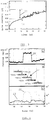
Figure 1 shows the current vs. time behaviour untilbreakdown 1 for an NMOS transistor of dimensions (length X width) 0.2 X 10 µm2, stressed under Vg = 4.4V. The current vs. time behaviour in small dimension transistors during a Constant Voltage Stress shows RTS-like events 2 as illustrated infig. 1 . These gate current jumps are not breakdowns, but pre-breakdown events because the tBD-distributions obtained on two different areas by triggering on these jumps do not line up after the well-known area scaling law has been applied.Figure 2 shows the Weibull plot of the area scaled tBD-distribution (scaled to 2X10⁻⁸ cm2 - oxide thickness = 2.4nm), measured by triggering on noise increase, or by triggering on a gate current step of 1, 2 or 5 percent, in the case of a small area of 2X10⁻⁸ cm2 (group of curves 10) and in the case of a larger area of 2X10⁻⁶ cm2 (group of curves 11) .
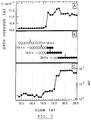
In small area devices, a 5 percent step trigger is needed to approximate the noise-triggered distribution. Only the noise-triggered distributions line up for both areas, proving that the gate current steps observed in small area devices are not breakdowns, but pre-breakdown events. - It should be noted that when pre-BD is mistaken for real breakdown, a flatter tBD-distribution is obtained which will lead to erroneous prediction of the oxide reliability. Also, after each pre-BD gate current step no significant noise increase is measured which confirms that noise is a well-suited monitor for detecting soft breakdown. Only when the detection sensitivity for current steps is lowered, triggering on pre-BD events in small devices is avoided, but applying the same sensitivity to larger areas leads to several SBD's being overlooked. This is illustrated in
figure 3 , which is relative to an NMOS transistor of size (length X width) 1X100µm2, stressed at Vg=4.4V. Atpoint 12, SBD occurs, which would not be detected by a 5% step trigger 13. - The simplest approach to applying noise for breakdown detection is monitoring the sample standard deviation of a number of gate current values, preferably in a subset containing a fixed number nr of consecutive current measurements including the last measured value. The set should be chosen sufficiently large to generate statistically relevant parameters, but it should still be sufficiently small to allow for an acceptable time resolution. The 'running' estimate s' for the standard deviation σ will increase when the gate current noise increases at breakdown.
- It is also possible to consider a set with nr absolute values of consecutive current changes ΔI, wherein ΔI=|In-In-1|. The mean moving range E(r) is the average of this Δ set and also represents a simple monitor for the noise on the current signal. It can be mathematically proven that the predicted value of this running mean E(r) is proportional to the σ of the currents for normally distributed current fluctuations. Mathematical proof of this is given in
Appendix 1. - Both monitors defined above have one major disadvantage: they are sensitive to current steps (such as pre-BD events) and current spikes (caused by accidental measurement errors), resulting in false triggers: a large outlier Δ will heavily influence the sum of Δ values used for computation of the mean moving range E(r), while a single outlier current in the subset will even completely dominate the sum of squares for the computation of s'.
Figure 4 illustrates this problem. The figure is valid for an NMOS transistor of 0.2X10µm2, stressed at Vg=4.4V.Fig. 4A shows a gatecurrent jump 20 as a function of time, which is not related to a breakdown phenomenon, and should not be detected as such by the noise-based algorithm.figure 4B illustrates a series ofsets 21 of 11 measured ΔI-values ranked from low to high, each ΔI-value based on the measurement of nr=12 gate current (Ig) values. Open circles correspond to ΔI-values below 10-9 A; black circles correspond to ΔI-values above 10-9 A. Each set containing one slope of the current jump therefore comprises one black circle. If the running standard deviation s' is to be used (based on the current values Ig themselves, not the ΔI-values), the result, as a function of time, is visible infigure 4C , see the dottedlines 22. It is clear that the running standard deviation s' increases by afactor 10 due to this current jump, which would result in a false trigger. - The present invention solves this problem in an elegant way by selecting a value of the Δ set which is not an outlier value, as the breakdown monitor. An outlier value can then be defined as a value which is significantly higher or lower than the majority of values in the set. Preferably, outlier values are identified by the fact that they exceed a predefined border value, such 10-9 A in the example above.
- Preferably, the selected value is the median mr of the Δ set. For an odd number of values, finding the median of a dataset consists of sorting the data and taking the middle value as the central value estimator, see the vertical arrows above each set of ΔI-values. For an even number of values, the average of the middle two values is taken. This complication can be avoided by requiring an odd number of Δ values. The effect is illustrated in
figure 4C ,curve 23, which shows the evolution of mr as a function of time. mr is not increased by the gate current peak, which introduces only one high ΔI-value in the set, which in turn does not affect the running median mr. - The predicted value of this running median mr is also proportional to the σ of the currents for normally distributed current fluctuations, but the proportionality factor is different (proof equally given in Appendix 1) due to the skewness of the range distribution. In
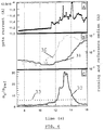
figure 5 , it is illustrated why the median will trigger correctly in the case of soft breakdown.Figure 5 is relative to an NMOS transistor or 1 X 100µm2 stressed at Vg=4.4V.Fig. 5A shows the gate current increase due to SBD.Fig. 5B shows consecutive sets of ΔI-values, whileFig. 5C shows the running median mr, as a function of time. Effectively, mr increases when SBD occurs. On the basis offigs. 4 and5 , one can conclude that the 'running median' triggers correctly on soft breakdown, but is insensitive to single current jumps and spikes, as large outlier Δ values are sorted to the upper end of the range statistic. For this reason, mr is called a robust estimator of σ. - With this breakdown monitor established, an obvious detection algorithm would look for steps of mr as a function of stress time. However, the noise increase is not always very abrupt, as illustrated in
fig. 6 . A point-by-point triggering algorithm is unable to detect the jump in mr. To solve this, either an absolute noise trigger can be introduced, or more complicated step-detecting algorithms involving several mr-values can be used. The first solution is not preferred since the absolute trigger level will depend on the oxide area and thickness, the oxide processing and the system noise. The second solution can result in very complicated triggering algorithms that need careful optimization. - According to the present invention, a different approach is followed: along with the running non-outlier value, preferably the median mr, a running reference value is constructed. The running reference is constructed in an identical way as mr, but it is based on nref current values, with nref>2·nr. A second set of nref-1 current changes is calculated on the basis of the nref current values, and the running reference is selected as a non-outlier value of said second set. According to the invention, the running reference is the median mref of said second set. Breakdown is triggered when a significant difference between mref and mr is detected, or equivalently, when the ratio mr/mref exceeds a given value 'a'. In the language of the claims of the present application, the median mr is compared to a reference value which is a linear function a.mref, of the reference median mref. When mr exceeds the reference value, breakdown is detected with a predefined probability. Statistically, this can be done with a one-sided F-ratio test on σr 2/σref 2 or equivalently, mr 2/mref 2 with (nr-1,nref-1) degrees of freedom. For chosen values of nr, nref, mr/mref-ratio and significance level, this test simply reduces to finding when the square root of the F-ratio exceeds a fixed detection threshold which can be calculated before the stress measurement starts. According to the invention, a default 99.73% value for the significance probability is preferably chosen, as this corresponds with the 3σ limits for a normally distributed signal, which is commonly used for statistical process control purposes. Thus, the real-time detection of breakdown becomes very straightforward, as is illustrated in
fig. 6 . This figure is valid for an NMOS transistor of 1X100µm2, stressed at Vg=4.4V.Fig. 6A shows the current increase due to SBD.Curves curve 30 shows a rather gradual increase, making it difficult for a simple step detecting algorithm to trigger properly.Fig. 6C shows the evolution of the ratio mr/mref. Thiscurve 32 rises well above the 5.33 threshold (line 33) corresponding to the event of exceeding mr/mref=3 with a significance probability of 99.73%. - In practice, the real-time detection algorithm has to be designed in a computationally efficient way, so that it can keep up with the stream of incoming current values from the measurement hardware. Performing a complete sort of each range subset upon acquisition of a new current value would take a considerable amount of the computation time needed by the algorithm. It is more efficient to perform an indirect insertion sort (see also reference [6]) "on the fly" on an array of moving range values stored in a cyclic way. Indirect sorting reorders an array of indices to the data points instead of the data points themselves. This approach even allows to store only a single array of (nref-1) range values in memory and to perform the indirect insertion sort for both mr and mref using 2 arrays of indices to that same Δ subset. The procedure is explained in detail in
Appendix 2. - The detection efficiency of the algorithm and the influence of its parameters are discussed in the following.
- The mr/mref ratio detection level (
line 33 infigure 6 ) determines the detection efficiency of the algorithm: for Gaussian noise, a higher mr/mref ratio lowers the α risk (representing the probability of false early detections) at the expense of a higher β risk (representing the probability of overlooking a true noise increase due to SBD). A proper balance between these two risks should be determined for a given measurement setup by means of a calibration procedure. - Larger nr and nref values enhance the distinctive power of the detection algorithm: both the α risk and the β risk are predictably lower for Gaussian noise. By the same token, increasing nr and nref also enhances the robustness of the algorithm against "non-Normal" events like spikes, pre-BD steps, and more specifically, longer RTS-like signals, as a larger amount of outlier ranges have to accumulate in the sorted moving range statistic before they reach its middle. However, using larger nr and nref values for detection is at the expense of a lower time resolution for the tBD values: as half of the short range sample collection time is taken as the average delay time for detection, longer samples correspond with a larger uncertainty on tBD.
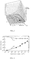
- The 3D surface plot in
fig. 7 shows an experimental verification of the algorithm efficiency as a function of nr and the mr/mref-ratio detection level. The tBD times (either SBD or HBD) of a set of NMOS transistors with 2.4 nm gate oxide thickness stressed in inversion at 4.4V were determined through visual inspection of the I(t) curves measured till HBD. Some I(t) curves showing a slow gradual increase of the noise were discarded from the original dataset, as it was too hard to unambiguously pinpoint the SBD time on them. Note that once the SBD detection algorithm according to the invention is tuned properly, it can be used to determine the SBD time for the "problem" I(t) curves as well. The selection process yielded 256 I(t) curves with either a sufficiently clear SBD signature, or none at all (HBD): 94 on L×W=1×100µm2, 64 on L×W=0.2×10µm2 and 98 on L×W=0.18×10µm2 transistors. - The tBD values determined by visual inspection were then used as a reference for validation of the tBD values found by the noise based detection algorithm for nr values from 11 to 30, mr/mref-ratio's from 1.2 to 5 in steps of 0.2 and a fixed nref = 60 value (twice the larger nr value). The percentage of false detections (tBD significantly deviating from the reference tBD value) were then plotted as a function of nr and mr/mref (
fig. 7 ) . - Clearly, lower nr and mr/mref values lead to an extremely high percentage of false early SBD detections (above 50%). In this region of the plot, the experimental α risk dominates. On the other hand, higher nr and mr/mref values lead to a relatively high percentage of late detections (above 5%): the experimental β risk dominates in that region of the plot. Thus, the surface shows a diagonal valley of reliable detection, with an overall optimum of 3/256 near nr=24 & mr/mref=2.4 (region 35). It should be noted however, that the verification was performed using a dataset acquired on relatively small gate areas.
- In the following paragraphs, the applicability range of the algorithm as a function of capacitor area and stress voltage, specific problems like the detection of early breakdowns and the sensitivity to RTS signals, and some hardware limitations are considered.
- In
fig. 8 the value of the local noise estimator mr before (curve 40) and after breakdown (curve 41) is plotted for capacitors with different areas. It is to be noted that the data forfigures 8 &9 are from capacitors stressed in accumulation. Oxide thickness was fixed at 2.4 nm, except for the smallest area where a capacitor with 2.2 nm oxide thickness was used (all values are optical thicknesses). It is clear that the detection margin closes for large area capacitors as the pre-breakdown gate current noise level increases steadily, but even for an area of 5 mm2 the noise before and after breakdown differs by 1 order of magnitude, which is sufficient for a reliable detection. It is to be noted that the post-breakdown noise is relatively independent of the area, meaning that this noise is indeed a signature of the localized soft breakdown spot. - One can speculate that the noise monitor of the invention will be unable to detect breakdown for very large capacitor areas. This is, however, irrelevant since for this thickness, measurements on capacitors larger than 5 mm2 become impossible because of the non-uniformity of the stress caused by series resistance of the polysilicon gate. Anyhow, larger optimal values for nr, mr/mref and nref than those found during the verification of the algorithm will probably be necessary to enhance the distinctive power of the algorithm for reliable SBD detection on larger areas.
Fig. 9 shows the detection margin for a 1 mm2 capacitor as a function of the stress voltage. There is no apparent dependence of both the pre- and the post-breakdown noise levels (curves 42 and 43) on stress voltage, implying that noise can be used at any stress voltage in the typical high voltage test range. - In practice it is possible that a breakdown (either soft or hard) occurs before (nref-1) Δ values have been acquired, so that no proper mref value is available yet. The algorithm can be protected against this by requiring an extra user-specified σref input. Note that mr has to be converted into the corresponding σr estimator (see Appendix 1) to test a proper σr/σref ratio as long as mref is not available.
- Fast and sufficiently long RTS signals like the one shown in
fig.10 can be misinterpreted by the algorithm as a noise increase and trigger faulty detection. Depending on the nr setting, the sorted range statistic will fill up from right to left with the larger range values and trigger detection when its middle is reached. This can be countered by larger nr and nref settings at the expense of time resolution. - Obviously, the background noise of the measurement system must be smaller than the signature noise attributed to SBD. Moreover, the resolution of the current meter must be such that it is capable of measuring the noise before breakdown. Digital current meters return quantised current levels when the true current fluctuations are close to their resolution limit, resulting in occasional zero mref values. The algorithm can be protected against this by replacing any of the corresponding zero σref values with the user-specified σref value, if occurring.
As the system has to be protected against the short currents that can occur at HBD, the voltage source compliance setting can be used as a separate trigger for HBD. Moreover, some voltage sources return a constant measured current value when in compliance. The noise detection algorithm cannot be used for detection of the HBD event then, so that this separate HBD trigger is even mandatory for such configurations. - Concluding, the present invention is related to an accurate and robust triggering algorithm for soft breakdown based on gate current noise increase that is sufficiently reliable to be applied for real-time, automatic BD detection, with acceptable execution speed if implemented properly. Triggering on current spikes or pre-BD events is avoided. This test assures correct SBD-detection in a wide range of stress conditions and various geometries. The efficiency of the algorithm and the influence of its parameters have been discussed.
- This appendix explains how the concept of a robust σ estimator originates from Statistical Process Control (SPC) and derives the relationship between the median moving range and the corresponding sigma predictor for a Normally distributed signal.
- In a production environment, a process is under control when the variation of a chosen output parameter is within a given required tolerance. The capability of a process is defined as the ratio between this tolerance and the lowest achievable output variation. Statistical process control (SPC) is the method of choice to assess this capability, and to timely detect significant deviations from the target output. In this context, the mean moving range E(r) of a process characteristic signal is often used to predict its short term variation. The historical data used for that purpose often show slow process drifts, so that the historical sample standard deviation s' becomes significantly larger than the true short term random deviation σ reflecting the process capability. The mean moving range filters out most of the signal drift, if occurring. Nevertheless, a sufficient amount of historical data is needed to reliably predict the true population σ value using a predictor based on the mean moving range. In practice, a sufficiently long process characteristic even shows sudden shifts caused by input parameter adjustments (e.g. to correct for a known drift due to machine wearout). Such shifts show up as outliers in the moving range statistic. The mean moving range is linearly sensitive to outliers, so that a σ predictor based on it can become artificially larger and cause an underestimation of the process capability. In the context of the noise-based trigger algorithm, steps and RTS-like signals can also be seen as sudden shifts of the characteristic signal. The median moving range mr even filters out such outliers, so that a σ predictor based on it will be more robust against that type of non-Normality of the signal.
- The proof is based on the properties of a Poisson process. The density function f(x) of the signal is that of the Normal distribution N(µ,σ,x) :

- Due to the independence of subsequent data points, the distribution of their differences is equivalent to the difference of two Normally distributed stochastic variables with the same spread: N(0,√2σ,x). The moving range statistic (with a subgroup size of 2) consists of taking the absolute value of those differences, thus mirroring the left side of the density function to the right. Due to the symmetry of the density function, this simply doubles the part to the right of the vertical axis. Thus, the moving range distribution has the following single-sided density function:


- This appendix shows how the execution time of the algorithm can be reduced considerably by using indirect insertion sorting for the real-time computation of both median moving range values. This approach even allows to store only a single array of (nref-1) range values in memory and to perform the indirect insertion sort for both mr and mref using 2 arrays of indices to that same Δ subset. The procedure is explained using a step by step example on the following sample I(t) dataset (arbitrary units) with nr=6 and nref=12:
t I 1 105 2 100 3 102 4 99 5 101 6 100 7 98 8 99 9 100 10 119 11 111 12 99 13 81 14 113 15 88 16 103 17 117 18 103 - Initially, the array of range values has to be filled, and the corresponding indirect insertion sort can be performed on the index arrays Lng_rng_indx & Sh_rng_indx as each new Δ value is padded to the end of the array:
Lng_rng_vec (size 11) Lng_rng_indx (size 11) Sh_rng_indx (size 5) [5] [1] [1] Insertion sort => [1] [1] [5,2] [1, 2] [1, 2] Insertion sort => [2, 1] [2, 1] [5,2,3] [2, 1, 3] [2, 1, 3] Insertion sort => [2, 3, 1] [2, 3, 1] [5, 2, 3, 2] [2, 3, 1, 4] [2, 3, 1, 4] Insertion sort => [2, 4, 3, 1] [2, 4, 3, 1] [5, 2, 3, 2, 1] [2, 4, 3, 1, 5] [2, 4, 3, 1, 5] Insertion sort => [5, 2, 4, 3, 1] [5, 2, 4, 3, 1] - At this step, the index array Sh_rng_indx is filled. Because the indices are uniquely defined, it is possible to continue as follows:
- determine the index ks,rem of the data point to be removed from the sorted range sample (bold in the table above). It can be computed from the running Lng_rng_indx pointer value kl:

- spot the index of the data point to be removed in the index array.
- pinch it from the index array.
- pad the index of the new data point at the end of the index array.
- perform an indirect insertion sort using the index array. The latter task can be performed using one time saving pass of the bisection algorithm because the other indices are already properly ordered. This is shown for the next 6 steps below.
- Notice how the
index 9 of the first large range value 19 stays at the upper end of both Lng_rng_indx & Sh_rng_indx.
At this step, the index array Lng_rng_indx is filled. The index kl,rem of the data point to be removed from that sorted range sample (bold in the table above) can be computed from the running range counter value kΔ=12:
Lng_rng_vec [18, 2, 3, 2, 1, 2, 1, 1, 19, 8, 12] Lng_rng_indx [5, 7, 8, 2, 4, 6, 3, 10, 11, 9, 1] Insertion sort ⇒ [5, 7, 8, 2, 4, 6, 3, 10, 11, 1, 9] 9, Sh_rng_indx [8, 10, 11, 1] 1] Insertion sort ⇒ [8, 10, 11, 1, 9] Lng_rng_vec [18, 32, 3, 2, 1, 2, 1, 1, 19, 8, 12] Lng_rng_indx [5, 7, 8, 4, 6, 3, 10, 11, 1, 9, 2] Insertion sort ⇒ [5, 7, 8, 4, 6, 3, 10, 11, 1, 9, 2] Sh_rng_indx [10, 11, 1, 9, 2] Insertion sort ⇒ [10, 11, 1, 9, 2] - At this step, the median moving range ratio could lead to detection, and subsequent exit of the algorithm:

| Lng_rng_vec | [5, 2, 3, 2, 1, 2] |
| Lng_rng_indx | [5, 2, 4, 3, 1, 6] |
| Insertion sort ⇒ | [5, 2, 4, 6, 3, 1] |
| Sh_rng_indx | [5, 2, 4, 3, 6] |
| Insertion sort ⇒ | [5, 2, 4, 6, 3] |
| Lng_rng_vec | [5, 2, 3, 2, 1, 2, 1] |
| Lng_rng_indx | [5, 2, 4, 6, 3, 1, 7] |
| Insertion sort => | [5, 7, 2, 4, 6, 3, 1] 3, |
| Sh_rng_indx | [5, 4, 6, 7] |
| Insertion sort => | [5, 7, 4, 6, 3] |
| Lng_rng_vec | [5, 2, 3, 2, 1, 2, 1, 1] |
| Lng_rng_indx | [5, 7, 2, 4, 6, 3, 1, 8] |
| Insertion sort ⇒ | [5, 7, 8, 2, 4, 6, 3, 1] |
| Sh_rng_indx | [5, 7, 4, 6, 8] |
| Insertion sort ⇒ | [5, 7, 8, 4, 6] |
| Lng_rng_vec | [5, 2, 3, 2, 1, 2, 1, 1, 19] |
| Lng_rng_indx | [5, 7, 8, 2, 4, 6, 3, 1, 9] |
| Insertion sort => | [5, 7, 8, 2, 4, 6, 3, 1, 9] |
| Sh_rng_indx | [5, 7, 8, 6, 9] |
| Insertion sort ⇒ | [5, 7, 8, 6, 9] |
| Lng_rng_vec | [5, 2, 3, 2, 1, 2, 1, 1, 19, 8] |
| Lng_rng_indx | [5, 7, 8, 2, 4, 6, 3, 1, 9, 10] |
| Insertion sort => | [5, 7, 8, 2, 4, 6, 3, 1, 10, 9] |
| Sh_rng_indx | |
| Insertion sort => | [7, 8, 6, 9, 10] [7, 8, 6, 10, 9] |
| Lng_rng_vec | [5, 2, 3, 2, 1, 2, 1, 1, 19, 8, 12] |
| Lng_rng_indx | [5, 7, 8, 2, 4, 6, 3, 1, 10, 9, 11] |
| Insertion sort ⇒ | [5, 7, 8, 2, 4, 6, 3, 1, 10, 11, 9] |
| Sh_rng_ | [7, 8, 10, 9, 11] |
| Insertion sort | [7, 8, 10, 11, 9] |
Claims (5)
- A method for detecting breakdown (1, 12) in a dielectric layer, comprising the steps of:- applying a signal to said dielectric layer,- measuring a plurality of sets of readings having values, which are in relation to said signal,- searching and identifying outlier readings in each of said sets, said outlier readings being defined by the fact that they have values which are significantly higher or lower than the majority of the values of said set,- selecting from each of said sets, one reading which is not one of said outlier readings,- comparing the value of said one selected reading to a reference value, so that the exceeding of said value leads to the conclusion that a predefined probability is present for having a breakdown state in said layer,characterized in that- for each set of readings, a second set of readings is measured, said second set consisting of at least twice the amount of readings of said first set of readings, and wherein said reference value is a function of the value of a selected reading of said second set, said selected reading being selected in the same way as said selected reading of said first set, and- the value of said selected reading of said second set is the median (mref) of the values of said second set of readings, and- said function is a linear function f (mref) = amref, with a predefined factor 'a'.
- The method according to claim 1, wherein the value of said one selected reading is the median (mr) of the values of said first set of readings.
- A method according to any one of claims 1 to 2, wherein the sorting of said sets of readings is done according to an indirect insertion sorting technique.
- A method according to claim 3, wherein said signal is a voltage signal, corresponding to a voltage difference across said layer, and said readings are absolute values of the change of the current flowing through said layer, as a consequence of said voltage signal, said change being calculated on the basis of a set of current readings, as the difference between two subsequent current readings of said set.
- A method according to claim 3, wherein said signal is a current signal, corresponding to a current flowing through said layer, and said readings are absolute values of the change of the voltage across said layer, as a consequence of said current signal, said change being calculated on the basis of a set of voltage readings, as the difference between two subsequent voltage readings of said set.
Applications Claiming Priority (2)
| Application Number | Priority Date | Filing Date | Title |
|---|---|---|---|
| US28702801P | 2001-04-27 | 2001-04-27 | |
| US287028P | 2001-04-27 |
Publications (3)
| Publication Number | Publication Date |
|---|---|
| EP1276144A2 EP1276144A2 (en) | 2003-01-15 |
| EP1276144A3 EP1276144A3 (en) | 2009-06-24 |
| EP1276144B1 true EP1276144B1 (en) | 2019-02-27 |
Family
ID=23101166
Family Applications (1)
| Application Number | Title | Priority Date | Filing Date |
|---|---|---|---|
| EP02447071.8A Expired - Lifetime EP1276144B1 (en) | 2001-04-27 | 2002-04-22 | A method and apparatus for detecting breakdown in ultra thin dielectric layers. |
Country Status (2)
| Country | Link |
|---|---|
| US (1) | US6777972B2 (en) |
| EP (1) | EP1276144B1 (en) |
Families Citing this family (3)
| Publication number | Priority date | Publication date | Assignee | Title |
|---|---|---|---|---|
| JP4051332B2 (en) * | 2003-11-07 | 2008-02-20 | 株式会社日立ハイテクノロジーズ | Inspection data analysis system |
| US8493075B2 (en) | 2010-09-08 | 2013-07-23 | International Business Machines Corporation | Method and apparatus for preventing circuit failure |
| US9285417B2 (en) | 2013-01-02 | 2016-03-15 | Globalfoundries Inc. | Low-voltage IC test for defect screening |
Family Cites Families (3)
| Publication number | Priority date | Publication date | Assignee | Title |
|---|---|---|---|---|
| US5804975A (en) * | 1996-09-18 | 1998-09-08 | Lucent Technologies Inc. | Detecting breakdown in dielectric layers |
| US6255841B1 (en) * | 1999-05-20 | 2001-07-03 | Lucent Technologies, Inc. | Statistical system and method for testing integrated circuits |
| JP2001021609A (en) * | 1999-07-07 | 2001-01-26 | Mitsubishi Electric Corp | Inspection method for semiconductor integrated circuit |
-
2002
- 2002-04-22 EP EP02447071.8A patent/EP1276144B1/en not_active Expired - Lifetime
- 2002-04-22 US US10/127,381 patent/US6777972B2/en not_active Expired - Lifetime
Non-Patent Citations (1)
| Title |
|---|
| None * |
Also Published As
| Publication number | Publication date |
|---|---|
| US20030016046A1 (en) | 2003-01-23 |
| US6777972B2 (en) | 2004-08-17 |
| EP1276144A3 (en) | 2009-06-24 |
| EP1276144A2 (en) | 2003-01-15 |
Similar Documents
| Publication | Publication Date | Title |
|---|---|---|
| US8266572B2 (en) | Method for acquiring overshoot voltage and analyzing degradation of a gate insulation using the same | |
| US20110031981A1 (en) | Valuation method of dielectric breakdown lifetime of gate insulating film, valuation device of dielectric breakdown lifetime of gate insulating film and program for evaluating dielectric breakdown lifetime of gate insulating film | |
| US6242934B1 (en) | Background leakage zeroing by temperature and voltage dependence for IDDQ measurement and defect resolution | |
| US6326792B1 (en) | Method and apparatus for lifetime prediction of dielectric breakdown | |
| US5485097A (en) | Method of electrically measuring a thin oxide thickness by tunnel voltage | |
| US5804975A (en) | Detecting breakdown in dielectric layers | |
| US5793212A (en) | Method of measuring the breakdown charge of a dielectric film | |
| KR101074832B1 (en) | System and method for classifying defects in electrical circuits and recognizing process problems for electrical circuits | |
| US6014034A (en) | Method for testing semiconductor thin gate oxide | |
| EP1276144B1 (en) | A method and apparatus for detecting breakdown in ultra thin dielectric layers. | |
| Roussel et al. | Accurate and robust noise-based trigger algorithm for soft breakdown detection in ultrathin gate dielectrics | |
| Alers et al. | J-ramp on sub-3 nm dielectrics: noise as a breakdown criterion | |
| US6524872B1 (en) | Using fast hot-carrier aging method for measuring plasma charging damage | |
| US6528335B2 (en) | Electrical method for assessing yield-limiting asperities in silicon-on-insulator wafers | |
| KR100640637B1 (en) | Defect Detection of Time-Dependent Dielectric Breakdown Characteristics of Morse Transistors Designed in Circuits | |
| Van Beek et al. | Ultrafast RVS as an efficient method to measure oxide breakdown in the EOS and ESD time domain | |
| Balachandran et al. | Improvement of SRAM-based failure analysis using calibrated Iddq testing | |
| US12158442B2 (en) | IC structure moisture ingress detection by current hump in current-voltage response curve | |
| JP2007258488A (en) | Insulation film dielectric breakdown lifetime estimation method | |
| JP2584093B2 (en) | Insulation film reliability evaluation method | |
| US7315974B2 (en) | Method for detecting faults in electronic devices, based on quiescent current measurements | |
| US6858448B2 (en) | Method for evaluating and manufacturing a semiconductor device | |
| KR100515880B1 (en) | Method for measuring breakdown voltage of gate oxide | |
| JP3631472B2 (en) | Semiconductor device evaluation method, semiconductor device manufacturing method, and semiconductor device evaluation apparatus and evaluation program | |
| JP2013065901A (en) | Automatic dynamic baseline creation and adjustment |
Legal Events
| Date | Code | Title | Description |
|---|---|---|---|
| PUAI | Public reference made under article 153(3) epc to a published international application that has entered the european phase |
Free format text: ORIGINAL CODE: 0009012 |
|
| AK | Designated contracting states |
Kind code of ref document: A2 Designated state(s): AT BE CH CY DE DK ES FI FR GB GR IE IT LI LU MC NL PT SE TR |
|
| AX | Request for extension of the european patent |
Free format text: AL;LT;LV;MK;RO;SI |
|
| PUAL | Search report despatched |
Free format text: ORIGINAL CODE: 0009013 |
|
| AK | Designated contracting states |
Kind code of ref document: A3 Designated state(s): AT BE CH CY DE DK ES FI FR GB GR IE IT LI LU MC NL PT SE TR |
|
| AX | Request for extension of the european patent |
Extension state: AL LT LV MK RO SI |
|
| RAP1 | Party data changed (applicant data changed or rights of an application transferred) |
Owner name: IMEC |
|
| 17P | Request for examination filed |
Effective date: 20091127 |
|
| AKX | Designation fees paid |
Designated state(s): AT BE CH CY DE DK ES FI FR GB GR IE IT LI LU MC NL PT SE TR |
|
| 17Q | First examination report despatched |
Effective date: 20100308 |
|
| STAA | Information on the status of an ep patent application or granted ep patent |
Free format text: STATUS: EXAMINATION IS IN PROGRESS |
|
| RAP1 | Party data changed (applicant data changed or rights of an application transferred) |
Owner name: IMEC VZW |
|
| GRAP | Despatch of communication of intention to grant a patent |
Free format text: ORIGINAL CODE: EPIDOSNIGR1 |
|
| STAA | Information on the status of an ep patent application or granted ep patent |
Free format text: STATUS: GRANT OF PATENT IS INTENDED |
|
| INTG | Intention to grant announced |
Effective date: 20180913 |
|
| GRAS | Grant fee paid |
Free format text: ORIGINAL CODE: EPIDOSNIGR3 |
|
| GRAA | (expected) grant |
Free format text: ORIGINAL CODE: 0009210 |
|
| STAA | Information on the status of an ep patent application or granted ep patent |
Free format text: STATUS: THE PATENT HAS BEEN GRANTED |
|
| RIC1 | Information provided on ipc code assigned before grant |
Ipc: H01L 21/66 20060101AFI20021120BHEP |
|
| AK | Designated contracting states |
Kind code of ref document: B1 Designated state(s): AT BE CH CY DE DK ES FI FR GB GR IE IT LI LU MC NL PT SE TR |
|
| REG | Reference to a national code |
Ref country code: GB Ref legal event code: FG4D |
|
| REG | Reference to a national code |
Ref country code: CH Ref legal event code: EP |
|
| REG | Reference to a national code |
Ref country code: DE Ref legal event code: R096 Ref document number: 60249798 Country of ref document: DE |
|
| REG | Reference to a national code |
Ref country code: AT Ref legal event code: REF Ref document number: 1102555 Country of ref document: AT Kind code of ref document: T Effective date: 20190315 |
|
| REG | Reference to a national code |
Ref country code: IE Ref legal event code: FG4D |
|
| REG | Reference to a national code |
Ref country code: NL Ref legal event code: MP Effective date: 20190227 |
|
| PG25 | Lapsed in a contracting state [announced via postgrant information from national office to epo] |
Ref country code: NL Free format text: LAPSE BECAUSE OF FAILURE TO SUBMIT A TRANSLATION OF THE DESCRIPTION OR TO PAY THE FEE WITHIN THE PRESCRIBED TIME-LIMIT Effective date: 20190227 Ref country code: SE Free format text: LAPSE BECAUSE OF FAILURE TO SUBMIT A TRANSLATION OF THE DESCRIPTION OR TO PAY THE FEE WITHIN THE PRESCRIBED TIME-LIMIT Effective date: 20190227 Ref country code: PT Free format text: LAPSE BECAUSE OF FAILURE TO SUBMIT A TRANSLATION OF THE DESCRIPTION OR TO PAY THE FEE WITHIN THE PRESCRIBED TIME-LIMIT Effective date: 20190627 Ref country code: FI Free format text: LAPSE BECAUSE OF FAILURE TO SUBMIT A TRANSLATION OF THE DESCRIPTION OR TO PAY THE FEE WITHIN THE PRESCRIBED TIME-LIMIT Effective date: 20190227 |
|
| PG25 | Lapsed in a contracting state [announced via postgrant information from national office to epo] |
Ref country code: GR Free format text: LAPSE BECAUSE OF FAILURE TO SUBMIT A TRANSLATION OF THE DESCRIPTION OR TO PAY THE FEE WITHIN THE PRESCRIBED TIME-LIMIT Effective date: 20190528 |
|
| REG | Reference to a national code |
Ref country code: AT Ref legal event code: MK05 Ref document number: 1102555 Country of ref document: AT Kind code of ref document: T Effective date: 20190227 |
|
| PG25 | Lapsed in a contracting state [announced via postgrant information from national office to epo] |
Ref country code: DK Free format text: LAPSE BECAUSE OF FAILURE TO SUBMIT A TRANSLATION OF THE DESCRIPTION OR TO PAY THE FEE WITHIN THE PRESCRIBED TIME-LIMIT Effective date: 20190227 Ref country code: ES Free format text: LAPSE BECAUSE OF FAILURE TO SUBMIT A TRANSLATION OF THE DESCRIPTION OR TO PAY THE FEE WITHIN THE PRESCRIBED TIME-LIMIT Effective date: 20190227 Ref country code: IT Free format text: LAPSE BECAUSE OF FAILURE TO SUBMIT A TRANSLATION OF THE DESCRIPTION OR TO PAY THE FEE WITHIN THE PRESCRIBED TIME-LIMIT Effective date: 20190227 |
|
| REG | Reference to a national code |
Ref country code: DE Ref legal event code: R097 Ref document number: 60249798 Country of ref document: DE |
|
| REG | Reference to a national code |
Ref country code: CH Ref legal event code: PL |
|
| REG | Reference to a national code |
Ref country code: BE Ref legal event code: MM Effective date: 20190430 |
|
| PG25 | Lapsed in a contracting state [announced via postgrant information from national office to epo] |
Ref country code: AT Free format text: LAPSE BECAUSE OF FAILURE TO SUBMIT A TRANSLATION OF THE DESCRIPTION OR TO PAY THE FEE WITHIN THE PRESCRIBED TIME-LIMIT Effective date: 20190227 Ref country code: MC Free format text: LAPSE BECAUSE OF FAILURE TO SUBMIT A TRANSLATION OF THE DESCRIPTION OR TO PAY THE FEE WITHIN THE PRESCRIBED TIME-LIMIT Effective date: 20190227 Ref country code: LU Free format text: LAPSE BECAUSE OF NON-PAYMENT OF DUE FEES Effective date: 20190422 |
|
| PLBE | No opposition filed within time limit |
Free format text: ORIGINAL CODE: 0009261 |
|
| STAA | Information on the status of an ep patent application or granted ep patent |
Free format text: STATUS: NO OPPOSITION FILED WITHIN TIME LIMIT |
|
| GBPC | Gb: european patent ceased through non-payment of renewal fee |
Effective date: 20190527 |
|
| PG25 | Lapsed in a contracting state [announced via postgrant information from national office to epo] |
Ref country code: LI Free format text: LAPSE BECAUSE OF NON-PAYMENT OF DUE FEES Effective date: 20190430 Ref country code: CH Free format text: LAPSE BECAUSE OF NON-PAYMENT OF DUE FEES Effective date: 20190430 |
|
| 26N | No opposition filed |
Effective date: 20191128 |
|
| PG25 | Lapsed in a contracting state [announced via postgrant information from national office to epo] |
Ref country code: BE Free format text: LAPSE BECAUSE OF NON-PAYMENT OF DUE FEES Effective date: 20190430 |
|
| PG25 | Lapsed in a contracting state [announced via postgrant information from national office to epo] |
Ref country code: TR Free format text: LAPSE BECAUSE OF FAILURE TO SUBMIT A TRANSLATION OF THE DESCRIPTION OR TO PAY THE FEE WITHIN THE PRESCRIBED TIME-LIMIT Effective date: 20190227 |
|
| PG25 | Lapsed in a contracting state [announced via postgrant information from national office to epo] |
Ref country code: IE Free format text: LAPSE BECAUSE OF NON-PAYMENT OF DUE FEES Effective date: 20190422 Ref country code: GB Free format text: LAPSE BECAUSE OF NON-PAYMENT OF DUE FEES Effective date: 20190527 |
|
| PGFP | Annual fee paid to national office [announced via postgrant information from national office to epo] |
Ref country code: FR Payment date: 20200319 Year of fee payment: 19 |
|
| PGFP | Annual fee paid to national office [announced via postgrant information from national office to epo] |
Ref country code: DE Payment date: 20200319 Year of fee payment: 19 |
|
| PG25 | Lapsed in a contracting state [announced via postgrant information from national office to epo] |
Ref country code: CY Free format text: LAPSE BECAUSE OF FAILURE TO SUBMIT A TRANSLATION OF THE DESCRIPTION OR TO PAY THE FEE WITHIN THE PRESCRIBED TIME-LIMIT Effective date: 20190227 |
|
| REG | Reference to a national code |
Ref country code: DE Ref legal event code: R119 Ref document number: 60249798 Country of ref document: DE |
|
| PG25 | Lapsed in a contracting state [announced via postgrant information from national office to epo] |
Ref country code: DE Free format text: LAPSE BECAUSE OF NON-PAYMENT OF DUE FEES Effective date: 20211103 Ref country code: FR Free format text: LAPSE BECAUSE OF NON-PAYMENT OF DUE FEES Effective date: 20210430 |