EP1276144A2 - A method and apparatus for detecting breakdown in ultra thin dielectric layers. - Google Patents
A method and apparatus for detecting breakdown in ultra thin dielectric layers. Download PDFInfo
- Publication number
- EP1276144A2 EP1276144A2 EP02447071A EP02447071A EP1276144A2 EP 1276144 A2 EP1276144 A2 EP 1276144A2 EP 02447071 A EP02447071 A EP 02447071A EP 02447071 A EP02447071 A EP 02447071A EP 1276144 A2 EP1276144 A2 EP 1276144A2
- Authority
- EP
- European Patent Office
- Prior art keywords
- readings
- values
- current
- breakdown
- signal
- Prior art date
- Legal status (The legal status is an assumption and is not a legal conclusion. Google has not performed a legal analysis and makes no representation as to the accuracy of the status listed.)
- Granted
Links
Images

Classifications
-
- H—ELECTRICITY
- H10—SEMICONDUCTOR DEVICES; ELECTRIC SOLID-STATE DEVICES NOT OTHERWISE PROVIDED FOR
- H10P—GENERIC PROCESSES OR APPARATUS FOR THE MANUFACTURE OR TREATMENT OF DEVICES COVERED BY CLASS H10
- H10P74/00—Testing or measuring during manufacture or treatment of wafers, substrates or devices
- H10P74/20—Testing or measuring during manufacture or treatment of wafers, substrates or devices characterised by the properties tested or measured, e.g. structural or electrical properties
- H10P74/203—Structural properties, e.g. testing or measuring thicknesses, line widths, warpage, bond strengths or physical defects
Definitions
- Oxide breakdown is one of the most threatening failure mechanisms in integrated circuits. As the oxide thickness is decreased in the sub-5nm range, the breakdown definition itself is no longer clear and its detection becomes problematic.
- the present invention is related to methods of detecting the breakdown in dielectric layers, in particular oxide layers of such low thickness.
- SBD is usually associated with a smaller current jump during a Constant Voltage Stress (CVS) or a smaller voltage drop during Constant Current Stress (CCS) compared to the HBD case.
- CVS Constant Voltage Stress
- CCS Constant Current Stress
- the soft and hard breakdowns are caused by the same physical mechanism: SBD is considered to be a breakdown without the thermal runaway effects that lead to a low-resistance breakdown path connecting gate and substrate [1].
- SBD occurs when the generated density of traps during a CVS or CCS has sufficiently increased to generate (at some random place on the capacitor area) a breakdown path of traps connecting anode with cathode.
- SBD is (just as HBD) a local event.
- Ig-Vg characteristic of the SBD is, apart from some statistical fluctuations, independent of the test area [3].
- This IV-curve is the most unambiguous signature of an SBD event, and measuring it is therefore the most direct way to detect SBD.
- this approach has the disadvantage that the stress needs to be interrupted at regular time intervals to measure the low voltage current. This is time-consuming and might influence the time-to-breakdown, especially when the current or voltage overshoot at the start of each stress interval is not well-controlled.
- the present invention aims to provide a accurate method for detecting soft breakdown events in integrated circuit devices, wherein a reduced sensitivity is present to pre-breakdown events, resulting in a lower probability of erroneous breakdown detection.
- the present invention is related to a method for detecting breakdown in a dielectric layer, comprising the steps of:
- the value of said one selected reading is the median (m r ) of the values of said set of readings.
- a second set of readings is measured, said second set consisting of at least twice the amount of readings of said first set of readings, and wherein said reference value is a function of the value of a selected reading of said second set, said selected reading being selected in the same way as said selected reading of said first set.
- the value of said selected reading of said second set is the median (m ref ) of the values of said second set of readings.
- the sorting of said sets of readings is preferably done according to an indirect insertion sorting technique.
- said signal is a voltage signal, corresponding to a voltage difference across said layer, and said readings are absolute values of the change of the current flowing through said layer, as a consequence of said voltage signal, said change being calculated on the basis of a set of current readings, as the difference between two subsequent current readings of said set.
- said signal is a current signal, corresponding to a current flowing through said layer, and said readings are absolute values of the change of the voltage across said layer, as a consequence of said current signal, said change being calculated on the basis of a set of voltage readings, as the difference between two subsequent voltage readings of said set.
- the invention is equally related to an apparatus for detecting breakdown in a dielectric layer, said apparatus comprising:
- said means for calculating comprises means for sorting said sets of readings according to an indirect insertion sorting technique.
- said test signal may be a voltage signal, corresponding to a voltage difference across said layer, in which case said readings are absolute values of current changes.
- said test signal may be a current signal, corresponding to a current through said layer, in which case said readings are absolute values of voltage changes.
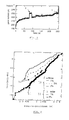
- Figure 1 illustrates the gate current of an NMOS transistor as a function of time, until breakdown occurs.
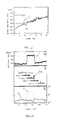
- Figure 2 represents the Weibull distributions of time-to-breakdown for a small and large device, for different trigger methodologies.
- Figure 3 illustrates the relation between the detection level and the current increase upon breakdown.
- Figure 4 illustrates the capability of different noise estimators to avoid false breakdown detection.
- Figure 5 illustrates the capability of the method of the invention to detect an actual breakdown event.
- Figure 6 illustrates the detection of breakdown with the help of a running reference value for the noise estimator.
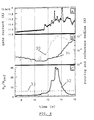
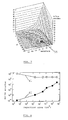
- FIG. 7 gives an overview of the influence of several parameters on the accuracy of the detection algorithm.
- Figure 8 is showing the relation between the detection capabilities of the method of invention, and the capacitor area involved.
- Figure 9 is showing the same relation as figure 8, but for small devices only.
- Figure 10 illustrates problems that may arise in the case of long RTS-like signals.
- the present invention is related to a new optimized trigger algorithm for SBD based on gate current noise increase that is sufficiently reliable to be applied for real-time, automatic BD detection. Automated BD tests often stress the devices till HBD occurs. The method according to the invention even allows interruption of the CVS upon detection of SBD, resulting in considerably shorter overall test times.
- the current vs. time behaviour in small dimension transistors during a Constant Voltage Stress shows RTS-like events 2 as illustrated in fig. 1.
- These gate current jumps are not breakdowns, but pre-breakdown events because the t BD -distributions obtained on two different areas by triggering on these jumps do not line up after the well-known area scaling law has been applied.
- a 5 percent step trigger is needed to approximate the noise-triggered distribution. Only the noise-triggered distributions line up for both areas, proving that the gate current steps observed in small area devices are not breakdowns, but pre-breakdown events.
- the simplest approach to applying noise for breakdown detection is monitoring the sample standard deviation of a number of gate current values, preferably in a subset containing a fixed number n r of consecutive current measurements including the last measured value.
- the set should be chosen sufficiently large to generate statistically relevant parameters, but it should still be sufficiently small to allow for an acceptable time resolution.
- the 'running' estimate s' for the standard deviation ⁇ will increase when the gate current noise increases at breakdown.
- the present invention solves this problem in an elegant way by selecting a value of the ⁇ set which is not an outlier value, as the breakdown monitor.
- An outlier value can then be defined as a value which is significantly higher or lower than the majority of values in the set.
- outlier values are identified by the fact that they exceed a predefined border value, such 10 -9 A in the example above.
- the selected value is the median m r of the ⁇ set.
- finding the median of a dataset consists of sorting the data and taking the middle value as the central value estimator, see the vertical arrows above each set of ⁇ I-values.
- the average of the middle two values is taken. This complication can be avoided by requiring an odd number of ⁇ values.
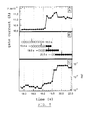
- curve 23 shows the evolution of m r as a function of time. m r is not increased by the gate current peak, which introduces only one high ⁇ I-value in the set, which in turn does not affect the running median m r .
- a running reference value is constructed along with the running non-outlier value, preferably the median m r .
- the running reference is constructed in an identical way as m r , but it is based on n ref current values, with n ref >2•n r .
- a second set of n ref -1 current changes is calculated on the basis of the n ref current values, and the running reference is selected as a non-outlier value of said second set.
- the running reference is the median m ref of said second set. Breakdown is triggered when a significant difference between m ref and m r is detected, or equivalently, when the ratio m r /m ref exceeds a given value 'a'.
- the median m r is compared to a reference value which is preferably a linear function a.m ref , of the reference median m ref .
- a.m ref a linear function of the reference median m ref .
- breakdown is detected with a predefined probability.
- this can be done with a one-sided F-ratio test on ⁇ r 2 / ⁇ ref 2 or equivalently, m r 2 /m ref 2 with (n r -1, n ref -1) degrees of freedom.
- this test simply reduces to finding when the square root of the F-ratio exceeds a fixed detection threshold which can be calculated before the stress measurement starts.
- a default 99.73% value for the significance probability is preferably chosen, as this corresponds with the 3 ⁇ limits for a normally distributed signal, which is commonly used for statistical process control purposes.
- Fig. 6A shows the current increase due to SBD.
- Curves 30 and 31 represent the m r and m ref values, as a function of time.
- the m r -curve 30 shows a rather gradual increase, making it difficult for a simple step detecting algorithm to trigger properly.
- Fig. 6C shows the evolution of the ratio m r /m ref .
- the real-time detection algorithm has to be designed in a computationally efficient way, so that it can keep up with the stream of incoming current values from the measurement hardware. Performing a complete sort of each range subset upon acquisition of a new current value would take a considerable amount of the computation time needed by the algorithm. It is more efficient to perform an indirect insertion sort (see also reference [6]) "on the fly" on an array of moving range values stored in a cyclic way. Indirect sorting reorders an array of indices to the data points instead of the data points themselves.
- the m r /m ref ratio detection level determines the detection efficiency of the algorithm: for Gaussian noise, a higher m r /m ref ratio lowers the ⁇ risk (representing the probability of false early detections) at the expense of a higher ⁇ risk (representing the probability of overlooking a true noise increase due to SBD). A proper balance between these two risks should be determined for a given measurement setup by means of a calibration procedure.
- n r and n ref values enhance the distinctive power of the detection algorithm: both the ⁇ risk and the ⁇ risk are predictably lower for Gaussian noise.
- increasing n r and n ref also enhances the robustness of the algorithm against "non-Normal" events like spikes, pre-BD steps, and more specifically, longer RTS-like signals, as a larger amount of outlier ranges have to accumulate in the sorted moving range statistic before they reach its middle.
- using larger n r and n ref values for detection is at the expense of a lower time resolution for the t BD values: as half of the short range sample collection time is taken as the average delay time for detection, longer samples correspond with a larger uncertainty on t BD .
- the 3D surface plot in fig. 7 shows an experimental verification of the algorithm efficiency as a function of n r and the m r /m ref -ratio detection level.
- the t BD times (either SBD or HBD) of a set of NMOS transistors with 2.4 nm gate oxide thickness stressed in inversion at 4.4V were determined through visual inspection of the I(t) curves measured till HBD. Some I(t) curves showing a slow gradual increase of the noise were discarded from the original dataset, as it was too hard to unambiguously pinpoint the SBD time on them. Note that once the SBD detection algorithm according to the invention is tuned properly, it can be used to determine the SBD time for the "problem" I(t) curves as well.
- the percentage of false detections were then plotted as a function of n r and m r /m ref (fig. 7).
- n r and m r /m ref values lead to an extremely high percentage of false early SBD detections (above 50%). In this region of the plot, the experimental ⁇ risk dominates.
- higher n r and m r /m ref values lead to a relatively high percentage of late detections (above 5%): the experimental ⁇ risk dominates in that region of the plot.
- Fig. 9 shows the detection margin for a 1 mm 2 capacitor as a function of the stress voltage.
- the background noise of the measurement system must be smaller than the signature noise attributed to SBD.
- the resolution of the current meter must be such that it is capable of measuring the noise before breakdown.
- Digital current meters return quantised current levels when the true current fluctuations are close to their resolution limit, resulting in occasional zero m ref values.
- the algorithm can be protected against this by replacing any of the corresponding zero ⁇ ref values with the user-specified ⁇ ref value, if occurring.
- the voltage source compliance setting can be used as a separate trigger for HBD.
- some voltage sources return a constant measured current value when in compliance. The noise detection algorithm cannot be used for detection of the HBD event then, so that this separate HBD trigger is even mandatory for such configurations.
- the present invention is related to an accurate and robust triggering algorithm for soft breakdown based on gate current noise increase that is sufficiently reliable to be applied for real-time, automatic BD detection, with acceptable execution speed if implemented properly. Triggering on current spikes or pre-BD events is avoided. This test assures correct SBD-detection in a wide range of stress conditions and various geometries. The efficiency of the algorithm and the influence of its parameters have been discussed.
Landscapes
- Testing Or Measuring Of Semiconductors Or The Like (AREA)
- Testing Of Individual Semiconductor Devices (AREA)
- Testing Relating To Insulation (AREA)
Abstract
- applying a signal to said dielectric layer,
- measuring a plurality of sets of readings having values, which are in relation to said signal,
- searching and identifying outlier readings in each of said sets, said outlier readings being defined by the fact that they have values which are significantly higher or lower than the majority of the values of said set,
- selecting from each of said sets, one reading which is not one of said outlier readings,
- comparing the value of said one selected reading to a reference value, so that the exceeding of said value leads to the conclusion that a predefined probability is present for having a breakdown state in said layer.
Description
Depas, T. Nigam et al. IEEE Trans. Elec. Dev., vol. 43, no. 9, pp. 1499-1504, 1996.
All references between square brackets are referring to one or more of these six documents.
- applying a signal to said dielectric layer,
- measuring a plurality of sets of readings having values, which are in relation to said signal,
- searching and identifying outlier readings in each of said sets, said outlier readings being defined by the fact that they have values which are significantly higher or lower than the majority of the values of said set,
- selecting from each of said sets, one reading which is not one of said outlier readings,
- comparing the value of said one selected reading to a reference value, so that the exceeding of said value leads to the conclusion that a predefined probability is present for having a breakdown state in said layer.
- means for applying a test signal to a dielectric layer,
- means for measuring a number of sets of readings,
- means for searching and selecting one reading in each set,
- means for comparing the value of said one selected reading to a reference value,
- output means for indicating that a breakdown state is present in said layer, with a given probability, on the basis of said comparison.
In small area devices, a 5 percent step trigger is needed to approximate the noise-triggered distribution. Only the noise-triggered distributions line up for both areas, proving that the gate current steps observed in small area devices are not breakdowns, but pre-breakdown events.
As the system has to be protected against the short currents that can occur at HBD, the voltage source compliance setting can be used as a separate trigger for HBD. Moreover, some voltage sources return a constant measured current value when in compliance. The noise detection algorithm cannot be used for detection of the HBD event then, so that this separate HBD trigger is even mandatory for such configurations.


Claims (12)
- A method for detecting breakdown in a dielectric layer, comprising the steps of:applying a signal to said dielectric layer,measuring a plurality of sets of readings having values, which are in relation to said signal,searching and identifying outlier readings in each of said sets, said outlier readings being defined by the fact that they have values which are significantly higher or lower than the majority of the values of said set,selecting from each of said sets, one reading which is not one of said outlier readings,comparing the value of said one selected reading to a reference value, so that the exceeding of said value leads to the conclusion that a predefined probability is present for having a breakdown state in said layer.
- The method according to claim 1, wherein the value of said one selected reading is the median (mr) of the values of said set of readings.
- The method according to claim 1, wherein for each set of readings, a second set of readings is measured, said second set consisting of at least twice the amount of readings of said first set of readings, and wherein said reference value is a function of the value of a selected reading of said second set, said selected reading being selected in the same way as said selected reading of said first set.
- The method according to claim 3, wherein the value of said selected reading of said second set is the median (mref) of the values of said second set of readings.
- A method according to claim 4, wherein said function is a linear function f(mref) = amref, with a predefined factor 'a'.
- A method according to any one of claims 1 to 5, wherein the sorting of said sets of readings is done according to an indirect insertion sorting technique.
- A method according to claim 6, wherein said signal is a voltage signal, corresponding to a voltage difference across said layer, and said readings are absolute values of the change of the current flowing through said layer, as a consequence of said voltage signal, said change being calculated on the basis of a set of current readings, as the difference between two subsequent current readings of said set.
- A method according to claim 6, wherein said signal is a current signal, corresponding to a current flowing through said layer, and said readings are absolute values of the change of the voltage across said layer, as a consequence of said current signal, said change being calculated on the basis of a set of voltage readings, as the difference between two subsequent voltage readings of said set.
- An apparatus for detecting breakdown in a dielectric layer, said apparatus comprising:means for applying a test signal to a dielectric layer,means for measuring a number of sets of readings,means for searching and selecting one reading in each set,means for comparing the value of said one selected reading to a reference value,output means for indicating that a breakdown state is present in said layer, with a given probability, on the basis of said comparison.
- An apparatus according to claim 9, wherein said means for calculating comprises means for sorting said sets of readings according to an indirect insertion sorting technique.
- An apparatus according to claim 10, wherein said test signal is a voltage signal, corresponding to a voltage difference across said layer, and said readings are absolute values of current changes.
- An apparatus according to claim 10, wherein said test signal is a current signal, corresponding to a current through said layer, and said readings are absolute values of voltage changes.
Applications Claiming Priority (2)
| Application Number | Priority Date | Filing Date | Title |
|---|---|---|---|
| US28702801P | 2001-04-27 | 2001-04-27 | |
| US287028P | 2001-04-27 |
Publications (3)
| Publication Number | Publication Date |
|---|---|
| EP1276144A2 true EP1276144A2 (en) | 2003-01-15 |
| EP1276144A3 EP1276144A3 (en) | 2009-06-24 |
| EP1276144B1 EP1276144B1 (en) | 2019-02-27 |
Family
ID=23101166
Family Applications (1)
| Application Number | Title | Priority Date | Filing Date |
|---|---|---|---|
| EP02447071.8A Expired - Lifetime EP1276144B1 (en) | 2001-04-27 | 2002-04-22 | A method and apparatus for detecting breakdown in ultra thin dielectric layers. |
Country Status (2)
| Country | Link |
|---|---|
| US (1) | US6777972B2 (en) |
| EP (1) | EP1276144B1 (en) |
Families Citing this family (3)
| Publication number | Priority date | Publication date | Assignee | Title |
|---|---|---|---|---|
| JP4051332B2 (en) * | 2003-11-07 | 2008-02-20 | 株式会社日立ハイテクノロジーズ | Inspection data analysis system |
| US8493075B2 (en) | 2010-09-08 | 2013-07-23 | International Business Machines Corporation | Method and apparatus for preventing circuit failure |
| US9285417B2 (en) | 2013-01-02 | 2016-03-15 | Globalfoundries Inc. | Low-voltage IC test for defect screening |
Family Cites Families (3)
| Publication number | Priority date | Publication date | Assignee | Title |
|---|---|---|---|---|
| US5804975A (en) * | 1996-09-18 | 1998-09-08 | Lucent Technologies Inc. | Detecting breakdown in dielectric layers |
| US6255841B1 (en) * | 1999-05-20 | 2001-07-03 | Lucent Technologies, Inc. | Statistical system and method for testing integrated circuits |
| JP2001021609A (en) * | 1999-07-07 | 2001-01-26 | Mitsubishi Electric Corp | Inspection method for semiconductor integrated circuit |
-
2002
- 2002-04-22 EP EP02447071.8A patent/EP1276144B1/en not_active Expired - Lifetime
- 2002-04-22 US US10/127,381 patent/US6777972B2/en not_active Expired - Lifetime
Also Published As
| Publication number | Publication date |
|---|---|
| US20030016046A1 (en) | 2003-01-23 |
| US6777972B2 (en) | 2004-08-17 |
| EP1276144A3 (en) | 2009-06-24 |
| EP1276144B1 (en) | 2019-02-27 |
Similar Documents
| Publication | Publication Date | Title |
|---|---|---|
| US6517669B2 (en) | Apparatus and method of detecting endpoint of a dielectric etch | |
| US8266572B2 (en) | Method for acquiring overshoot voltage and analyzing degradation of a gate insulation using the same | |
| US5793380A (en) | Fitting parameter determination method | |
| US6633177B1 (en) | Method of predicting lifetime of semiconductor integrated circuit and method for reliability testing of the circuit | |
| JPH076599A (en) | Evaluating method of dielectric layer of cell of nonvolatile memory array and testing device of nonvolatile memory array | |
| US5485097A (en) | Method of electrically measuring a thin oxide thickness by tunnel voltage | |
| US5793212A (en) | Method of measuring the breakdown charge of a dielectric film | |
| CN112557282A (en) | Small hole plugging identification method and device for blood cell analyzer | |
| US6014034A (en) | Method for testing semiconductor thin gate oxide | |
| EP1276144A2 (en) | A method and apparatus for detecting breakdown in ultra thin dielectric layers. | |
| US6525544B1 (en) | Method for predicting lifetime of insulating film and method for reliability testing of semiconductor device | |
| Alers et al. | J-ramp on sub-3 nm dielectrics: noise as a breakdown criterion | |
| Roussel et al. | Accurate and robust noise-based trigger algorithm for soft breakdown detection in ultrathin gate dielectrics | |
| US6524872B1 (en) | Using fast hot-carrier aging method for measuring plasma charging damage | |
| KR100640637B1 (en) | Defect Detection of Time-Dependent Dielectric Breakdown Characteristics of Morse Transistors Designed in Circuits | |
| Van Beek et al. | Ultrafast RVS as an efficient method to measure oxide breakdown in the EOS and ESD time domain | |
| Afanasenko et al. | Online Degradation Detection and Estimation of SiC Power MOSFET based on TSEP | |
| US7023230B1 (en) | Method for testing IDD at multiple voltages | |
| JP2584093B2 (en) | Insulation film reliability evaluation method | |
| US12158442B2 (en) | IC structure moisture ingress detection by current hump in current-voltage response curve | |
| JP2007258488A (en) | Insulation film dielectric breakdown lifetime estimation method | |
| KR100515880B1 (en) | Method for measuring breakdown voltage of gate oxide | |
| US7315974B2 (en) | Method for detecting faults in electronic devices, based on quiescent current measurements | |
| JP2000058612A (en) | Method for evaluating insulating film of semiconductor device | |
| JP3863105B2 (en) | Minute change determination device, minute change determination method, and minute change determination program |
Legal Events
| Date | Code | Title | Description |
|---|---|---|---|
| PUAI | Public reference made under article 153(3) epc to a published international application that has entered the european phase |
Free format text: ORIGINAL CODE: 0009012 |
|
| AK | Designated contracting states |
Kind code of ref document: A2 Designated state(s): AT BE CH CY DE DK ES FI FR GB GR IE IT LI LU MC NL PT SE TR |
|
| AX | Request for extension of the european patent |
Free format text: AL;LT;LV;MK;RO;SI |
|
| PUAL | Search report despatched |
Free format text: ORIGINAL CODE: 0009013 |
|
| AK | Designated contracting states |
Kind code of ref document: A3 Designated state(s): AT BE CH CY DE DK ES FI FR GB GR IE IT LI LU MC NL PT SE TR |
|
| AX | Request for extension of the european patent |
Extension state: AL LT LV MK RO SI |
|
| RAP1 | Party data changed (applicant data changed or rights of an application transferred) |
Owner name: IMEC |
|
| 17P | Request for examination filed |
Effective date: 20091127 |
|
| AKX | Designation fees paid |
Designated state(s): AT BE CH CY DE DK ES FI FR GB GR IE IT LI LU MC NL PT SE TR |
|
| 17Q | First examination report despatched |
Effective date: 20100308 |
|
| STAA | Information on the status of an ep patent application or granted ep patent |
Free format text: STATUS: EXAMINATION IS IN PROGRESS |
|
| RAP1 | Party data changed (applicant data changed or rights of an application transferred) |
Owner name: IMEC VZW |
|
| GRAP | Despatch of communication of intention to grant a patent |
Free format text: ORIGINAL CODE: EPIDOSNIGR1 |
|
| STAA | Information on the status of an ep patent application or granted ep patent |
Free format text: STATUS: GRANT OF PATENT IS INTENDED |
|
| INTG | Intention to grant announced |
Effective date: 20180913 |
|
| GRAS | Grant fee paid |
Free format text: ORIGINAL CODE: EPIDOSNIGR3 |
|
| GRAA | (expected) grant |
Free format text: ORIGINAL CODE: 0009210 |
|
| STAA | Information on the status of an ep patent application or granted ep patent |
Free format text: STATUS: THE PATENT HAS BEEN GRANTED |
|
| RIC1 | Information provided on ipc code assigned before grant |
Ipc: H01L 21/66 20060101AFI20021120BHEP |
|
| AK | Designated contracting states |
Kind code of ref document: B1 Designated state(s): AT BE CH CY DE DK ES FI FR GB GR IE IT LI LU MC NL PT SE TR |
|
| REG | Reference to a national code |
Ref country code: GB Ref legal event code: FG4D |
|
| REG | Reference to a national code |
Ref country code: CH Ref legal event code: EP |
|
| REG | Reference to a national code |
Ref country code: DE Ref legal event code: R096 Ref document number: 60249798 Country of ref document: DE |
|
| REG | Reference to a national code |
Ref country code: AT Ref legal event code: REF Ref document number: 1102555 Country of ref document: AT Kind code of ref document: T Effective date: 20190315 |
|
| REG | Reference to a national code |
Ref country code: IE Ref legal event code: FG4D |
|
| REG | Reference to a national code |
Ref country code: NL Ref legal event code: MP Effective date: 20190227 |
|
| PG25 | Lapsed in a contracting state [announced via postgrant information from national office to epo] |
Ref country code: NL Free format text: LAPSE BECAUSE OF FAILURE TO SUBMIT A TRANSLATION OF THE DESCRIPTION OR TO PAY THE FEE WITHIN THE PRESCRIBED TIME-LIMIT Effective date: 20190227 Ref country code: SE Free format text: LAPSE BECAUSE OF FAILURE TO SUBMIT A TRANSLATION OF THE DESCRIPTION OR TO PAY THE FEE WITHIN THE PRESCRIBED TIME-LIMIT Effective date: 20190227 Ref country code: PT Free format text: LAPSE BECAUSE OF FAILURE TO SUBMIT A TRANSLATION OF THE DESCRIPTION OR TO PAY THE FEE WITHIN THE PRESCRIBED TIME-LIMIT Effective date: 20190627 Ref country code: FI Free format text: LAPSE BECAUSE OF FAILURE TO SUBMIT A TRANSLATION OF THE DESCRIPTION OR TO PAY THE FEE WITHIN THE PRESCRIBED TIME-LIMIT Effective date: 20190227 |
|
| PG25 | Lapsed in a contracting state [announced via postgrant information from national office to epo] |
Ref country code: GR Free format text: LAPSE BECAUSE OF FAILURE TO SUBMIT A TRANSLATION OF THE DESCRIPTION OR TO PAY THE FEE WITHIN THE PRESCRIBED TIME-LIMIT Effective date: 20190528 |
|
| REG | Reference to a national code |
Ref country code: AT Ref legal event code: MK05 Ref document number: 1102555 Country of ref document: AT Kind code of ref document: T Effective date: 20190227 |
|
| PG25 | Lapsed in a contracting state [announced via postgrant information from national office to epo] |
Ref country code: DK Free format text: LAPSE BECAUSE OF FAILURE TO SUBMIT A TRANSLATION OF THE DESCRIPTION OR TO PAY THE FEE WITHIN THE PRESCRIBED TIME-LIMIT Effective date: 20190227 Ref country code: ES Free format text: LAPSE BECAUSE OF FAILURE TO SUBMIT A TRANSLATION OF THE DESCRIPTION OR TO PAY THE FEE WITHIN THE PRESCRIBED TIME-LIMIT Effective date: 20190227 Ref country code: IT Free format text: LAPSE BECAUSE OF FAILURE TO SUBMIT A TRANSLATION OF THE DESCRIPTION OR TO PAY THE FEE WITHIN THE PRESCRIBED TIME-LIMIT Effective date: 20190227 |
|
| REG | Reference to a national code |
Ref country code: DE Ref legal event code: R097 Ref document number: 60249798 Country of ref document: DE |
|
| REG | Reference to a national code |
Ref country code: CH Ref legal event code: PL |
|
| REG | Reference to a national code |
Ref country code: BE Ref legal event code: MM Effective date: 20190430 |
|
| PG25 | Lapsed in a contracting state [announced via postgrant information from national office to epo] |
Ref country code: AT Free format text: LAPSE BECAUSE OF FAILURE TO SUBMIT A TRANSLATION OF THE DESCRIPTION OR TO PAY THE FEE WITHIN THE PRESCRIBED TIME-LIMIT Effective date: 20190227 Ref country code: MC Free format text: LAPSE BECAUSE OF FAILURE TO SUBMIT A TRANSLATION OF THE DESCRIPTION OR TO PAY THE FEE WITHIN THE PRESCRIBED TIME-LIMIT Effective date: 20190227 Ref country code: LU Free format text: LAPSE BECAUSE OF NON-PAYMENT OF DUE FEES Effective date: 20190422 |
|
| PLBE | No opposition filed within time limit |
Free format text: ORIGINAL CODE: 0009261 |
|
| STAA | Information on the status of an ep patent application or granted ep patent |
Free format text: STATUS: NO OPPOSITION FILED WITHIN TIME LIMIT |
|
| GBPC | Gb: european patent ceased through non-payment of renewal fee |
Effective date: 20190527 |
|
| PG25 | Lapsed in a contracting state [announced via postgrant information from national office to epo] |
Ref country code: LI Free format text: LAPSE BECAUSE OF NON-PAYMENT OF DUE FEES Effective date: 20190430 Ref country code: CH Free format text: LAPSE BECAUSE OF NON-PAYMENT OF DUE FEES Effective date: 20190430 |
|
| 26N | No opposition filed |
Effective date: 20191128 |
|
| PG25 | Lapsed in a contracting state [announced via postgrant information from national office to epo] |
Ref country code: BE Free format text: LAPSE BECAUSE OF NON-PAYMENT OF DUE FEES Effective date: 20190430 |
|
| PG25 | Lapsed in a contracting state [announced via postgrant information from national office to epo] |
Ref country code: TR Free format text: LAPSE BECAUSE OF FAILURE TO SUBMIT A TRANSLATION OF THE DESCRIPTION OR TO PAY THE FEE WITHIN THE PRESCRIBED TIME-LIMIT Effective date: 20190227 |
|
| PG25 | Lapsed in a contracting state [announced via postgrant information from national office to epo] |
Ref country code: IE Free format text: LAPSE BECAUSE OF NON-PAYMENT OF DUE FEES Effective date: 20190422 Ref country code: GB Free format text: LAPSE BECAUSE OF NON-PAYMENT OF DUE FEES Effective date: 20190527 |
|
| PGFP | Annual fee paid to national office [announced via postgrant information from national office to epo] |
Ref country code: FR Payment date: 20200319 Year of fee payment: 19 |
|
| PGFP | Annual fee paid to national office [announced via postgrant information from national office to epo] |
Ref country code: DE Payment date: 20200319 Year of fee payment: 19 |
|
| PG25 | Lapsed in a contracting state [announced via postgrant information from national office to epo] |
Ref country code: CY Free format text: LAPSE BECAUSE OF FAILURE TO SUBMIT A TRANSLATION OF THE DESCRIPTION OR TO PAY THE FEE WITHIN THE PRESCRIBED TIME-LIMIT Effective date: 20190227 |
|
| REG | Reference to a national code |
Ref country code: DE Ref legal event code: R119 Ref document number: 60249798 Country of ref document: DE |
|
| PG25 | Lapsed in a contracting state [announced via postgrant information from national office to epo] |
Ref country code: DE Free format text: LAPSE BECAUSE OF NON-PAYMENT OF DUE FEES Effective date: 20211103 Ref country code: FR Free format text: LAPSE BECAUSE OF NON-PAYMENT OF DUE FEES Effective date: 20210430 |