EP1276012A3 - Resist patterning process - Google Patents
Resist patterning process Download PDFInfo
- Publication number
- EP1276012A3 EP1276012A3 EP02254910A EP02254910A EP1276012A3 EP 1276012 A3 EP1276012 A3 EP 1276012A3 EP 02254910 A EP02254910 A EP 02254910A EP 02254910 A EP02254910 A EP 02254910A EP 1276012 A3 EP1276012 A3 EP 1276012A3
- Authority
- EP
- European Patent Office
- Prior art keywords
- resist
- resist film
- pattern
- patterning process
- post
- Prior art date
- Legal status (The legal status is an assumption and is not a legal conclusion. Google has not performed a legal analysis and makes no representation as to the accuracy of the status listed.)
- Granted
Links
Classifications
-
- G—PHYSICS
- G03—PHOTOGRAPHY; CINEMATOGRAPHY; ANALOGOUS TECHNIQUES USING WAVES OTHER THAN OPTICAL WAVES; ELECTROGRAPHY; HOLOGRAPHY
- G03F—PHOTOMECHANICAL PRODUCTION OF TEXTURED OR PATTERNED SURFACES, e.g. FOR PRINTING, FOR PROCESSING OF SEMICONDUCTOR DEVICES; MATERIALS THEREFOR; ORIGINALS THEREFOR; APPARATUS SPECIALLY ADAPTED THEREFOR
- G03F7/00—Photomechanical, e.g. photolithographic, production of textured or patterned surfaces, e.g. printing surfaces; Materials therefor, e.g. comprising photoresists; Apparatus specially adapted therefor
- G03F7/004—Photosensitive materials
- G03F7/039—Macromolecular compounds which are photodegradable, e.g. positive electron resists
- G03F7/0392—Macromolecular compounds which are photodegradable, e.g. positive electron resists the macromolecular compound being present in a chemically amplified positive photoresist composition
- G03F7/0395—Macromolecular compounds which are photodegradable, e.g. positive electron resists the macromolecular compound being present in a chemically amplified positive photoresist composition the macromolecular compound having a backbone with alicyclic moieties
-
- G—PHYSICS
- G03—PHOTOGRAPHY; CINEMATOGRAPHY; ANALOGOUS TECHNIQUES USING WAVES OTHER THAN OPTICAL WAVES; ELECTROGRAPHY; HOLOGRAPHY
- G03F—PHOTOMECHANICAL PRODUCTION OF TEXTURED OR PATTERNED SURFACES, e.g. FOR PRINTING, FOR PROCESSING OF SEMICONDUCTOR DEVICES; MATERIALS THEREFOR; ORIGINALS THEREFOR; APPARATUS SPECIALLY ADAPTED THEREFOR
- G03F7/00—Photomechanical, e.g. photolithographic, production of textured or patterned surfaces, e.g. printing surfaces; Materials therefor, e.g. comprising photoresists; Apparatus specially adapted therefor
- G03F7/26—Processing photosensitive materials; Apparatus therefor
- G03F7/40—Treatment after imagewise removal, e.g. baking
Landscapes
- Physics & Mathematics (AREA)
- Spectroscopy & Molecular Physics (AREA)
- General Physics & Mathematics (AREA)
- Materials For Photolithography (AREA)
- Addition Polymer Or Copolymer, Post-Treatments, Or Chemical Modifications (AREA)
- Exposure And Positioning Against Photoresist Photosensitive Materials (AREA)
Abstract
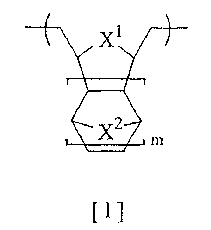
The resist composition contains a polymer comprising structural units of formula [I] in a backbone and having acid labile groups on side chains as a base resin and a photoacid generator.
Applications Claiming Priority (6)
| Application Number | Priority Date | Filing Date | Title |
|---|---|---|---|
| JP2001213015 | 2001-07-13 | ||
| JP2001213015 | 2001-07-13 | ||
| JP2001295653 | 2001-09-27 | ||
| JP2001295653 | 2001-09-27 | ||
| JP2002045588 | 2002-02-22 | ||
| JP2002045588 | 2002-02-22 |
Publications (3)
| Publication Number | Publication Date |
|---|---|
| EP1276012A2 EP1276012A2 (en) | 2003-01-15 |
| EP1276012A3 true EP1276012A3 (en) | 2003-03-19 |
| EP1276012B1 EP1276012B1 (en) | 2016-03-23 |
Family
ID=27347152
Family Applications (1)
| Application Number | Title | Priority Date | Filing Date |
|---|---|---|---|
| EP02254910.9A Expired - Lifetime EP1276012B1 (en) | 2001-07-13 | 2002-07-12 | Resist patterning process |
Country Status (4)
| Country | Link |
|---|---|
| US (1) | US6878508B2 (en) |
| EP (1) | EP1276012B1 (en) |
| KR (1) | KR100636067B1 (en) |
| TW (1) | TWI282036B (en) |
Families Citing this family (10)
| Publication number | Priority date | Publication date | Assignee | Title |
|---|---|---|---|---|
| KR100636068B1 (en) * | 2001-06-15 | 2006-10-19 | 신에쓰 가가꾸 고교 가부시끼가이샤 | Resist Composition and Patterning Process |
| KR100745064B1 (en) * | 2004-09-17 | 2007-08-01 | 주식회사 하이닉스반도체 | Top anti-reflective coating composition and method for pattern formation of semiconductor device using the same |
| TWI332122B (en) * | 2005-04-06 | 2010-10-21 | Shinetsu Chemical Co | Novel sulfonate salts and derivatives, photoacid generators, resist compositions and patterning process |
| US7396482B2 (en) * | 2005-10-28 | 2008-07-08 | Infineon Technologies Ag | Post exposure resist bake |
| EP1780199B1 (en) * | 2005-10-31 | 2012-02-01 | Shin-Etsu Chemical Co., Ltd. | Novel fluorohydroxyalkyl sulfonate salts and derivatives, photoacid generators, resist compositions, and patterning process |
| EP1780198B1 (en) * | 2005-10-31 | 2011-10-05 | Shin-Etsu Chemical Co., Ltd. | Novel fluorosulfonyloxyalkyl sulfonate salts and derivatives, photoacid generators, resist compositions, and patterning process |
| JP5124806B2 (en) * | 2006-06-27 | 2013-01-23 | 信越化学工業株式会社 | Photoacid generator, resist material and pattern forming method using the same |
| US8211984B2 (en) * | 2006-07-21 | 2012-07-03 | Mitsui Chemicals, Inc. | Ring-opening metathesis polymer, hydrogenated product thereof, method for preparing the same, and use thereof |
| KR101035742B1 (en) * | 2006-09-28 | 2011-05-20 | 신에쓰 가가꾸 고교 가부시끼가이샤 | Novel Photoacid Generators, Resist Compositions, and Patterning Process |
| US9104107B1 (en) | 2013-04-03 | 2015-08-11 | Western Digital (Fremont), Llc | DUV photoresist process |
Citations (5)
| Publication number | Priority date | Publication date | Assignee | Title |
|---|---|---|---|---|
| JPH11130844A (en) * | 1997-10-28 | 1999-05-18 | Mitsui Chem Inc | Acid-decomposable polymer and production thereof |
| JP2000109545A (en) * | 1998-06-29 | 2000-04-18 | Mitsui Chemicals Inc | Hydrogenated product of ring-opened metathesis polymer, its use and production thereof |
| EP1004568A2 (en) * | 1998-11-02 | 2000-05-31 | Shin-Etsu Chemical Co., Ltd. | Novel ester compounds, polymers, resist compositions and patterning process |
| US6207779B1 (en) * | 1998-06-30 | 2001-03-27 | Industrial Technology Research Institute | Ring-opened polymer |
| EP1099983A1 (en) * | 1999-11-12 | 2001-05-16 | Shin-Etsu Chemical Co., Ltd. | Chemically amplified positive resist composition and patterning method |
Family Cites Families (19)
| Publication number | Priority date | Publication date | Assignee | Title |
|---|---|---|---|---|
| JP2881969B2 (en) | 1990-06-05 | 1999-04-12 | 富士通株式会社 | Radiation-sensitive resist and pattern forming method |
| JP2898143B2 (en) | 1991-06-12 | 1999-05-31 | 三井化学株式会社 | Photosensitive liquid composition, photosensitive film and laminate |
| JPH05257285A (en) | 1992-03-12 | 1993-10-08 | Fujitsu Ltd | Radiosensitive material and formation of pattern using the same |
| JPH06342212A (en) | 1993-04-07 | 1994-12-13 | Matsushita Electric Ind Co Ltd | Resist for forming fine pattern and fine pattern forming method |
| JPH07333850A (en) | 1994-06-14 | 1995-12-22 | Sony Corp | Photosensitive composition |
| GB9509487D0 (en) * | 1995-05-10 | 1995-07-05 | Ici Plc | Micro relief element & preparation thereof |
| JPH09230595A (en) | 1996-02-26 | 1997-09-05 | Nippon Zeon Co Ltd | Resist composition and its utilization |
| KR100536824B1 (en) | 1996-03-07 | 2006-03-09 | 스미토모 베이클라이트 가부시키가이샤 | Photoresist compositions comprising polycyclic polymers with acid labile pendant groups |
| JP3691897B2 (en) | 1996-03-07 | 2005-09-07 | 富士通株式会社 | Resist material and resist pattern forming method |
| JP3785726B2 (en) | 1997-03-12 | 2006-06-14 | Jsr株式会社 | Radiation sensitive resin composition for semiconductor device manufacturing |
| JP3693477B2 (en) | 1997-10-28 | 2005-09-07 | 三井化学株式会社 | Hydrogenated product of ring-opening metathesis (co) polymer and process for producing the same |
| JP3678559B2 (en) | 1997-10-28 | 2005-08-03 | 三井化学株式会社 | Hydrogenated product of ring-opening metathesis (co) polymer and process for producing the same |
| JP3703277B2 (en) * | 1997-12-12 | 2005-10-05 | 三井化学株式会社 | Narrowly dispersible polymer having acid dissociable group and method for producing the same |
| KR100510448B1 (en) * | 1998-01-13 | 2005-10-21 | 삼성전자주식회사 | Manufacturing method of small photoresist pattern using thermal flow process for semiconductor device |
| JP4131062B2 (en) | 1998-09-25 | 2008-08-13 | 信越化学工業株式会社 | Novel lactone-containing compound, polymer compound, resist material, and pattern forming method |
| JP2000357544A (en) | 1999-04-16 | 2000-12-26 | Idemitsu Kosan Co Ltd | Coloring matter sensitizing type solar battery |
| JP3901401B2 (en) | 1999-07-13 | 2007-04-04 | 三井化学株式会社 | Positive photoresist composition and pattern forming method |
| TWI295284B (en) * | 2000-04-27 | 2008-04-01 | Shinetsu Chemical Co | |
| JP4365049B2 (en) * | 2000-10-20 | 2009-11-18 | 富士フイルム株式会社 | Pattern formation method using chemically amplified positive resist composition for thermal flow |
-
2002
- 2002-07-12 TW TW091115570A patent/TWI282036B/en not_active IP Right Cessation
- 2002-07-12 EP EP02254910.9A patent/EP1276012B1/en not_active Expired - Lifetime
- 2002-07-12 US US10/193,224 patent/US6878508B2/en not_active Expired - Lifetime
- 2002-07-12 KR KR1020020040550A patent/KR100636067B1/en active IP Right Grant
Patent Citations (6)
| Publication number | Priority date | Publication date | Assignee | Title |
|---|---|---|---|---|
| JPH11130844A (en) * | 1997-10-28 | 1999-05-18 | Mitsui Chem Inc | Acid-decomposable polymer and production thereof |
| JP2000109545A (en) * | 1998-06-29 | 2000-04-18 | Mitsui Chemicals Inc | Hydrogenated product of ring-opened metathesis polymer, its use and production thereof |
| US6372854B1 (en) * | 1998-06-29 | 2002-04-16 | Mitsui Chemicals, Inc. | Hydrogenated ring-opening metathesis polymer and its use and production |
| US6207779B1 (en) * | 1998-06-30 | 2001-03-27 | Industrial Technology Research Institute | Ring-opened polymer |
| EP1004568A2 (en) * | 1998-11-02 | 2000-05-31 | Shin-Etsu Chemical Co., Ltd. | Novel ester compounds, polymers, resist compositions and patterning process |
| EP1099983A1 (en) * | 1999-11-12 | 2001-05-16 | Shin-Etsu Chemical Co., Ltd. | Chemically amplified positive resist composition and patterning method |
Non-Patent Citations (1)
| Title |
|---|
| DATABASE WPI Section Ch Week 199930, Derwent World Patents Index; Class A17, AN 1999-352899, XP002217910 * |
Also Published As
| Publication number | Publication date |
|---|---|
| US20030108819A1 (en) | 2003-06-12 |
| KR20030032825A (en) | 2003-04-26 |
| US6878508B2 (en) | 2005-04-12 |
| EP1276012A2 (en) | 2003-01-15 |
| EP1276012B1 (en) | 2016-03-23 |
| KR100636067B1 (en) | 2006-10-20 |
| TWI282036B (en) | 2007-06-01 |
Similar Documents
| Publication | Publication Date | Title |
|---|---|---|
| KR101749601B1 (en) | Silicon-containing composition having sulfonamide group for forming resist underlayer film | |
| US4985342A (en) | Polysiloxane pattern-forming material with SiO4/2 units and pattern formation method using same | |
| KR101764259B1 (en) | Composition for forming silicon-containing resist underlayer film having sulfide bond | |
| KR101655251B1 (en) | Silicon-Containing Resist Underlayer Film-Forming Composition Containing Cyclic Amino Group | |
| US7867689B2 (en) | Method of use for photopatternable dielectric materials for BEOL applications | |
| JP4336310B2 (en) | Silicon-containing antireflection layer as hard mask layer and method for forming the same | |
| KR101847382B1 (en) | Silicon-containing resist underlayer-forming composition containing amic acid | |
| MY117818A (en) | Anti-reflective coating composition | |
| KR19990067915A (en) | Polymers and photoresist compositions for short wavelength imaging | |
| KR20060114293A (en) | Compositions and processes for immersion lithography | |
| KR20180118238A (en) | Composition for formation of resist underlayer film containing silicon having nitrogen-containing ring | |
| JP2004212946A (en) | PHOTORESIST CONTAINING Si POLYMER | |
| KR101729998B1 (en) | Compositions and processes for photolithography | |
| KR960022615A (en) | Photoresist composition | |
| KR101921513B1 (en) | Composition for forming resist underlayer films, containing silicon that bears diketone-structure-containing organic group | |
| CN102439069B (en) | Method and materials for reverse patterning | |
| KR20150097550A (en) | Composition for forming silicon-containing resist underlayer film having cyclic diester group | |
| EP1276012A3 (en) | Resist patterning process | |
| JP2003233190A (en) | Polymer with mixed photoacid-labile group and photoresist comprising the same | |
| KR101920649B1 (en) | Polymer-containing developer | |
| JP2004038142A (en) | Method for preparing polysiloxane and photoresist composition comprising same | |
| KR960011556A (en) | Water soluble film forming composition | |
| JP3014321B2 (en) | Chemically amplified photoresist composition | |
| KR20130084272A (en) | Photoresist compositions | |
| KR100557615B1 (en) | Photoresist composition for resist flow process |
Legal Events
| Date | Code | Title | Description |
|---|---|---|---|
| PUAI | Public reference made under article 153(3) epc to a published international application that has entered the european phase |
Free format text: ORIGINAL CODE: 0009012 |
|
| AK | Designated contracting states |
Kind code of ref document: A2 Designated state(s): AT BE BG CH CY CZ DE DK EE ES FI FR GB GR IE IT LI LU MC NL PT SE SK TR |
|
| AX | Request for extension of the european patent |
Free format text: AL;LT;LV;MK;RO;SI |
|
| PUAL | Search report despatched |
Free format text: ORIGINAL CODE: 0009013 |
|
| AK | Designated contracting states |
Kind code of ref document: A3 Designated state(s): AT BE BG CH CY CZ DE DK EE ES FI FR GB GR IE IT LI LU MC NL PT SE SK TR |
|
| AX | Request for extension of the european patent |
Extension state: AL LT LV MK RO SI |
|
| 17P | Request for examination filed |
Effective date: 20030626 |
|
| AKX | Designation fees paid |
Designated state(s): DE FR GB |
|
| 17Q | First examination report despatched |
Effective date: 20090209 |
|
| GRAP | Despatch of communication of intention to grant a patent |
Free format text: ORIGINAL CODE: EPIDOSNIGR1 |
|
| RIN1 | Information on inventor provided before grant (corrected) |
Inventor name: KOBAYASHI, TOMOHIRO Inventor name: WATANABE, SATOSHI |
|
| INTG | Intention to grant announced |
Effective date: 20151020 |
|
| GRAS | Grant fee paid |
Free format text: ORIGINAL CODE: EPIDOSNIGR3 |
|
| GRAA | (expected) grant |
Free format text: ORIGINAL CODE: 0009210 |
|
| AK | Designated contracting states |
Kind code of ref document: B1 Designated state(s): DE FR GB |
|
| REG | Reference to a national code |
Ref country code: GB Ref legal event code: FG4D |
|
| REG | Reference to a national code |
Ref country code: DE Ref legal event code: R096 Ref document number: 60247884 Country of ref document: DE |
|
| REG | Reference to a national code |
Ref country code: FR Ref legal event code: PLFP Year of fee payment: 15 |
|
| REG | Reference to a national code |
Ref country code: DE Ref legal event code: R097 Ref document number: 60247884 Country of ref document: DE |
|
| PLBE | No opposition filed within time limit |
Free format text: ORIGINAL CODE: 0009261 |
|
| STAA | Information on the status of an ep patent application or granted ep patent |
Free format text: STATUS: NO OPPOSITION FILED WITHIN TIME LIMIT |
|
| 26N | No opposition filed |
Effective date: 20170102 |
|
| GBPC | Gb: european patent ceased through non-payment of renewal fee |
Effective date: 20160712 |
|
| PG25 | Lapsed in a contracting state [announced via postgrant information from national office to epo] |
Ref country code: GB Free format text: LAPSE BECAUSE OF NON-PAYMENT OF DUE FEES Effective date: 20160712 |
|
| REG | Reference to a national code |
Ref country code: FR Ref legal event code: PLFP Year of fee payment: 16 |
|
| PGFP | Annual fee paid to national office [announced via postgrant information from national office to epo] |
Ref country code: FR Payment date: 20170613 Year of fee payment: 16 |
|
| PGFP | Annual fee paid to national office [announced via postgrant information from national office to epo] |
Ref country code: DE Payment date: 20170705 Year of fee payment: 16 |
|
| REG | Reference to a national code |
Ref country code: DE Ref legal event code: R119 Ref document number: 60247884 Country of ref document: DE |
|
| PG25 | Lapsed in a contracting state [announced via postgrant information from national office to epo] |
Ref country code: FR Free format text: LAPSE BECAUSE OF NON-PAYMENT OF DUE FEES Effective date: 20180731 Ref country code: DE Free format text: LAPSE BECAUSE OF NON-PAYMENT OF DUE FEES Effective date: 20190201 |