EP1274092A2 - Dispositif à stockage de données avec matrice de nanotubes comme sources d'électrons - Google Patents
Dispositif à stockage de données avec matrice de nanotubes comme sources d'électrons Download PDFInfo
- Publication number
- EP1274092A2 EP1274092A2 EP02254312A EP02254312A EP1274092A2 EP 1274092 A2 EP1274092 A2 EP 1274092A2 EP 02254312 A EP02254312 A EP 02254312A EP 02254312 A EP02254312 A EP 02254312A EP 1274092 A2 EP1274092 A2 EP 1274092A2
- Authority
- EP
- European Patent Office
- Prior art keywords
- nanotubes
- array
- electron sources
- data storage
- storage
- Prior art date
- Legal status (The legal status is an assumption and is not a legal conclusion. Google has not performed a legal analysis and makes no representation as to the accuracy of the status listed.)
- Withdrawn
Links
Images
Classifications
-
- G—PHYSICS
- G11—INFORMATION STORAGE
- G11C—STATIC STORES
- G11C13/00—Digital stores characterised by the use of storage elements not covered by groups G11C11/00, G11C23/00, or G11C25/00
- G11C13/02—Digital stores characterised by the use of storage elements not covered by groups G11C11/00, G11C23/00, or G11C25/00 using elements whose operation depends upon chemical change
- G11C13/025—Digital stores characterised by the use of storage elements not covered by groups G11C11/00, G11C23/00, or G11C25/00 using elements whose operation depends upon chemical change using fullerenes, e.g. C60, or nanotubes, e.g. carbon or silicon nanotubes
-
- B—PERFORMING OPERATIONS; TRANSPORTING
- B82—NANOTECHNOLOGY
- B82Y—SPECIFIC USES OR APPLICATIONS OF NANOSTRUCTURES; MEASUREMENT OR ANALYSIS OF NANOSTRUCTURES; MANUFACTURE OR TREATMENT OF NANOSTRUCTURES
- B82Y10/00—Nanotechnology for information processing, storage or transmission, e.g. quantum computing or single electron logic
-
- G—PHYSICS
- G11—INFORMATION STORAGE
- G11B—INFORMATION STORAGE BASED ON RELATIVE MOVEMENT BETWEEN RECORD CARRIER AND TRANSDUCER
- G11B20/00—Signal processing not specific to the method of recording or reproducing; Circuits therefor
- G11B20/10—Digital recording or reproducing
-
- G—PHYSICS
- G11—INFORMATION STORAGE
- G11B—INFORMATION STORAGE BASED ON RELATIVE MOVEMENT BETWEEN RECORD CARRIER AND TRANSDUCER
- G11B9/00—Recording or reproducing using a method not covered by one of the main groups G11B3/00 - G11B7/00; Record carriers therefor
- G11B9/12—Recording or reproducing using a method not covered by one of the main groups G11B3/00 - G11B7/00; Record carriers therefor using near-field interactions; Record carriers therefor
- G11B9/14—Recording or reproducing using a method not covered by one of the main groups G11B3/00 - G11B7/00; Record carriers therefor using near-field interactions; Record carriers therefor using microscopic probe means, i.e. recording or reproducing by means directly associated with the tip of a microscopic electrical probe as used in Scanning Tunneling Microscopy [STM] or Atomic Force Microscopy [AFM] for inducing physical or electrical perturbations in a recording medium; Record carriers or media specially adapted for such transducing of information
- G11B9/1409—Heads
-
- G—PHYSICS
- G11—INFORMATION STORAGE
- G11B—INFORMATION STORAGE BASED ON RELATIVE MOVEMENT BETWEEN RECORD CARRIER AND TRANSDUCER
- G11B9/00—Recording or reproducing using a method not covered by one of the main groups G11B3/00 - G11B7/00; Record carriers therefor
- G11B9/12—Recording or reproducing using a method not covered by one of the main groups G11B3/00 - G11B7/00; Record carriers therefor using near-field interactions; Record carriers therefor
- G11B9/14—Recording or reproducing using a method not covered by one of the main groups G11B3/00 - G11B7/00; Record carriers therefor using near-field interactions; Record carriers therefor using microscopic probe means, i.e. recording or reproducing by means directly associated with the tip of a microscopic electrical probe as used in Scanning Tunneling Microscopy [STM] or Atomic Force Microscopy [AFM] for inducing physical or electrical perturbations in a recording medium; Record carriers or media specially adapted for such transducing of information
- G11B9/1418—Disposition or mounting of heads or record carriers
-
- G—PHYSICS
- G11—INFORMATION STORAGE
- G11C—STATIC STORES
- G11C13/00—Digital stores characterised by the use of storage elements not covered by groups G11C11/00, G11C23/00, or G11C25/00
- G11C13/0002—Digital stores characterised by the use of storage elements not covered by groups G11C11/00, G11C23/00, or G11C25/00 using resistive RAM [RRAM] elements
- G11C13/0004—Digital stores characterised by the use of storage elements not covered by groups G11C11/00, G11C23/00, or G11C25/00 using resistive RAM [RRAM] elements comprising amorphous/crystalline phase transition cells
-
- G—PHYSICS
- G11—INFORMATION STORAGE
- G11C—STATIC STORES
- G11C2213/00—Indexing scheme relating to G11C13/00 for features not covered by this group
- G11C2213/70—Resistive array aspects
- G11C2213/81—Array wherein the array conductors, e.g. word lines, bit lines, are made of nanowires
-
- Y—GENERAL TAGGING OF NEW TECHNOLOGICAL DEVELOPMENTS; GENERAL TAGGING OF CROSS-SECTIONAL TECHNOLOGIES SPANNING OVER SEVERAL SECTIONS OF THE IPC; TECHNICAL SUBJECTS COVERED BY FORMER USPC CROSS-REFERENCE ART COLLECTIONS [XRACs] AND DIGESTS
- Y10—TECHNICAL SUBJECTS COVERED BY FORMER USPC
- Y10S—TECHNICAL SUBJECTS COVERED BY FORMER USPC CROSS-REFERENCE ART COLLECTIONS [XRACs] AND DIGESTS
- Y10S977/00—Nanotechnology
- Y10S977/902—Specified use of nanostructure
- Y10S977/932—Specified use of nanostructure for electronic or optoelectronic application
- Y10S977/943—Information storage or retrieval using nanostructure
Definitions
- the present invention relates generally to electron sources.
- the present invention also relates to data storage devices.
- the device includes multiple electron sources having electron emission surfaces that are proximate a storage medium. During write operations, the electron sources bombard the storage medium with relatively high intensity electron beams. During read operations, the electron sources bombard the storage medium with relatively low intensity electron beams.
- Size of storage bits in such a device may be reduced by decreasing the electron beam diameter. Reducing the storage bit size increases storage density and capacity, and it decreases storage cost.
- Spindt emitters could be used for generating focused electron beams in such a device.
- a Spindt emitter has a conical shape and emits an electron beam at the tip of its cone.
- the cone tip is made as sharp as possible to reduce operating voltage and achieve a small electron beam diameter.
- the present invention seeks to provide an improved data storage device.
- a data storage device includes nanotubes as electron sources.
- the embodiment of the ultra-high density data storage device shown includes a storage medium and an array of nanotubes that function as electron sources. More rugged than Spindt emitters, the nanotubes are not damaged if they make contact with the storage medium.
- the nanotubes have a higher electron beam directionality than Spindt emitters. The higher directionality results in an electron beam having increased focus and accuracy, which allows bit size to be reduced. Reducing the bit size increases storage density and reduces storage cost.
- the higher directionality also allows the tips of the nanotubes to be spaced further from the storage medium.
- the nanotubes also have a lower material transfer rate than Spindt emitters. The lower transfer rate increases the effective life of the electron sources.
- the storage medium 112 of the data storage device 110 includes a storage layer.
- the storage layer may be made of a phase-change material such as a chalcogenide-based phase change material.
- Local areas of the storage layer can be reversibly changed between at least two states by application of focused radiation with appropriate time dependence of power amplitude. For instance, local areas may be changed between amorphous and crystalline states, or they may be changed between different crystalline states.
- the state of an area may be changed from crystalline to amorphous by heating the area with a high intensity energy beam, enough to melt the phase change material, and then quickly decreasing the intensity of the beam to quench the area.
- Quenching a phase-change material causes it to cool rapidly into an amorphous state without time to nucleate and grow crystalline grains.
- the state of an area may be changed from amorphous to crystalline by using an energy beam to heat the phase-change material at a temperature sufficient to allow nucleation and growth of crystalline grains.
- the different states represent different logic values.
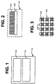
- the storage device 110 also includes an array 114 of nanotubes (e.g., carbon nanotubes, boron nitride nanotubes) that function as electron sources. Each nanotube emits an electron beam having appropriate time dependence of power amplitude to change a local storage area between amorphous and crystalline states or between different crystalline states. Tips of the nanotubes are proximate the storage layer. Electron optics may be used to focus the electron beams onto the storage medium 112.
- nanotubes e.g., carbon nanotubes, boron nitride nanotubes
- the array 114 of nanotube electron sources may be stationary relative to the storage medium 112. Thus, each nanotube tip may be stationed over a local storage area.
- micromovers (not shown) may be used to scan the array 114 of nanotubes along the surface of the storage layer during read and write operations. Exemplary micromovers are described in assignee's U.S. patent no. 5,986,381.
- Ruggedness and high directionality of the nanotubes allows a relaxation of the tolerances of the distance between the nanotube tips and the phase-change layer surface, the flatness of the phase-change layer surface, etc.
- the nanotubes 212 may be single-walled or double-walled, and they are defined by their diameter, length, conductivity, and chirality or twist.
- the nanotubes 212 are preferably elongated, as a higher aspect ratio provides better directionality.
- the nanotubes 212 may have an aspect ratio greater than 10:1.
- Carbon nanotubes, for example, are fullerene-related structures that are long, thin tubes of carbon. The carbon nanotubes are tightly bonded, which results in a low material transfer rate with the phase-change layer of the storage medium 112.
- the nanotubes 212 are formed on a substrate 214. Photolithographic or other masking techniques may be used to define where on the substrate 214 the nanotubes 212 are grown. Although only a single column often nanotubes 212 is shown in Figure 2, the array 114 may have any number of rows and columns. The array 114 may include hundreds or thousands of the nanotubes 212. Spacing between the nanotubes 212 will depend in part upon whether a micromover is used to scan the array 114 across the surface of the storage layer.
- word and bit lines 216 and 218 for addressing the nanotubes 212 are also formed on the substrate 214.
- the nanotubes 212 may be addressed simultaneously or in a multiplexed manner during read and write operations.
- a voltage is created between the selected nanotube 212 and the storage medium 112.
- the word and bit lines 216 and 218 are used to apply a voltage to the selected nanotube 212.
- a reference potential is applied to the storage medium 112, such that the selected nanotube 212 becomes a cathode and the storage medium 112 becomes an anode.
- the conductivity of the nanotubes 212 can be changed and the potentials can be varied to obtain electron beams of a desired time dependence of amplitude.
- the nanotubes 212 do not need an ultra-high vacuum to generate the electron beams.
- Read and write operations may be performed as described in Gibson et al. U.S. Patent No. 5,557,596, except that nanotubes are used instead of Spindt emitters.
- the nanotube electron sources are not limited to use in data storage devices.
- the nanotube electron sources may be used as electron emitters in lithographic applications.
Landscapes
- Engineering & Computer Science (AREA)
- Chemical & Material Sciences (AREA)
- Nanotechnology (AREA)
- Crystallography & Structural Chemistry (AREA)
- Signal Processing (AREA)
- Physics & Mathematics (AREA)
- Mathematical Physics (AREA)
- Theoretical Computer Science (AREA)
- Semiconductor Memories (AREA)
- Carbon And Carbon Compounds (AREA)
Applications Claiming Priority (2)
| Application Number | Priority Date | Filing Date | Title |
|---|---|---|---|
| US09/900,662 US6928042B2 (en) | 2001-07-06 | 2001-07-06 | Data storage device including nanotube electron sources |
| US900662 | 2001-07-06 |
Publications (2)
| Publication Number | Publication Date |
|---|---|
| EP1274092A2 true EP1274092A2 (fr) | 2003-01-08 |
| EP1274092A3 EP1274092A3 (fr) | 2003-10-15 |
Family
ID=25412893
Family Applications (1)
| Application Number | Title | Priority Date | Filing Date |
|---|---|---|---|
| EP02254312A Withdrawn EP1274092A3 (fr) | 2001-07-06 | 2002-06-20 | Dispositif à stockage de données avec matrice de nanotubes comme sources d'électrons |
Country Status (4)
| Country | Link |
|---|---|
| US (2) | US6928042B2 (fr) |
| EP (1) | EP1274092A3 (fr) |
| JP (1) | JP2003094400A (fr) |
| CN (1) | CN1396659A (fr) |
Cited By (4)
| Publication number | Priority date | Publication date | Assignee | Title |
|---|---|---|---|---|
| FR2862156A1 (fr) * | 2003-11-06 | 2005-05-13 | Commissariat Energie Atomique | Dispositif d'enregistrement de donnees a micro-pointes conductrices et procede de fabrication d'un tel dispositif |
| EP1744323A1 (fr) * | 2005-07-14 | 2007-01-17 | Qimonda AG | Cellule mémoire à changement de phase avec électrode de nanofil |
| WO2007030483A2 (fr) | 2005-09-06 | 2007-03-15 | Nantero, Inc. | Procede et systeme d'utilisation de tissus de nanotubes comme elements de chauffage ohmique pour memoires et autres applications |
| US7700934B2 (en) | 2004-09-27 | 2010-04-20 | Koninklijke Philips Electronics N.V. | Electric device with nanowires comprising a phase change material |
Families Citing this family (26)
| Publication number | Priority date | Publication date | Assignee | Title |
|---|---|---|---|---|
| US7260051B1 (en) * | 1998-12-18 | 2007-08-21 | Nanochip, Inc. | Molecular memory medium and molecular memory integrated circuit |
| US20020138301A1 (en) * | 2001-03-22 | 2002-09-26 | Thanos Karras | Integration of a portal into an application service provider data archive and/or web based viewer |
| US6982898B2 (en) | 2002-10-15 | 2006-01-03 | Nanochip, Inc. | Molecular memory integrated circuit utilizing non-vibrating cantilevers |
| US7233517B2 (en) * | 2002-10-15 | 2007-06-19 | Nanochip, Inc. | Atomic probes and media for high density data storage |
| US20060184843A1 (en) * | 2003-02-14 | 2006-08-17 | Oakley William S | Data recording using carbon nanotube electron sources |
| US8305861B2 (en) * | 2003-07-03 | 2012-11-06 | Oakley William S | Adaptive read and read-after-write for carbon nanotube recorders |
| WO2005013033A2 (fr) * | 2003-07-03 | 2005-02-10 | William Oakley | Groupement de tetes de nanotubes de carbone |
| US20050243660A1 (en) * | 2004-04-16 | 2005-11-03 | Rust Thomas F | Methods for erasing bit cells in a high density data storage device |
| US7620632B2 (en) * | 2004-06-30 | 2009-11-17 | Skyler Technology, Inc. | Method and/or system for performing tree matching |
| CN1300839C (zh) * | 2004-08-06 | 2007-02-14 | 中国科学院上海微系统与信息技术研究所 | 一种纳电子相变存储器的制备方法 |
| US20080204966A1 (en) * | 2004-09-21 | 2008-08-28 | The Johns Hopkins University | Controlled Transport and Assembly of Nanostructures |
| US7190539B1 (en) | 2004-12-29 | 2007-03-13 | Storage Technology Corporation | Magnetic recorder having carbon nanotubes embedded in anodic alumina for emitting electron beams to perform heat-assisted magnetic recording |
| US7463573B2 (en) * | 2005-06-24 | 2008-12-09 | Nanochip, Inc. | Patterned media for a high density data storage device |
| US20060291271A1 (en) * | 2005-06-24 | 2006-12-28 | Nanochip, Inc. | High density data storage devices having servo indicia formed in a patterned media |
| US20070041237A1 (en) * | 2005-07-08 | 2007-02-22 | Nanochip, Inc. | Media for writing highly resolved domains |
| US7367119B2 (en) * | 2005-06-24 | 2008-05-06 | Nanochip, Inc. | Method for forming a reinforced tip for a probe storage device |
| US20070008867A1 (en) * | 2005-07-08 | 2007-01-11 | Nanochip, Inc. | High density data storage devices with a lubricant layer comprised of a field of polymer chains |
| US20070008865A1 (en) * | 2005-07-08 | 2007-01-11 | Nanochip, Inc. | High density data storage devices with polarity-dependent memory switching media |
| US20070008866A1 (en) * | 2005-07-08 | 2007-01-11 | Nanochip, Inc. | Methods for writing and reading in a polarity-dependent memory switch media |
| US7309630B2 (en) * | 2005-07-08 | 2007-12-18 | Nanochip, Inc. | Method for forming patterned media for a high density data storage device |
| US20080001075A1 (en) * | 2006-06-15 | 2008-01-03 | Nanochip, Inc. | Memory stage for a probe storage device |
| US20080175033A1 (en) * | 2007-01-19 | 2008-07-24 | Nanochip, Inc. | Method and system for improving domain stability in a ferroelectric media |
| US20080233672A1 (en) * | 2007-03-20 | 2008-09-25 | Nanochip, Inc. | Method of integrating mems structures and cmos structures using oxide fusion bonding |
| CN101504948B (zh) * | 2008-02-05 | 2011-04-06 | 财团法人工业技术研究院 | 中空尖笔状结构与包含其的装置及其制造方法 |
| WO2012128763A1 (fr) * | 2011-03-23 | 2012-09-27 | Empire Technology Development Llc | Condensateur doté de nanotubes parallèles |
| US10225082B2 (en) | 2016-07-26 | 2019-03-05 | International Business Machines Corporation | Carbon nanotube physical entropy source |
Citations (5)
| Publication number | Priority date | Publication date | Assignee | Title |
|---|---|---|---|---|
| US5557596A (en) * | 1995-03-20 | 1996-09-17 | Gibson; Gary | Ultra-high density storage device |
| EP0945884A1 (fr) * | 1998-03-23 | 1999-09-29 | Nec Corporation | Dispositif d'émission à effet de champ avec une source d'électrons à nanotube de nitrure de bore |
| EP0951047A2 (fr) * | 1998-03-27 | 1999-10-20 | Canon Kabushiki Kaisha | Nanostructure, dispositif émetteur d'électrons, dispositif à nanotube de carbone, et leurs procédés de fabrication |
| US5986381A (en) * | 1997-03-14 | 1999-11-16 | Hewlett-Packard Company | Electrostatic actuator with spatially alternating voltage patterns |
| US6097138A (en) * | 1996-09-18 | 2000-08-01 | Kabushiki Kaisha Toshiba | Field emission cold-cathode device |
Family Cites Families (8)
| Publication number | Priority date | Publication date | Assignee | Title |
|---|---|---|---|---|
| DE4409850C2 (de) * | 1994-03-22 | 1999-05-12 | Fraunhofer Ges Forschung | Informationsspeichereinheit |
| US6498349B1 (en) * | 1997-02-05 | 2002-12-24 | Ut-Battelle | Electrostatically focused addressable field emission array chips (AFEA's) for high-speed massively parallel maskless digital E-beam direct write lithography and scanning electron microscopy |
| JP3403635B2 (ja) | 1998-03-26 | 2003-05-06 | 富士通株式会社 | 表示装置および該表示装置の駆動方法 |
| US6518570B1 (en) * | 1998-04-03 | 2003-02-11 | Brookhaven Science Associates | Sensing mode atomic force microscope |
| KR100398276B1 (ko) * | 1998-12-03 | 2003-09-19 | 다이켄카가쿠 코교 가부시키가이샤 | 전자장치의 표면신호조작용 프로우브 및 그 제조방법 |
| KR20010011136A (ko) * | 1999-07-26 | 2001-02-15 | 정선종 | 나노구조를 에미터로 사용한 삼극형 전계 방출 에미터의 구조및 그 제조방법 |
| US6519221B1 (en) | 1999-11-12 | 2003-02-11 | Massachusetts Institute Of Technology | High-density data storage using atomic force microscope |
| US6542400B2 (en) * | 2001-03-27 | 2003-04-01 | Hewlett-Packard Development Company Lp | Molecular memory systems and methods |
-
2001
- 2001-07-06 US US09/900,662 patent/US6928042B2/en not_active Expired - Lifetime
-
2002
- 2002-06-20 EP EP02254312A patent/EP1274092A3/fr not_active Withdrawn
- 2002-07-04 JP JP2002195692A patent/JP2003094400A/ja active Pending
- 2002-07-05 CN CN02141131A patent/CN1396659A/zh active Pending
-
2005
- 2005-05-25 US US11/136,882 patent/US7295503B2/en not_active Expired - Lifetime
Patent Citations (5)
| Publication number | Priority date | Publication date | Assignee | Title |
|---|---|---|---|---|
| US5557596A (en) * | 1995-03-20 | 1996-09-17 | Gibson; Gary | Ultra-high density storage device |
| US6097138A (en) * | 1996-09-18 | 2000-08-01 | Kabushiki Kaisha Toshiba | Field emission cold-cathode device |
| US5986381A (en) * | 1997-03-14 | 1999-11-16 | Hewlett-Packard Company | Electrostatic actuator with spatially alternating voltage patterns |
| EP0945884A1 (fr) * | 1998-03-23 | 1999-09-29 | Nec Corporation | Dispositif d'émission à effet de champ avec une source d'électrons à nanotube de nitrure de bore |
| EP0951047A2 (fr) * | 1998-03-27 | 1999-10-20 | Canon Kabushiki Kaisha | Nanostructure, dispositif émetteur d'électrons, dispositif à nanotube de carbone, et leurs procédés de fabrication |
Non-Patent Citations (2)
| Title |
|---|
| MURAKAMI H ET AL: "FIELD EMISSION FROM WELL-ALIGNED, PATTERNED, CARBON NANOTUBE EMITTERS" APPLIED PHYSICS LETTERS, AMERICAN INSTITUTE OF PHYSICS. NEW YORK, US, vol. 76, no. 13, 27 March 2000 (2000-03-27), pages 1776-1778, XP000950557 ISSN: 0003-6951 * |
| RUECKES T ET AL: "CARBON NANOTUBE-BASED NONVOLATILE RANDOM ACCESS MEMORY FOR MOLECULAR COMPUTING" SCIENCE, AMERICAN ASSOCIATION FOR THE ADVANCEMENT OF SCIENCE,, US, vol. 289, no. 5476, July 2000 (2000-07), pages 94-97, XP000925696 ISSN: 0036-8075 * |
Cited By (11)
| Publication number | Priority date | Publication date | Assignee | Title |
|---|---|---|---|---|
| FR2862156A1 (fr) * | 2003-11-06 | 2005-05-13 | Commissariat Energie Atomique | Dispositif d'enregistrement de donnees a micro-pointes conductrices et procede de fabrication d'un tel dispositif |
| WO2005048255A1 (fr) * | 2003-11-06 | 2005-05-26 | Commissariat A L'energie Atomique | Dispositif d'enregistrement de donnees a micro-pointes conductrices et procede de fabrication d'un tel dispositif |
| US7453789B2 (en) | 2003-11-06 | 2008-11-18 | Commissariat A L'energie Atomique | Data recording device with conducting microtips and production method thereof |
| US7700934B2 (en) | 2004-09-27 | 2010-04-20 | Koninklijke Philips Electronics N.V. | Electric device with nanowires comprising a phase change material |
| EP1744323A1 (fr) * | 2005-07-14 | 2007-01-17 | Qimonda AG | Cellule mémoire à changement de phase avec électrode de nanofil |
| US7420199B2 (en) | 2005-07-14 | 2008-09-02 | Infineon Technologies Ag | Resistivity changing memory cell having nanowire electrode |
| WO2007030483A2 (fr) | 2005-09-06 | 2007-03-15 | Nantero, Inc. | Procede et systeme d'utilisation de tissus de nanotubes comme elements de chauffage ohmique pour memoires et autres applications |
| EP1922743A2 (fr) * | 2005-09-06 | 2008-05-21 | Nantero, Inc. | Procede et systeme d'utilisation de tissus de nanotubes comme elements de chauffage ohmique pour memoires et autres applications |
| EP1922743A4 (fr) * | 2005-09-06 | 2008-10-29 | Nantero Inc | Procede et systeme d'utilisation de tissus de nanotubes comme elements de chauffage ohmique pour memoires et autres applications |
| AU2006287609B2 (en) * | 2005-09-06 | 2012-08-02 | Nantero, Inc. | Method and system of using nanotube fabrics as joule heating elements for memories and other applications |
| US8525143B2 (en) | 2005-09-06 | 2013-09-03 | Nantero Inc. | Method and system of using nanotube fabrics as joule heating elements for memories and other applications |
Also Published As
| Publication number | Publication date |
|---|---|
| US20030007443A1 (en) | 2003-01-09 |
| JP2003094400A (ja) | 2003-04-03 |
| US6928042B2 (en) | 2005-08-09 |
| CN1396659A (zh) | 2003-02-12 |
| US20050218322A1 (en) | 2005-10-06 |
| US7295503B2 (en) | 2007-11-13 |
| EP1274092A3 (fr) | 2003-10-15 |
Similar Documents
| Publication | Publication Date | Title |
|---|---|---|
| US7295503B2 (en) | Data storage device including nanotube electron sources | |
| JP4972000B2 (ja) | Afm型のデータ記憶装置 | |
| US7892063B2 (en) | Method of manufacturing tubular carbon molecule and tubular carbon molecule, method of manufacturing recording apparatus and recording apparatus, method of manufacturing field electron emission device and field electron emission device, and method of manufacturing display unit and display unit | |
| US6671778B2 (en) | Atomic resolution storage device configured as a redundant array of independent storage devices | |
| US6473388B1 (en) | Ultra-high density information storage device based on modulated cathodoconductivity | |
| JPH097240A (ja) | 記憶装置 | |
| US6735163B2 (en) | Ultra-high density storage device with resonant scanning micromover | |
| US6643248B2 (en) | Data storage device | |
| US6815875B2 (en) | Electron source having planar emission region and focusing structure | |
| US6911768B2 (en) | Tunneling emitter with nanohole openings | |
| JP2002326200A (ja) | 走査されるプローブと記憶媒体との間に電流を流すための方法 | |
| US20030081532A1 (en) | Supplementary energy sources for atomic resolution storage memory devices | |
| US7057997B2 (en) | Class of electron beam based data storage devices and methods of use thereof | |
| US20090059774A1 (en) | Method of storing a data bit in a phase change alloy material with an electron beam | |
| US6617597B2 (en) | Circuits and methods for electron-beam control | |
| US6930971B2 (en) | Ultra-high density storage device with electron beam steering | |
| JP4629314B2 (ja) | 原子分解能記憶デバイス | |
| US20050040383A1 (en) | Data storage device | |
| US6392915B1 (en) | Method of storing and retrieving binary information | |
| Kuo et al. | An ultra-compact electron-beam column | |
| US20040218508A1 (en) | Data cluster erasure |
Legal Events
| Date | Code | Title | Description |
|---|---|---|---|
| PUAI | Public reference made under article 153(3) epc to a published international application that has entered the european phase |
Free format text: ORIGINAL CODE: 0009012 |
|
| AK | Designated contracting states |
Kind code of ref document: A2 Designated state(s): AT BE CH CY DE DK ES FI FR GB GR IE IT LI LU MC NL PT SE TR |
|
| AX | Request for extension of the european patent |
Free format text: AL;LT;LV;MK;RO;SI |
|
| PUAL | Search report despatched |
Free format text: ORIGINAL CODE: 0009013 |
|
| AK | Designated contracting states |
Kind code of ref document: A3 Designated state(s): AT BE CH CY DE DK ES FI FR GB GR IE IT LI LU MC NL PT SE TR |
|
| AX | Request for extension of the european patent |
Extension state: AL LT LV MK RO SI |
|
| 17P | Request for examination filed |
Effective date: 20040405 |
|
| AKX | Designation fees paid |
Designated state(s): DE GB |
|
| STAA | Information on the status of an ep patent application or granted ep patent |
Free format text: STATUS: THE APPLICATION IS DEEMED TO BE WITHDRAWN |
|
| 18D | Application deemed to be withdrawn |
Effective date: 20060221 |