EP1274067A2 - Treiberschaltung - Google Patents
Treiberschaltung Download PDFInfo
- Publication number
- EP1274067A2 EP1274067A2 EP02014806A EP02014806A EP1274067A2 EP 1274067 A2 EP1274067 A2 EP 1274067A2 EP 02014806 A EP02014806 A EP 02014806A EP 02014806 A EP02014806 A EP 02014806A EP 1274067 A2 EP1274067 A2 EP 1274067A2
- Authority
- EP
- European Patent Office
- Prior art keywords
- switch
- voltage
- timing
- output terminal
- mos transistor
- Prior art date
- Legal status (The legal status is an assumption and is not a legal conclusion. Google has not performed a legal analysis and makes no representation as to the accuracy of the status listed.)
- Granted
Links
- 238000007599 discharging Methods 0.000 claims description 31
- 239000004973 liquid crystal related substance Substances 0.000 claims description 7
- 230000004913 activation Effects 0.000 claims description 5
- 230000009849 deactivation Effects 0.000 claims description 5
- 238000010586 diagram Methods 0.000 description 33
- 230000003068 static effect Effects 0.000 description 7
- 230000009471 action Effects 0.000 description 5
- 230000006870 function Effects 0.000 description 5
- 230000004048 modification Effects 0.000 description 4
- 238000012986 modification Methods 0.000 description 4
- 238000013459 approach Methods 0.000 description 3
- 230000003247 decreasing effect Effects 0.000 description 3
- 238000004088 simulation Methods 0.000 description 3
- 230000008859 change Effects 0.000 description 2
- 230000006872 improvement Effects 0.000 description 2
- 230000004044 response Effects 0.000 description 2
- 230000008901 benefit Effects 0.000 description 1
- 230000001413 cellular effect Effects 0.000 description 1
- 230000000052 comparative effect Effects 0.000 description 1
- 230000000694 effects Effects 0.000 description 1
- 238000004519 manufacturing process Methods 0.000 description 1
- 239000011159 matrix material Substances 0.000 description 1
- 238000000034 method Methods 0.000 description 1
- 230000003071 parasitic effect Effects 0.000 description 1
- 230000008569 process Effects 0.000 description 1
- 230000009467 reduction Effects 0.000 description 1
- 239000010409 thin film Substances 0.000 description 1
Images


Classifications
-
- G—PHYSICS
- G09—EDUCATION; CRYPTOGRAPHY; DISPLAY; ADVERTISING; SEALS
- G09G—ARRANGEMENTS OR CIRCUITS FOR CONTROL OF INDICATING DEVICES USING STATIC MEANS TO PRESENT VARIABLE INFORMATION
- G09G3/00—Control arrangements or circuits, of interest only in connection with visual indicators other than cathode-ray tubes
- G09G3/20—Control arrangements or circuits, of interest only in connection with visual indicators other than cathode-ray tubes for presentation of an assembly of a number of characters, e.g. a page, by composing the assembly by combination of individual elements arranged in a matrix no fixed position being assigned to or needed to be assigned to the individual characters or partial characters
- G09G3/2007—Display of intermediate tones
- G09G3/2011—Display of intermediate tones by amplitude modulation
-
- G—PHYSICS
- G09—EDUCATION; CRYPTOGRAPHY; DISPLAY; ADVERTISING; SEALS
- G09G—ARRANGEMENTS OR CIRCUITS FOR CONTROL OF INDICATING DEVICES USING STATIC MEANS TO PRESENT VARIABLE INFORMATION
- G09G3/00—Control arrangements or circuits, of interest only in connection with visual indicators other than cathode-ray tubes
- G09G3/20—Control arrangements or circuits, of interest only in connection with visual indicators other than cathode-ray tubes for presentation of an assembly of a number of characters, e.g. a page, by composing the assembly by combination of individual elements arranged in a matrix no fixed position being assigned to or needed to be assigned to the individual characters or partial characters
- G09G3/34—Control arrangements or circuits, of interest only in connection with visual indicators other than cathode-ray tubes for presentation of an assembly of a number of characters, e.g. a page, by composing the assembly by combination of individual elements arranged in a matrix no fixed position being assigned to or needed to be assigned to the individual characters or partial characters by control of light from an independent source
- G09G3/36—Control arrangements or circuits, of interest only in connection with visual indicators other than cathode-ray tubes for presentation of an assembly of a number of characters, e.g. a page, by composing the assembly by combination of individual elements arranged in a matrix no fixed position being assigned to or needed to be assigned to the individual characters or partial characters by control of light from an independent source using liquid crystals
- G09G3/3611—Control of matrices with row and column drivers
- G09G3/3685—Details of drivers for data electrodes
-
- H—ELECTRICITY
- H03—ELECTRONIC CIRCUITRY
- H03K—PULSE TECHNIQUE
- H03K17/00—Electronic switching or gating, i.e. not by contact-making and –breaking
- H03K17/16—Modifications for eliminating interference voltages or currents
- H03K17/161—Modifications for eliminating interference voltages or currents in field-effect transistor switches
- H03K17/162—Modifications for eliminating interference voltages or currents in field-effect transistor switches without feedback from the output circuit to the control circuit
- H03K17/163—Soft switching
- H03K17/164—Soft switching using parallel switching arrangements
-
- H—ELECTRICITY
- H03—ELECTRONIC CIRCUITRY
- H03K—PULSE TECHNIQUE
- H03K19/00—Logic circuits, i.e. having at least two inputs acting on one output; Inverting circuits
- H03K19/0175—Coupling arrangements; Interface arrangements
- H03K19/0185—Coupling arrangements; Interface arrangements using field effect transistors only
- H03K19/018557—Coupling arrangements; Impedance matching circuits
- H03K19/018571—Coupling arrangements; Impedance matching circuits of complementary type, e.g. CMOS
-
- G—PHYSICS
- G09—EDUCATION; CRYPTOGRAPHY; DISPLAY; ADVERTISING; SEALS
- G09G—ARRANGEMENTS OR CIRCUITS FOR CONTROL OF INDICATING DEVICES USING STATIC MEANS TO PRESENT VARIABLE INFORMATION
- G09G2310/00—Command of the display device
- G09G2310/02—Addressing, scanning or driving the display screen or processing steps related thereto
- G09G2310/0243—Details of the generation of driving signals
- G09G2310/0248—Precharge or discharge of column electrodes before or after applying exact column voltages
-
- G—PHYSICS
- G09—EDUCATION; CRYPTOGRAPHY; DISPLAY; ADVERTISING; SEALS
- G09G—ARRANGEMENTS OR CIRCUITS FOR CONTROL OF INDICATING DEVICES USING STATIC MEANS TO PRESENT VARIABLE INFORMATION
- G09G2310/00—Command of the display device
- G09G2310/02—Addressing, scanning or driving the display screen or processing steps related thereto
- G09G2310/0264—Details of driving circuits
- G09G2310/027—Details of drivers for data electrodes, the drivers handling digital grey scale data, e.g. use of D/A converters
-
- G—PHYSICS
- G09—EDUCATION; CRYPTOGRAPHY; DISPLAY; ADVERTISING; SEALS
- G09G—ARRANGEMENTS OR CIRCUITS FOR CONTROL OF INDICATING DEVICES USING STATIC MEANS TO PRESENT VARIABLE INFORMATION
- G09G2310/00—Command of the display device
- G09G2310/02—Addressing, scanning or driving the display screen or processing steps related thereto
- G09G2310/0264—Details of driving circuits
- G09G2310/0291—Details of output amplifiers or buffers arranged for use in a driving circuit
-
- G—PHYSICS
- G09—EDUCATION; CRYPTOGRAPHY; DISPLAY; ADVERTISING; SEALS
- G09G—ARRANGEMENTS OR CIRCUITS FOR CONTROL OF INDICATING DEVICES USING STATIC MEANS TO PRESENT VARIABLE INFORMATION
- G09G2330/00—Aspects of power supply; Aspects of display protection and defect management
- G09G2330/02—Details of power systems and of start or stop of display operation
- G09G2330/021—Power management, e.g. power saving
-
- H—ELECTRICITY
- H03—ELECTRONIC CIRCUITRY
- H03K—PULSE TECHNIQUE
- H03K2217/00—Indexing scheme related to electronic switching or gating, i.e. not by contact-making or -breaking covered by H03K17/00
- H03K2217/0036—Means reducing energy consumption
Definitions
- This invention relates to a driver circuit and, more particularly, to a driver circuit suited for driving a capacitive load.
- Fig. 13 is a diagram illustrating one example of the structure of a driver circuit in a liquid crystal display device disclosed in the specification of Japanese Patent Kokai Publication JP-A-11-119750.
- the driver circuit includes an N-channel MOS transistor 1011 whose source is connected to an input terminal T1 via a switch 1031 and whose gate and drain are tied together; a switch 1032 connected between the drain of the N-channel MOS transistor 1011 and a high-potential power supply VDD; an N-channel MOS transistor 1012 whose gate is connected in common with the gate of the N-channel MOS transistor 1011 (where the node at the point of connection is represented by V10) and whose drain is connected to the high-potential power supply VDD via a switch 1033; a P-channel MOS transistor 1021 whose source is connected to the input terminal T1 via a switch 1041 and whose gate and drain are tied together; a switch 1042 connected between the drain of the P-channel MOS transistor 1021 and the low-potential
- the source of the N-channel MOS transistor 1012 and the source of the P-channel MOS transistor 1022 are connected in common and to an output terminal T2.
- the driver circuit further includes preliminary charging/discharging means constituted by a switch 1044 connected between the output terminal T2 and the high-potential power supply VDD and a switch 1034 connected between the output terminal T2 and the low-potential power supply VSS.
- Fig. 14A is a timing chart illustrating the operation for controlling the switches in the conventional driver circuit of Fig. 13, and Fig. 14B is a diagram illustrating the voltage waveforms of the internal nodes V10, V20 and output voltage Vout of the conventional driver circuit of Fig. 13.
- the switches 1032 and 1034 are turned on to establish a precharging mode, as a result of which the output voltage Vout declines. Since the switches 1031 and 1032 are off and on, respectively, under these conditions, the bias voltage at the gates of the transistors 1011 and 1012 is the power supply voltage VDD.
- the switches 1031 and 1032 are turned on and off, respectively.
- the bias voltage changes to a voltage shifted from an input voltage Vin by an amount equivalent to a threshold value Vth1011 of the transistor 1011.
- the threshold value Vth of the transistor is represented by a potential for which the source is the reference.
- the switch 1034 is turned off, the precharging mode ends and the switch 1033 is turned on.
- the transistor 1012 acts as a source follower and therefore the output voltage Vout changes to a voltage shifted from the bias voltage V10 at the gate of the transistor 1012 by an amount equivalent to a threshold value Vth1012 of the N-channel MOS transistor 1012.
- the output voltage Vout is represented by the following equation:
- Vout ⁇ Vin will hold and the output voltage Vout will become approximately equal to the input voltage Vin.
- the switches 1042 and 1044 are turned on to establish the precharging mode, as a result of which the output voltage Vout rises. Since the switches 1041 and 1042 are off and on, respectively, under these conditions, the bias voltage at the gates of the transistors 1021, 1022 is the power supply voltage VSS.
- the switches 1041 and 1042 are turned on and off, respectively.
- the bias voltage changes to a voltage shifted from the input voltage Vin by an amount equivalent to a threshold value Vth1021 of the transistor 1021.
- the transistor 1022 acts as a source follower and therefore the output voltage Vout changes to a voltage shifted from the bias voltage V20 at the gate of the transistor 1022 by an amount equivalent to a threshold value Vth1022 of the transistor 1022.
- the output voltage Vout is represented by the following equation:
- Vth1021 ⁇ Vth1022 holds with regard to the threshold voltages of the P-channel MOS transistors 1021 and 1022, then Vout ⁇ Vin will hold and the output voltage Vout will become approximately equal to the input voltage Vin.
- the threshold voltage of a MOS transistor exhibits some variation.
- Vth1011 ⁇ Vth1012, Vth1021 ⁇ Vth1022 can be realized with comparative ease.
- the output voltage Vout can be made equal to the input voltage Vin and a data line DL can be driven with a high current supply capability owing to the source-follower action of the transistors.
- This driver circuit is such that the transistors 1012 and 1022 function as source followers and little power is consumed because current other than that necessary for charging and discharging does not flow.
- it is difficult to drive the output voltage Vout to a voltage equal to the input voltage Vin rapidly.
- the reason for this is that in a transistor source-follower operation, most actual transistors have such a characteristic that the current driving capability varies gently while gradually decreasing when the gate-source voltage approaches the threshold voltage, as a result of which an extended period of time is required for the gate-source voltage to reach the vicinity of the threshold voltage and stabilize in the source-follower operation.
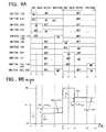
- Fig. 15 is a diagram illustrating a driver circuit described in the specification of Japanese Patent Kokai Publication JP-A-2000-338461 (see Fig. 9 in the same specification).
- this conventional driver circuit includes the N-channel MOS transistor 1011 whose source is connected to the input terminal T1 via the switch 1031 and whose gate and drain are tied together; a current source 1013 (current 111) connected between the drain of the N-channel MOS transistor 1011 and the high-potential power supply VDD; the N-channel MOS transistor 1012 whose gate is connected in common with the gate of the N-channel MOS transistor 1011 and whose drain is connected to the high-potential power supply VDD via the switch 1033; the switch 1032 connected between the common gates of the N-channel MOS transistors 1011 and 1012 and the high-potential power supply VDD; the P-channel MOS transistor 1021 whose source is connected to the input terminal T1 via the switch 1041 and whose gate and drain are tied together; a current source 1023 (current I21) connected between the drain of the P-channel MOS transistor 1021 and the low-potential power supply VSS; and the P-channel MOS transistor 1022 whose gate is connected in common
- the driver circuit further includes preliminary charging/discharging means constituted by the switch 1044 connected between the output terminal T2 and the high-potential power supply VDD and the switch 1034 connected between the output terminal T2 and the low-potential power supply VSS.
- the driver circuit further includes a switch 1046 and a current source 1025 (current 123) between the output terminal T2 and the high-potential power supply VDD, a switch 1036 and a current source 1015 (current I13) between the output terminal T2 and the low-potential power supply VSS, a switch 1045 and a current source 1024 (current I22) between the input terminal T1 and the high-potential power supply VDD, and a switch 1035 and a current source 1014 (current I12) between the input terminal T1 and the low-potential power supply VSS. It is assumed that a capacitive load (not shown) has been connected to the output terminal T2.
- Fig. 16A illustrates two output intervals, namely one output interval (times t0 to t3) in which a voltage of any level below voltage Vm is output, and a one output interval (times t0' to t3') in which a voltage of any level equal to or greater than voltage Vm is output.
- Fig. 16A illustrates two output intervals, namely one output interval (times t0 to t3) in which a voltage of any level below voltage Vm is output, and a one output interval (times t0' to t3') in which a voltage of any level equal to or greater than voltage Vm is output.
- Vgs1011(I11) is a gate voltage (gate-source voltage) with respect to the source when the drain current of the transistor 1011 is I11.
- the switches 1032 and 1034 are turned on and all of the switches 1042, 1044, 1041, 1045, 1043 and 1046 are turned off.
- the node V10 is precharged to the voltage VDD via the switch 1032.
- the switch 1032 is turned off and the switches 1031, 1035 are turned on, from which point the voltage V10 changes to a voltage shifted from the input voltage Vin by an amount equivalent to the gate-source voltage Vgs1011(I11) of the transistor 1011.
- the output voltage Vout is discharged to the voltage VSS if the switch 1034 is turned on at time t0.
- the output voltage Vout changes to a voltage shifted from the input voltage Vin by an amount equivalent to the gate-source voltage Vgs1012(I13) of the transistor 1012 owing to the source-follower operation of the transistor 1012.
- Vgs1011(I11) and Vgs1012(I13) are positive values and the currents I11 and I13 are controlled so as to make these two voltages equal, then the output voltage Vout will become equal to the input voltage Vin. Further, the output-voltage range becomes VSS ⁇ Vout ⁇ VDD-Vgs1012(I13)
- the switches 1042 and 1044 are turned on and the switches 1032, 1034, 1031, 1035, 1033 and 1036 are all turned off at time t0'.
- the voltage V20 is discharged to the voltage VSS via the switch 1042.
- the switch 1042 is turned off and the switches 1041 and 1045 are turned on, from which point the voltage V20 changes to a voltage shifted from the input voltage Vin by an amount equivalent to the gate-source voltage Vgs1021(I21) ( ⁇ 0) of the transistor 1021.
- the output voltage Vout is precharged to the voltage VDD if the switch 1044 is turned on at time t0'. If the switch 1044 is turned off and the switches 1043 and 1046 are turned on at time t2', then, from time t2' onward, the output voltage Vout changes to a voltage shifted from the voltage V20 by an amount equivalent to the gate-source voltage Vgs1022(I23) ( ⁇ 0) of the transistor 1022 owing to the source-follower operation of the transistor 1022.
- the voltage Vout stabilizes at If Vgs1021(I21) and Vgs1022(I23) are negative values and the currents I21 and I23 are controlled so as to make these two voltages equal, then the output voltage Vout will become equal to the input voltage Vin. Further, the output-voltage range becomes VSS-Vgs1022(I23) ⁇ Vout ⁇ VDD
- the switches 1031 and 1035 are ON from times t1 to t3, the switches 1033 and 1036 are on from times t2 to t3, the switches 1041 and 1045 are on from times t1' to t3' and the switches 1043 and 1046 are on from timings t2' to t3'.
- an operation maintaining current is passed substantially steadily and static power consumption occurs.
- the Inventor has found that there is room for improvement in this regard.
- Fig. 17 is a diagram illustrating a driver circuit described in the specification of Japanese Patent Kokai Publication JP-A-2000-338461 (see Fig. 12 in the same specification). The number of elements and the number of switching control signals are reduced over those of the arrangement shown in Fig. 15.
- this driver circuit is one in which the current control circuits 1014 and 1024 and the switches 1035 and 1045 have been eliminated from the arrangement of the driver circuit illustrated in Fig. 15 and to which a P-channel MOS transistor 1016 and an N-channel MOS transistor 1026 have been added anew.
- the P-channel MOS transistor 1016 has its source and drain connected to the gate (drain) and source, respectively, of the N-channel MOS transistor 1011, and has a voltage BIASP applied to its gate.
- the N-channel MOS transistor 1026 has its source and drain connected to the gate (drain) and source, respectively, of the P-channel MOS transistor 1021, and has a voltage BIASN applied to its gate.
- the voltage BIASP is supplied also to the gates of the P-channel MOS transistors 1013, 1025, and the voltage BIASN is supplied also to the gates of the N-channel MOS transistors 1015, 1023.
- the P-channel MOS transistor 1016 is made a transistor having a threshold voltage lower than that of the P-channel MOS transistor 1013 and a current supply capability sufficiently greater than that of the P-channel MOS transistor 1013 with respect to the same gate voltage.
- the N-channel MOS transistor 1026 also is made a transistor having a threshold voltage lower than that of the N-channel MOS transistor 1023 and a current supply capability sufficiently greater than that of the N-channel MOS transistor 1023 with respect to the same gate voltage.
- the circuit block consisting of the N-channel MOS transistor 1011 and P-channel MOS transistors 1013 and 1016 is represented by a circuit block 1010
- the circuit block consisting of the P-channel MOS transistor 1021 and N-channel MOS transistors 1023 and 1026 is represented by a circuit block 1020.
- the P-channel MOS transistor 1016 turns on when the input voltage Vin is in the vicinity of the power supply voltage VDD and the N-channel MOS transistor 1011 is about to turn off, and hence the transistor 1016 functions in such a manner that the current controlled by the current source 1013 flowing between the input terminal T1 and power supply VDD will not be cut off.
- the N-channel MOS transistor 1026 turns on when the input voltage Vin is in the vicinity of the power supply voltage VSS and the N-channel MOS transistor 1021 is about to turn off, and hence the transistor 1026 functions in such a manner that the current controlled by the current source 1023 flowing between the input terminal T1 and power supply VSS will not be cut off.
- the circuit block 1020 and switch 1041 can operate in a manner similar to that of the current source 1014 and switch 1035 in Fig. 15.
- the circuit block 1010 and switch 1031 can operate in a manner similar to that of the current source 1024 and switch 1045 in Fig. 15.
- the circuit of Fig. 17 can perform drive in a manner similar to the voltage waveforms shown in Fig. 16A.
- a driver circuit comprising a follower transistor arranged between an output terminal and a first power supply; a first control means for controlling activation and deactivation of the transistor; a current source arranged between the output terminal and a second power supply; a second control means for controlling activation and deactivation of the current source; and bias control means for supplying the transistor with an input bias voltage based upon an input signal voltage; wherein control is made such that said transistor is activated while said current source is deactivated at one timing in a data output interval, thereby causing said transistor to perform a follower operation, and then from a timing subsequent to the said one timing onward, both said transistor and said current source are activated to cause the output terminal voltage to be driven to a certain voltage, which is defined in conformity with the input signal voltage.
- a driver circuit in accordance with another aspect of the present invention comprises a follower transistor and a first switch connected serially between an output terminal and a first power supply; a first current source and a second switch connected serially between the output terminal and a second power supply; and bias control means for supplying the follower transistor with an input bias voltage based upon an input signal voltage; wherein the first switch is turned on at one timing in a data output interval, thereby causing the transistor to perform a follower operation to drive the output terminal voltage to the vicinity of a certain voltage defined in conformity with the input signal voltage; the second switch is turned on at a timing subsequent to the one timing, thereby placing both the first and second switches in the ON state; and the output terminal voltage is driven to the certain voltage, which is defined in conformity with the input signal voltage, from the subsequent timing onward.
- a driver circuit comprising a source-follower first MOS transistor of first conductivity type and a first switch connected serially between an output terminal and a high-potential power supply; a first current source and a second switch connected serially between the output terminal and a low-potential power supply; first gate bias control means for supplying the first MOS transistor with a gate bias voltage based upon an input signal voltage; and means for turning on the first switch at one timing in a data output interval, thereby causing the first MOS transistor to perform a source-follower operation to drive the output terminal voltage to the vicinity of a certain voltage defined in conformity with the input signal voltage, and turning on the second switch at a timing subsequent to the one timing, thereby placing both the first and second switches in the ON state; wherein the output terminal voltage is driven to the certain voltage, which is defined in conformity with the input signal voltage, from the subsequent timing onward, which is for controlling drain current of the first MOS transistor.
- a driver circuit comprises a source-follower second MOS transistor of second conductivity type and a third switch connected serially between an output terminal and a low-potential power supply; a second current source and a fourth switch connected serially between the output terminal and a high-potential power supply; second gate bias control means for supplying the second MOS transistor with a gate bias voltage based upon an input signal voltage; and means for turning on the third switch at one timing in a data output interval, thereby causing the second MOS transistor to perform a source-follower operation to drive the output terminal voltage to the vicinity of a certain voltage defined in conformity with the input signal voltage, and turning on the fourth switch at a timing subsequent to the one timing, thereby placing both the third and fourth switches in the ON state; wherein the output terminal voltage is driven to the certain voltage, which is defined in conformity with the input signal voltage, from the subsequent timing onward, which is for controlling drain current of the second MOS transistor.
- the first gate bias control means includes a third MOS transistor of first conductivity type having a drain and gate connected in common with a gate of the first MOS transistor and a source connected to the input terminal via a fifth switch; a third current source and a sixth switch connected serially between the drain of the third MOS transistor and the high-potential power supply; a fourth current source and a seventh switch connected serially between a connection node of the input terminal and fifth switch and the low-potential power supply; and an eighth switch connected between a common connection node of the gates of the first and third MOS transistors and the high-potential power supply.
- the second gate bias control means includes a fourth MOS transistor of second conductivity type having a drain and gate connected in common with a gate of the second MOS transistor and a source connected to the input terminal via a ninth switch; a fifth current source and a tenth switch connected serially between the drain of the fourth MOS transistor and the low-potential power supply; a sixth current source and an 11th switch connected serially between a connection node of the input terminal and ninth switch and the high-potential power supply; and a 12th switch connected between a common connection node of the gates of the second and fourth MOS transistors and the low-potential power supply.
- Fig.1 is a diagram illustrating the basic structure of a driver circuit according to an embodiment of the present invention.
- the driver circuit comprises: a follower transistor (111) and a switch (131) connected serially between an output terminal (T2) and a power supply (VDD); a current source (113) and a switch (132) connected serially between the output terminal (T2) and a power supply (VSS); and bias control means (11) for supplying the transistor (111) with a bias voltage based upon an input signal voltage.
- the switch (131) is turned on at one timing in a data output interval, thereby causing the transistor (111) to perform a follower operation to drive output terminal voltage Vout to the vicinity of a certain voltage defined in conformity with input signal voltage Vin.
- the switch (132) is turned on (switch 131 also is on) at a timing subsequent to the one timing, and the output terminal voltage is driven to the certain voltage, which is defined in conformity with the input signal voltage Vin, from the subsequent timing onward.
- a driver circuit comprises: a follower transistor (121) and a switch (141) connected serially between an output terminal (T2) and a power supply (VSS); a current source (123) and a switch (142) connected serially between the output terminal (T2) and a power supply (VDD); and bias control means (12) for supplying the transistor (121) with a bias voltage based upon an input signal voltage.
- the switch (141) is turned on at one timing in a data output interval, thereby causing the transistor (121) to perform a follower operation to drive output terminal voltage Vout to the vicinity of a certain voltage defined in conformity with input signal voltage Vin.
- the switch (142) is turned on (switch 141 also is on) at a timing subsequent to the one timing, and the output terminal voltage is driven to the certain voltage, which is defined in conformity with the input signal voltage Vin, from the subsequent timing onward.
- a driver circuit comprises: a source-follower first transistor (111) of first conductivity type and a first switch (131) connected serially between a high-potential power supply (VDD) and an output terminal (T2); a first current source (113) and a second switch (132) connected serially between a low-potential power supply (VSS) and the output terminal (T2); a source-follower transistor (121) of second conductivity type and a third switch (141) connected serially between the output terminal (T2) and the low-potential power supply (VSS); a second current source (123) and a fourth switch (142) connected serially between the high-potential power supply (VDD) and the output terminal (T2); first gate bias control means (11), to which input signal voltage Vin from the input terminal (T1) is applied, for controlling bias voltage of the gate of the transistor (111) of first conductivity type; second gate bias control means (12), to which the input signal voltage Vin is applied, for controlling bias voltage of the gate
- the first gate bias control means (11) is made capable of supplying a bias voltage such that a voltage difference between the bias voltage supplied to the gate of the transistor (111) of the first conductivity type and a desired voltage defined in conformity with the input signal voltage Vin will become equal to the gate-source voltage that prevails when current controlled by the first current source (113) flows into the transistor (111) of the first conductivity type.
- the second gate bias control means (12) is made capable of supplying a bias voltage such that a voltage difference between the bias voltage supplied to the gate of the transistor (121) of the second conductivity type and a desired voltage defined in conformity with the input signal voltage Vin will become equal to the gate-source voltage that prevails when current controlled by the second current source (123) flows into the transistor (121) of the second conductivity type.
- an interval for controlling the drain current of the transistors (111, 121) and an interval for cutting off this current are provided to reduce power consumption in the cut-off interval.
- the first to fourth switches (131, 132, 141 and 142) are all turned off in a first timing interval (times t0 to t1 in Fig. 2), as a result of which the output terminal (T2) is pre-discharged to a voltage below the desired voltage by the preliminary charging/discharging means (13).
- a second timing interval times t1 to t2 in Fig. 2
- preliminary discharge is halted and the first switch (131) is turned on.
- the source-follower operation of the transistor (111) of first conductivity type is enabled and the output terminal (T2) can be pulled up to the vicinity of a desired voltage.
- static power consumption does not occur because no feed-through current flows from the high-potential power supply (VDD) to the low-potential power supply (VSS).
- VDD high-potential power supply
- VSS low-potential power supply
- the transistor (111) of first conductivity type may have such a characteristic that the current driving capability varies gently while gradually decreasing when the gate-source voltage of this transistor is in the vicinity of the threshold voltage.
- a third timing interval times t2 to t3 in Fig. 2
- the second switch (132) is turned on while the first switch (131) is left in the ON state.
- the source-follower operation of the transistor (111) of the first conductivity type stabilizes rapidly when the drain current of the transistor (111) of the first conductivity type becomes equal to the current controlled by the first current source (113), and the output terminal (T2) can be driven to the desired voltage at high speed.
- the first to fourth switches are all turned off in a first timing interval (times t0' to t1' in Fig. 2), as a result of which the output terminal (T2) is precharged to a voltage greater than the desired voltage.
- a second timing interval times t1' to t2' in Fig. 2
- preliminary charging is halted and the third switch (141) is turned on.
- the source-follower operation of the transistor (121) of second conductivity type is enabled and the output terminal (T2) can be pulled down to the vicinity of a desired voltage.
- no feed-through current flows from the high-potential power supply (VDD) to the low-potential power supply (VSS).
- VDD high-potential power supply
- VSS low-potential power supply
- the transistor (121) of second conductivity type may have such a characteristic that the current driving capability varies gently while gradually decreasing when the gate-source voltage of this transistor is in the vicinity of the threshold voltage.
- the fourth switch (142) is turned on while the third switch (141) is left in the ON state.
- the source-follower operation of the transistor (121) of the second conductivity type stabilizes rapidly when the drain current of the transistor (121) of the second conductivity type becomes equal to the current controlled by the second current source (123), and the output terminal (T2) can be driven to the desired voltage at high speed. terminal (T2) can be driven to the desired voltage at high speed.
- the source-follower operation of the transistors (111 and 121) is carried out even in the cut-off interval in which the switches (132 and 142) are turned off.
- drive up to the vicinity of the desired voltage can be achieved without any static power consumption.
- drive up to the desired voltage can be achieved with high voltage precision.
- power consumption can be reduced in comparison with the conventional driver circuits, described above with reference to Figs. 15 and 17, etc., while a high output precision is maintained.
- the currents controlled by the first current source (113) and second current source (123) should be levels at which the output terminal (T2) can be driven to the desired voltage rapidly by the source-follower operation of the transistor (111) of the first conductivity type and transistor (121) of the second conductivity type in the third timing interval (times t2 to t3 and t2' to t3' in Fig. 2). This will make it possible to reduce power consumption by holding current to a low level.
- the first gate bias control means (11), as shown in Fig. 3, preferably includes a third MOS transistor (112) of first conductivity type having a drain and gate connected in common with a gate of the first MOS transistor (111) and a source connected to the input terminal via a fifth switch (133); a third current source (114) and a sixth switch (134) connected serially between the drain of the third MOS transistor (112) and the a high-potential power supply (VDD); a fourth current source (115) and a seventh switch (135) connected serially between a connection node of the input terminal (T1) and fifth switch (133) and a low-potential power supply (VSS); and an eighth switch (136) connected between a common connection node of the gates of the first and third MOS transistors (111 and 112) and the high-potential power supply (VDD).
- a third MOS transistor (112) of first conductivity type having a drain and gate connected in common with a gate of the first MOS transistor (111) and a source
- the second gate bias control means (12) preferably includes a fourth MOS transistor (122) of second conductivity type having a drain and gate connected in common with a gate of the second MOS transistor (121) and a source connected to the input terminal via a ninth switch (143); a fifth current source (124) and a tenth switch (144) connected serially between the drain of the fourth MOS transistor and the low-potential power supply (VSS); a sixth current source (125) and an 11th switch (145) connected serially between a connection node of the input terminal (T1) and ninth switch (143) and the high-potential power supply (VDD); and a 12th switch (146) connected between a common connection node of the gates of the second and fourth MOS transistors (121 and 122) and the low-potential power supply (VSS).
- a fourth MOS transistor (122) of second conductivity type having a drain and gate connected in common with a gate of the second MOS transistor (121) and a source connected to the input terminal via a ninth switch (143); a fifth
- the data output interval in which the input signal voltage Vin is at the low potential comprises four intervals, as shown in Fig. 4A.
- a first timing interval times t0 to t1
- the output terminal (T2) is pre-discharged to a voltage below a desired voltage
- the eighth switch (136) is turned on and the remaining first to seventh and ninth to 12th switches are already off.
- the eighth switch (136) By turning on the eighth switch (136), the common gate of the first MOS transistor (111) and third MOS transistor (112) of the first conductivity type are charged to the voltage of the high-potential power supply (VDD).
- the output terminal (T2) continues to be pre-discharged, the eighth switch (136) is turned off and the fifth switch (133) is turned on.
- the gate bias voltage of the first MOS transistor (111) becomes a voltage shifted from the input signal voltage Vin by an amount equivalent to the threshold voltage of the third MOS transistor (112) owing to the action of the third MOS transistor (112).
- a third timing interval times t2 to t3
- the preliminary discharging of the output terminal (T2) is halted, the first switch (131) is turned on and the fifth switch (133) is already on.
- the source-follower operation of the first MOS transistor (111) of first conductivity type is enabled and the output terminal (T2) can be pulled up to a voltage shifted from the gate bias voltage by an amount equivalent to the threshold voltage of first MOS transistor (111).
- a fourth timing interval times t3 to t4
- the second switch (132) is turned on, the first switch (131) and the fifth switch (133) are already on, and the sixth switch (134) and seventh switch (135) are turned on.
- the current controlled by the third current source (114) flows into the third MOS transistor, whereby the gate-source voltage of the third MOS transistor is decided and the gate bias voltage of the third MOS transistor becomes a voltage shifted from the input signal voltage Vin by an amount equivalent to the gate-source voltage of the third MOS transistor (112).
- the source-follower operation of the first MOS transistor (111) rapidly pulls the output terminal (T2) up to a voltage shifted from the gate bias voltage by an amount equivalent to the gate-source voltage of the first MOS transistor (111). Stability is quickly achieved.
- the gate-source voltage of the first MOS transistor (111) at this time is decided by current I13 controlled by the first current source (113). Accordingly, a desired voltage conforming to the input signal voltage Vin can be output to the output terminal (T2) by setting the currents of the first current source (113) and third current source (114) in optimum fashion.
- the data output interval in which the input signal voltage Vin is at the high potential comprises four intervals, as shown in Fig. 4B.
- a first timing interval times t0' to t1'
- the output terminal (T2) is precharged to a voltage above a desired voltage
- the 12th switch (146) is turned on and the remaining first to 11th switches are already off.
- the common gate of the second MOS transistor (121) and fourth MOS transistor (122) of the second conductivity type are discharged to the voltage of the low-potential power supply (VSS).
- the output terminal (T2) continues to be precharged, the 12th switch (146) is turned off and the ninth switch (143) is turned on.
- the gate bias voltage of the second MOS transistor (121) becomes a voltage shifted from the input signal voltage Vin by an amount equivalent to the threshold voltage of the fourth MOS transistor (122) owing to the action of the fourth MOS transistor (122).
- a third timing interval times t2' to t3'
- the preliminary charging of the output terminal (T2) is halted, the third switch (141) is turned on and the ninth switch (143) is already on.
- the source-follower operation of the second MOS transistor (121) of second conductivity type is enabled and the output terminal (T2) can be pulled down to a voltage shifted from the gate bias voltage by an amount equivalent to the threshold voltage of second third MOS transistor (121).
- the fourth switch (142) is turned on, the third switch (141) and the ninth switch (143) are already on, and the 10th switch (144) and 11th switch (145) are turned on.
- the current controlled by the fifth current source (124) flows into the fourth MOS transistor (122), whereby the gate-source voltage of the fourth MOS transistor (122) is decided and the gate bias voltage of the second MOS transistor (121) becomes a voltage shifted from the input signal voltage Vin by an amount equivalent to the gate-source voltage of the fourth MOS transistor (122).
- the source-follower operation of the second MOS transistor (121) rapidly pulls the output terminal (T2) down to a voltage shifted from the gate bias voltage by an amount equivalent to the gate-source voltage of the second MOS transistor (121). Stability is quickly achieved.
- the gate-source voltage of the second MOS transistor (121) at this time is decided by current I23 controlled by the second current source (123). Accordingly, a desired voltage conforming to the input signal voltage Vin can be output to the output terminal (T2) by setting the currents of the second current source (123) and fifth current source (124) in optimum fashion.
- the currents of the second current source (123) and fifth current source (124) are set so as to equalize the gate-source voltages of the second MOS transistor (121) and fourth MOS transistor (122), then a voltage equal to the input signal voltage Vin can be output to the output terminal (T2).
- the fourth current source (115) is controlled to a current equal to that of the third current source (114)
- the sixth current source (125) is controlled to a current equal to that of the fifth current source (124).
- a gate bias voltage for the first MOS transistor (111) and second MOS transistor (121) can be provided rapidly with respect to the input signal voltage Vin in the fourth timing interval (times t3 to t4 and times t3' to t4' in Figs. 4A and 4B). Furthermore, if a sufficient current can be supplied from the input terminal (T1), a gate bias voltage for the first MOS transistor (111) and second MOS transistor (121) can be provided rapidly with respect to the input signal voltage Vin and, hence, the fourth current source (115), the seventh switch (135), the sixth current source (125) and the 11th switch (145) need not be provided.
- the preliminary charging or discharging of the output terminal (T2) is performed in both the first timing interval (times t0 to t1 and times t0' to t1' in Figs. 4A and 4B) and second timing interval (times t1 to t2 and times t1' to t2' in Figs. 4A and 4B).
- the preliminary charging or discharging may be performed in either the first timing interval or the second timing interval.
- the driver circuit according to the embodiment of the present invention reduces power consumption significantly in comparison with the driver circuits shown in Figs. 15 and 17 and produces a voltage output of higher precision.
- the driver circuit therefore is ideal for application to a data-line driver circuit (100 in Fig. 12) in an active matrix display device and is particularly well suited for application to a liquid crystal display device of a battery-driven portable terminal.
- Fig. 1 is a diagram illustrating the structure of a driver circuit according to an embodiment of the present invention.
- the driver circuit according to this embodiment is one having a follower-type output transistor for producing a voltage, which is equal to an input signal voltage Vin, as an output voltage Vout.
- the driver circuit comprises: an N-channel MOS transistor 111 having a drain connected to a high-potential power supply VDD via a switch 131 and a source connected to an output terminal T2; a P-channel MOS transistor 121 having a drain connected to a low-potential power supply VSS via a switch 141 and a source connected to the output terminal T2; a current source 113 and a switch 132 connected serially between the output terminal T2 and the low-potential power supply VSS; a current source 123 and a switch 142 connected serially between the output terminal T2 and the high-potential power supply VDD; gate bias control means 11, 12, which receive the input signal voltage Vin, for controlling gate voltage in such a manner that output voltage Vout will become equal to the input voltage Vin; and preliminary charging/discharging means 13 for precharging or pre-discharging the output terminal T2 in accordance with the input signal voltage Vin.
- the bias control means 11 is capable of supplying a bias voltage such that a voltage difference between the bias voltage supplied to the gate of the transistor 111 and the input signal voltage Vin will become equal to the gate-source voltage that prevails when current controlled by the current source 113 flows into the transistor 111.
- the second gate bias control means 12 is capable of supplying a bias voltage such that a voltage difference between the bias voltage supplied to the gate of the transistor 121 and the input voltage Vin will become equal to the gate-source voltage that prevails when current controlled by the current source 123 flows into the transistor 121.
- the order of the switch 132 and current source 113 connected serially between the output terminal T2 and power supply VSS may be reversed, as well as the order of the switch 142 and current source 143 connected serially between the output terminal T2 and power supply VDD. Further, an arrangement may be adopted in which the drain of the transistor 111 is connected to the power supply VDD and the switch 131 is connected between the source of this transistor and the output terminal T2, or an arrangement may be adopted in which the drain of the transistor 121 is connected to the power supply VSS and the switch 141 is connected between the source of this transistor and the output terminal T2.
- Fig. 2 is a diagram illustrating the operation for controlling the switches in the driver circuit shown in Fig. 2. This is an example in which one data output interval comprises three drive intervals. The control operation according to this embodiment of the invention will be described with reference to Figs. 1 and 2.
- the preliminary charging/discharging means 13 pre-discharges the output terminal T2 to a voltage below the input signal voltage Vin and the switches 131, 132, 141 and 142 are all off in the interval t0 to t1.
- the switch 132 is turned on, so that both switches 131 and 132 are on.
- the current controlled by the current source 113 flows into the transistor 111, whereby the gate-source voltage of the transistor 111 is determined rapidly to realize a highly precise output.
- the preliminary charging/discharging means 13 precharges the output terminal T2 to a voltage above the input signal voltage Vin and the switches 131, 132, 141 and 142 are all off in the interval t0' to t1'.
- switches 131 and 141 are provided for exercising control to stop or deactivate the operation of transistors 111 and 121 respectively and hence such a circuit configuration may well be adopted in which switches 131 and 141 are replaced by any circuit means, which are provided for example in gate-bias control means 11 and 12, for controlling changeover between activation and deactivation of transistors 111 and 121 respectively. With this circuit configuration, switches 131 and 141 may well be omitted.
- This embodiment is such that if one data output interval is comparatively long, as in a data-line driver circuit for a low-resolution panel such as a TFT (thin-film transistor) LCD (liquid crystal display device) for a cellular telephone, the interval t0 to t2 and the interval t0' to t2' are lengthened and settling time, which finally determines pixel write voltage in one data output interval, is allocated to interval t2 to t3 and interval t2' to t3', thereby making it possible to achieve a highly precise pixel write voltage and to reduce power consumption by a wide margin.
- a data-line driver circuit for a low-resolution panel such as a TFT (thin-film transistor) LCD (liquid crystal display device) for a cellular telephone
- the interval t0 to t2 and the interval t0' to t2' are lengthened and settling time, which finally determines pixel write voltage in one data output interval, is allocated to interval t2 to t3 and interval
- Fig. 3 is a diagram showing an example of the structures of the bias control means 11 and 12 in the driver circuit of the embodiment shown in Fig. 1.
- the bias control means 11 includes an N-channel MOS transistor 112 having a drain and gate connected in common with the gate of the transistor 111 and a source connected to the input terminal T1 via a switch 133; a current source 114 having one end connected to the drain of the N-channel transistor 112; a switch 134 connected between the other end of the current source 114 and the power supply VDD; a current source 115 having one end connected to the node of the input terminal T1 and switch 133; a switch 135 connected between the other end of the current source 115 and the power supply VSS; and a switch 136 connected between a common connection node of the gates of the N-channel MOS transistors 111, 112 and the power supply VDD.
- the bias control means 12 includes a P-channel MOS transistor 122 having a drain and gate connected in common with the gate of the transistor 121 and a source connected to the input terminal T1 via a switch 143; a current source 124 having one end connected to the drain of the P-channel transistor 122; a switch 144 connected between the other end of the current source 124 and the power supply VSS; a current source 125 having one end connected to the node of the input terminal T1 and switch 143; a switch 145 connected between the other end of the current source 125 and the power supply VDD; and a switch 146 connected between a common connection node of the gates of the P-channel MOS transistors 121 and 122 and the power supply VSS.
- the preliminary charging/discharging means 13 the switches 131, 132, 141 and 142, the current sources 113 and 123 and the transistors 111 and 121 are arranged in a manner similar to that shown in Fig. 1.
- Figs. 4A and 4B are diagrams in which the operation for controlling the switches of the driver circuits shown in Fig. 3 is summarized in table form. Specifically, the example of the control operation depicted in Figs. 4A and 4B is such that one data output interval comprises four drive intervals. Figs. 4A and 4B illustrate the on and off states of the switches in one data interval of low potential level and one data interval of high potential level, respectively, in table form. The operation of the bias control means 11 and 12 will be described with reference to Figs. 4A and 4B.
- the switch 136 is turned off and the switch 133 is turned on, whereupon the gates of the transistors 111 and 112 change in such a manner that the gate-source voltage of the transistor 112 attains a threshold voltage.
- the switch 131 is turned on so that the transistor 111 is made to perform a source-follower operation, whereupon the transistor 111 also pulls up the voltage of the pre-discharged output terminal T2 so that the gate-source voltage changes to a voltage in the vicinity of the threshold voltage.
- the output voltage Vout therefore, is driven to the vicinity of Vin.
- the switches 132, 133, 134 and 135 are turned on.
- the output voltage Vout will be driven to a voltage equal to Vin rapidly if the current sources 113, 114 and 115 have been set so as to equalize the gate-source voltages of the transistors 111 and 112.
- the switch 146 is turned off and the switch 143 is turned on, whereupon the gates of the transistors 121 and 122 change in such a manner that the gate-source voltage of the transistor 122 attains a threshold voltage.
- the switch 141 is turned on so that the transistor 121 is made to perform a source-follower operation, whereupon the transistor 121 also pulls down the voltage of the precharged output terminal T2 so that the gate-source voltage changes to a voltage in the vicinity of the threshold voltage.
- the output voltage Vout therefore, is driven to the vicinity of Vin.
- the switches 142, 143, 144 and 145 are turned on. When this is done, the output voltage Vout will be driven to a voltage equal to Vin rapidly if the current sources 123, 124 and 125 have been set so as to equalize the gate-source voltages of the transistors 121 and 122. It should be noted that the switch pairs 133 and 143, the switch pairs 134 and 144, the switch pairs 135 and 145, and the switch pairs 136 and 146 might be operated at the same timing.
- Fig. 5 is a diagram illustrating an example of the structure of the preliminary charging/discharging means (precharging means) 13 in the driver circuit shown in Figs. 1 and 3.
- the arrangement of Fig. 5, which is for precharging or pre-discharging the output terminal to the power supply voltage VDD or VSS, includes a switch 202 connected between the output terminal T2 and the high-potential power supply VDD, and a switch 201 connected between the output terminal T2 and the low-potential power supply VSS.
- the output terminal T2 is discharged to the low-potential power supply VSS (timings tO to t1 in Fig. 2 and timings t0 to t2 in Fig. 4A) in response to the ON state of the switch 201.
- the output terminal T2 is charged to the high-potential power supply VDD (timings t0' to t1' in Fig. 2 and timings t0' to t2' in Fig. 4B) in response to the ON state of the switch 202.
- Fig. 6 is a diagram illustrating the structure of a second embodiment of the present invention, in which components identical with those shown in Fig. 1 are designated by like reference characters.
- the driver circuit includes the N-channel MOS transistor 112 having its source connected to the input terminal T1 via the switch 133 and having its gate and drain tied together; the switch 134 and constant-current source 114 (P-channel MOS transistor) provided between the drain of the N-channel MOS transistor 112 and high-potential power supply VDD; and the N-channel MOS transistor 111 having a drain connected to the high-potential power supply VDD via the switch 131, a gate connected in common with the gate of the N-channel MOS transistor 112 and a source connected to the output terminal T2.
- the common gate of the N-channel MOS transistors 111, 112 is connected to the high-potential power supply VDD via the switch 136, the switch 145 and constant-current source 125 are connected serially between the input terminal T1 and the high-potential power supply VDD, the switch 142 and constant-current source 123 are connected serially between the output terminal T2 and the high-potential power supply VDD, and the switch 202, which constitutes precharging means, is provided between the output terminal T2 and high-potential power supply VDD.
- the driver circuit further includes the P-channel MOS transistor 122 having its source connected to the input terminal T1 via the switch 143 and having its gate and drain tied together; the switch 144 and constant-current source 124 (N-channel MOS transistor) provided between the drain of the P-channel MOS transistor 122 and low-potential power supply VSS; and the P-channel MOS transistor 121 having a drain connected to the low-potential power supply VSS via the switch 141, a gate connected in common with the gate of the P-channel MOS transistor 122 and a source connected to the output terminal T2.
- the common gate of the P-channel MOS transistors 121 and 122 is connected to the low-potential power supply VSS via the switch 146, the switch 115 and constant-current source 135 are connected serially between the input terminal T1 and the low-potential power supply VSS, the switch 132 and constant-current source 113 are connected serially between the output terminal T2 and the low-potential power supply VSS, and the switch 201, which constitutes pre-discharging means, is provided between the output terminal T2 and low-potential power supply VSS.
- Fig. 6 is the result of applying the present invention to the arrangement shown in Fig. 15.
- the arrangement of Fig. 6 differs from that of Fig. 15 in the manner in which the switches 131 (1033), 132 (1036), 141 (1043) and 142 (1046) are controlled, in the provision of switch 134 between the current source 114 and high-potential power supply VDD, and in the provision of switch 144 between the current source 124 and low-potential power supply VSS.
- the switches 1033 and 1036 are turned on simultaneously at time t2 when the input signal is at the low potential, as shown in Fig. 16.
- the switch 131 is turned on at time t2 and then the switch 132 is turned on at step t3, as shown in the timing chart of Fig. 9.
- the switches 1043 and 1046 are turned on simultaneously at time t2' when the input signal is at the high level, as shown in Fig. 16.
- the switch 141 is turned on at time t2' and then the switch 142 is turned on at step t3', as shown in the timing chart of Fig. 9. Consumed current is reduced by such switch control.
- the switch 134 connected between the current source 114 and high-potential power supply VDD also is turned on for the first time at t3 to supply the transistor 112 with current.
- the switch 144 connected between the current source 124 and low-potential power supply VSS also is turned on for the first time at t3' to supply the transistor 122 with current.
- Fig. 7 is a diagram illustrating the structure of a third embodiment of the present invention, in which components identical with those shown in Fig. 6 are designated by like reference characters.
- the driver circuit shown in Fig. 7 is obtained by eliminating the current sources 115 and 125 and the switches 135 and 145 from the driver circuit of Fig. 6 and adding on a P-channel MOS transistor 116 and an N-channel MOS transistor 126.
- the P-channel MOS transistor 116 has a source and drain connected to the gate (drain) and source, respectively, of the N-channel MOS transistor 112, and a gate to which the voltage BIASP is applied.
- the N-channel MOS transistor 126 has a source and drain connected to the gate (drain) and source, respectively, of the P-channel MOS transistor 122, and a gate to which the voltage BIASN is applied.
- the voltage BIASP is supplied also to the gates of the P-channel MOS transistors 114, 123 that constitute the constant-current sources.
- the voltage BIASN is supplied also to the gates of the N-channel MOS transistors 113, 124 that constitute the constant-current sources.
- the P-channel MOS transistor 116 has a threshold voltage lower than that of the P-channel MOS transistor 114 and possesses a current supply capability sufficiently greater than that of the P-channel MOS transistor 114 with respect to the same gate voltage.
- the N-channel MOS transistor 126 also has a threshold voltage lower than that of the N-channel MOS transistor 124 and possesses a current supply capability sufficiently greater than that of the N-channel MOS transistor 124 with respect to the same gate voltage.
- the circuit block consisting of the N-channel MOS transistor 112 and P-channel MOS transistors 114 and 116 is represented by a circuit block 110
- the circuit block consisting of the P-channel MOS transistor 122 and N-channel MOS transistors 124 and 126 is represented by a circuit block 120.
- the P-channel MOS transistor 116 turns on when the input voltage Vin is in the vicinity of the power supply voltage VDD and the N-channel MOS transistor 112 is about to turn off, and hence the transistor 116 functions in such a manner that the current controlled by the constant-current source 114 flowing between the input terminal T1 and power supply VDD will not be cut off.
- the N-channel MOS transistor 126 turns on when the input voltage Vin is in the vicinity of the power supply voltage VSS and the N-channel MOS transistor 122 is about to turn off, and hence the transistor 126 functions in such a manner that the current controlled by the constant-current source 124 flowing between the input terminal T1 and power supply VSS will not be cut off. Accordingly, the circuit block 110 and switches 133 and 134 in Fig.
- the driver circuit of Fig. 7 is capable of operating in a manner similar to that of Fig. 6.
- Fig. 8 is a diagram of a bias circuit for supplying the bias voltages BIASP, BIASN to the gates of the current-source transistors in the driver circuit shown in Figs. 6 and 7.
- the bias circuit includes a P-channel MOS transistor 153 whose source is connected to the high-potential power supply VDD and whose drain and gate are tied together; a P-channel MOS transistor 154 whose source is connected to the high-potential power supply VDD via a switch 156 and whose gate is connected in common with the gate of the P-channel MOS transistor 153 and to a bias voltage terminal T5; an N-channel MOS transistor 152 having a drain connected to the drain of the P-channel MOS transistor 154, a source connected to the low-potential power supply VSS and a gate connected to the drain; and an N-channel MOS transistor 151 having a drain connected to the drain of the P-channel MOS transistor 153, a source connected to the low-potential power supply VSS via
- the node of the connection between the gate and drain of the P-channel MOS transistor 153 is connected to the bias voltage terminal T5 and outputs the bias voltage BIASP, and the node of the connection between the gate and drain of the N-channel MOS transistor 152 is connected to a bias voltage terminal T6 and outputs the bias voltage BIASN.
- Figs. 9A and 9B are diagrams useful in describing an example of operation for controlling the switches in the driver circuits shown in Figs. 6 and 8.
- Fig. 9A is a timing chart for describing the switch control operation according to the embodiment of the invention shown in Figs. 6 and 8.
- Fig. 9B is a waveform diagram illustrating voltage waveforms of an internal node, input signal voltage and output voltage in a case where the driver circuit of Fig. 6 is constructed using enhancement-type transistors.
- one data output interval in a case where the input signal voltage is low-potential data is divided into four intervals (timing intervals).
- Pre-discharging is carried out in timing interval t0 to t2 and switch 131 is turned on in timing interval t2 to t4.
- switches 132, 134, 135 are turned on and, in addition, switches 155 and 156 are turned on to supply bias voltage.
- switch 201 is turned on to discharge the output terminal T2, and switch 136 is turned on so that node V10 attains the high-potential power supply VDD.
- the switch 136 is turned off, the switch 133 is turned on and the node V10 attains a voltage value shifted from the input signal voltage Vin by an amount equivalent to a threshold voltage Vth112 of the transistor 112.
- the threshold voltage is represented by a potential for which the source is the reference.
- the switch 201 is turned off, the switch 131 is turned on and the output voltage Vout attains a value shifted from the node voltage V10 by an amount equivalent to a threshold voltage Vth111 of the transistor 111.
- the output voltage Vout is represented by the following equation: In a case where the capacitive load connected to the output terminal T2 is driven, the output voltage Vout pulled up by the source-follower operation of the transistor 111 in the interval t2 to t3 takes on a value slightly lower than that of the voltage Vin even if threshold voltages Vth111, Vth112 of the transistors 111 and 112, respectively, are equal.
- the switches 132, 134 and 135 are turned on and, in addition, so are the switches 155 and 156 so that the bias circuit (Fig. 8) operates.
- the bias voltage BIASP is supplied to the gates of the current-source transistors 114, 123 and 125
- the bias voltage BIASN is supplied to the gates of the current-source transistors 124, 113 and 115
- the node voltage V10 takes on a voltage shifted from the input signal voltage Vin by the gate-source voltage Vgs112(I114) of the transistor 112 (the drain current is the current I114 of the current source 114)
- the output voltage Vout takes on a voltage shifted from the voltage V10 by the gate-source voltage Vgs111(I113) of the transistor 111 (the drain current is the current I113 of the current source 113).
- the gate-source voltage Vgs is represented by the potential of the gate with respect to the source.
- V10 Vin + Vgs112(I114)
- the output voltage Vout will become equal to the input signal voltage Vin.
- one data output interval in a case where the input signal voltage is high-potential data is divided into four intervals (timing intervals). Precharging is carried out in timing interval t0' to t2' and switch 141 is turned on in timing interval t2' to t4'. In timing interval t3' to t4', switches 142, 144 and 145 are turned on and, in addition, switches 155 and 156 are turned on to supply bias voltage.
- switch 202 is turned on to charge the output terminal T2, and switch 146 is turned on so that node V20 attains the low-potential power supply VSS.
- the switch 146 is turned off, the switch 143 is turned on and the node V20 attains a voltage value shifted from the input signal voltage Vin by an amount equivalent to a threshold voltage Vth122 of the transistor 122.
- the switch 202 is turned off, the switch 141 is turned on and the output voltage Vout attains a value shifted from the node voltage V20 by an amount equivalent to a threshold voltage Vth121 of the transistor 121.
- the output voltage Vout is represented by the following equation: In a case where the capacitive load connected to the output terminal T2 is driven, the output voltage Vout pulled down by the source-follower operation of the transistor 121 in the interval t2' to t3' takes on a value slightly higher than that of the voltage Vin even if threshold voltages Vth121 and Vth122 of the transistors 121 and 122, respectively, are equal.
- the switches 142, 144 and 145 are turned on and, in addition, so are the switches 155 and 156 so that the bias circuit operates.
- the bias voltage BIASP is supplied to the gates of the current-source transistors 114, 123 and 125
- the bias voltage BIASN is supplied to the gates of the current-source transistors 124, 113 and 115
- the node voltage V20 takes on a voltage shifted from the input signal voltage Vin by the gate-source voltage Vgs122(I124) of the transistor 122 (the drain current is the current I124 of the current source 124)
- the output voltage Vout takes on a voltage shifted from the voltage V20 by the gate-source voltage Vgs121(I123) of the transistor 121 (the drain current is the current I123 of the current source 123).
- V20 Vin + Vgs122(I124) Accordingly, if the currents I123 and I124 controlled by the constant-current sources 123 and 124 are set in such a manner that the gate-source voltages Vgs121(I123) and Vgs122(I124) of the transistors 121 and 122 are equalized, then the output voltage Vout will become equal to the input signal voltage Vin.
- Fig. 10 is a diagram illustrating an example of an operation for controlling the switches of the driver circuits shown in Figs. 7 and 8.
- Switch control in Fig. 10 is basically similar to that of Fig. 9A except for the fact that control of switches 135 and 145 in Fig. 6 is absent and the fact that the control timings of some of the switches share the same control timings.
- Fig. 12 is a diagram showing an arrangement in which a driver circuit according to the present invention is applied to a multiple-output driver circuit.
- This multiple-output driver circuit is used to drive the data lines of a liquid crystal display device, by way of example.
- the multiple-output driver circuit has grayscale-level voltage generating means 200, which is composed of a resistor string obtained by serially connecting a plurality of resistance elements between the high-potential power supply VDD and the low-potential power supply VSS serving as reference voltages, for outputting grayscale-level voltages from the taps of the resistor string.
- the grayscale-level voltages (analog voltages) from the grayscale-level voltage generating means 200 are input to a decoder 300, to which a video digital signal is also applied.
- the decoder 300 performs decoding on the basis of the video digital signal, selectively outputs a corresponding grayscale-level and inputs the voltage to a driver circuit 100.
- the driver circuit 100 comprises an arrangement according to any of the embodiments of Figs. 6 to 9.
- a bias circuit 102 is constituted by the arrangement shown in Fig. 8 and outputs the bias voltages BIASN, BIASP.
- the bias circuit 102 is provided for every predetermined M-number (M is a positive number) of driver circuits.
- switch control means 101 is provided for turning the switches of the driver circuit 100 on and off.
- the switch control means 101 turns the switches of the driver circuit 100 on and off by a control operation of the kind shown in Fig. 2, Fig. 4, Fig. 9A or Fig. 10.
- a plurality of the driver circuits 100 are arrayed in parallel and have a group of output terminals 400 for driving the data lines of a liquid crystal panel. It should be noted that the parasitic capacitance at the output of the driver circuit shown in Fig. 1, etc., may be utilized in the charging and discharging of the output load as a matter of course.
- the present invention is such that in a driver circuit whose output stage has a source-follower arrangement, source-follower drive of an output transistor is provided with an interval in which the drain current of the transistor is controlled and an interval in which the drain current is cut off.
- the source-follower operation is performed even in the cut-off interval, during which time output voltage can be driven to the vicinity of a desired voltage without static power being consumed.
- drive up to the desired voltage can be performed at a high voltage precision.
Landscapes
- Engineering & Computer Science (AREA)
- Computer Hardware Design (AREA)
- Physics & Mathematics (AREA)
- Theoretical Computer Science (AREA)
- General Physics & Mathematics (AREA)
- Crystallography & Structural Chemistry (AREA)
- Chemical & Material Sciences (AREA)
- Computing Systems (AREA)
- General Engineering & Computer Science (AREA)
- Mathematical Physics (AREA)
- Liquid Crystal Display Device Control (AREA)
- Control Of Indicators Other Than Cathode Ray Tubes (AREA)
- Logic Circuits (AREA)
- Liquid Crystal (AREA)
- Electronic Switches (AREA)
Applications Claiming Priority (2)
| Application Number | Priority Date | Filing Date | Title |
|---|---|---|---|
| JP2001206986A JP3666423B2 (ja) | 2001-07-06 | 2001-07-06 | 駆動回路 |
| JP2001206986 | 2001-07-06 |
Publications (3)
| Publication Number | Publication Date |
|---|---|
| EP1274067A2 true EP1274067A2 (de) | 2003-01-08 |
| EP1274067A3 EP1274067A3 (de) | 2009-02-25 |
| EP1274067B1 EP1274067B1 (de) | 2014-02-26 |
Family
ID=19043038
Family Applications (1)
| Application Number | Title | Priority Date | Filing Date |
|---|---|---|---|
| EP02014806.0A Expired - Lifetime EP1274067B1 (de) | 2001-07-06 | 2002-07-02 | Treiberschaltung |
Country Status (4)
| Country | Link |
|---|---|
| US (1) | US6661259B2 (de) |
| EP (1) | EP1274067B1 (de) |
| JP (1) | JP3666423B2 (de) |
| CN (1) | CN1240041C (de) |
Cited By (1)
| Publication number | Priority date | Publication date | Assignee | Title |
|---|---|---|---|---|
| WO2005057545A1 (en) * | 2003-12-08 | 2005-06-23 | Koninklijke Philips Electronics N.V. | Display device driving circuit |
Families Citing this family (24)
| Publication number | Priority date | Publication date | Assignee | Title |
|---|---|---|---|---|
| US20010054060A1 (en) * | 2000-06-16 | 2001-12-20 | Fillebrown Lisa A. | Personal wireless network |
| JP2003177709A (ja) * | 2001-12-13 | 2003-06-27 | Seiko Epson Corp | 発光素子用の画素回路 |
| JP3776890B2 (ja) | 2003-02-12 | 2006-05-17 | 日本電気株式会社 | 表示装置の駆動回路 |
| JP4009214B2 (ja) * | 2003-03-14 | 2007-11-14 | 松下電器産業株式会社 | 電流駆動装置 |
| CN1297070C (zh) * | 2003-05-29 | 2007-01-24 | 凹凸电子(武汉)有限公司 | 无零点交叉电流波纹的双向负载驱动电路 |
| CN100343891C (zh) * | 2003-08-13 | 2007-10-17 | 奇景光电股份有限公司 | 用于液晶显示器的低功率源极驱动器 |
| JP4353759B2 (ja) | 2003-09-22 | 2009-10-28 | Necエレクトロニクス株式会社 | 駆動回路 |
| US7088151B1 (en) * | 2004-04-21 | 2006-08-08 | Intersil Americas Inc. | High voltage gate driver using a low voltage multi-level current pulse translator |
| JP2007116416A (ja) * | 2005-10-20 | 2007-05-10 | Matsushita Electric Ind Co Ltd | 信号伝送回路 |
| CN101305642B (zh) * | 2005-11-08 | 2010-11-17 | 皇家飞利浦电子股份有限公司 | 电路设置以及用于驱动电路设置的方法 |
| TW200725536A (en) * | 2005-12-23 | 2007-07-01 | Innolux Display Corp | Liquid crystal display device and method for compensating feed through voltage |
| US7705635B1 (en) * | 2006-08-09 | 2010-04-27 | Marvell International Ltd. | Circuit for converting a voltage range of a logic signal |
| US20080084342A1 (en) * | 2006-10-06 | 2008-04-10 | National Yunlin University Of Science And Technology | Method for enhancing the driving capability of a digital to analog converter |
| US7626367B2 (en) * | 2006-11-21 | 2009-12-01 | Mediatek Inc. | Voltage reference circuit with fast enable and disable capabilities |
| JP4825838B2 (ja) * | 2008-03-31 | 2011-11-30 | ルネサスエレクトロニクス株式会社 | 出力増幅回路及びそれを用いた表示装置のデータドライバ |
| US8803551B2 (en) * | 2012-07-30 | 2014-08-12 | Infineon Technologies Austria Ag | Low supply voltage logic circuit |
| CN103716035A (zh) * | 2012-09-28 | 2014-04-09 | 华润矽威科技(上海)有限公司 | 信号选择电路及包含该信号选择电路的二级比较器 |
| US9172363B2 (en) * | 2013-10-25 | 2015-10-27 | Infineon Technologies Austria Ag | Driving an MOS transistor with constant precharging |
| CN109643975B (zh) * | 2017-07-26 | 2023-06-16 | 深圳市汇顶科技股份有限公司 | 动态放大电路 |
| KR102060749B1 (ko) * | 2018-11-15 | 2019-12-30 | 주식회사 사피엔반도체 | 공통 임피던스 영향이 개선된 led 구동 장치 |
| CN113691108B (zh) * | 2021-08-12 | 2023-11-17 | 广东省大湾区集成电路与系统应用研究院 | 一种低边nmos的驱动电路 |
| CN114023234B (zh) * | 2021-11-10 | 2023-07-04 | Tcl华星光电技术有限公司 | 显示装置及电子设备 |
| KR20230133557A (ko) * | 2022-03-11 | 2023-09-19 | 주식회사 사피엔반도체 | 정적 전력 소모를 감소시킨 픽셀 회로, 디스플레이 장치 및 구동 방법 |
| CN114826231B (zh) * | 2022-06-24 | 2022-09-09 | 深圳市时代速信科技有限公司 | 场效应晶体管驱动电路及电子设备 |
Family Cites Families (10)
| Publication number | Priority date | Publication date | Assignee | Title |
|---|---|---|---|---|
| JPS61212907A (ja) * | 1985-03-18 | 1986-09-20 | Fujitsu Ltd | 半導体集積回路 |
| US5418478A (en) * | 1993-07-30 | 1995-05-23 | Apple Computer, Inc. | CMOS differential twisted-pair driver |
| JP3340250B2 (ja) * | 1994-08-17 | 2002-11-05 | 株式会社東芝 | バッファ回路 |
| GB2308027B (en) * | 1995-12-06 | 2000-05-10 | Plessey Semiconductors Ltd | Integrated circuit output buffer |
| US5731711A (en) * | 1996-06-26 | 1998-03-24 | Lucent Technologies Inc. | Integrated circuit chip with adaptive input-output port |
| KR100275651B1 (ko) * | 1997-07-28 | 2000-12-15 | 가네꼬 히사시 | 연산 증폭기를 구비하지 않는 액정 표시 장치용 구동기 |
| JP3147098B2 (ja) | 1997-07-28 | 2001-03-19 | 日本電気株式会社 | 液晶表示装置の駆動回路 |
| US6037811A (en) * | 1997-10-10 | 2000-03-14 | International Microcircuits, Inc. | Current-controlled output buffer |
| JP3482908B2 (ja) * | 1999-05-26 | 2004-01-06 | 日本電気株式会社 | 駆動回路、駆動回路システム、バイアス回路及び駆動回路装置 |
| US6320433B1 (en) * | 1999-09-21 | 2001-11-20 | Texas Instruments Incorporated | Output driver |
-
2001
- 2001-07-06 JP JP2001206986A patent/JP3666423B2/ja not_active Expired - Fee Related
-
2002
- 2002-06-28 CN CNB021244774A patent/CN1240041C/zh not_active Expired - Lifetime
- 2002-07-02 EP EP02014806.0A patent/EP1274067B1/de not_active Expired - Lifetime
- 2002-07-05 US US10/188,866 patent/US6661259B2/en not_active Expired - Lifetime
Non-Patent Citations (1)
| Title |
|---|
| None |
Cited By (1)
| Publication number | Priority date | Publication date | Assignee | Title |
|---|---|---|---|---|
| WO2005057545A1 (en) * | 2003-12-08 | 2005-06-23 | Koninklijke Philips Electronics N.V. | Display device driving circuit |
Also Published As
| Publication number | Publication date |
|---|---|
| EP1274067B1 (de) | 2014-02-26 |
| US6661259B2 (en) | 2003-12-09 |
| US20030011408A1 (en) | 2003-01-16 |
| EP1274067A3 (de) | 2009-02-25 |
| JP3666423B2 (ja) | 2005-06-29 |
| JP2003022055A (ja) | 2003-01-24 |
| CN1396579A (zh) | 2003-02-12 |
| CN1240041C (zh) | 2006-02-01 |
Similar Documents
| Publication | Publication Date | Title |
|---|---|---|
| US6661259B2 (en) | Driver circuit | |
| CN100550108C (zh) | 驱动电路和液晶显示装置 | |
| EP1860771B1 (de) | Differentialschaltung, Verstärkerschaltung, Treiberschaltung und Anzeigevorrichtung mit diesen Schaltungen | |
| JP3700558B2 (ja) | 駆動回路 | |
| US6897726B2 (en) | Differential circuit, amplifier circuit, and display device using the amplifier circuit | |
| KR100297140B1 (ko) | 저전력소비와 정밀한 전압출력을 갖는 액정 표시용 구동 회로 | |
| US20080284493A1 (en) | Proportional to absolute temperature current generation circuit having higher temperature coefficient, display device including the same, and method thereof | |
| JP3482908B2 (ja) | 駆動回路、駆動回路システム、バイアス回路及び駆動回路装置 | |
| US8581627B2 (en) | High-speed level shifter between low-side logic and high-side logic | |
| US7053690B2 (en) | Voltage generating circuit with two resistor ladders | |
| US7432922B2 (en) | Source driver and source driving method | |
| US20050212791A1 (en) | Differential amplifier, digital-to-analog converter and display apparatus | |
| US7078941B2 (en) | Driving circuit for display device | |
| KR20200125259A (ko) | 출력 버퍼 회로 | |
| JP2006279883A (ja) | ドライバ回路 | |
| JP2002314400A (ja) | 信号レベル変換回路、信号レベル変換装置、および画像表示応用機器 | |
| JP3823853B2 (ja) | 駆動回路及びそれを用いた表示装置 | |
| JP3549493B2 (ja) | 信号伝送回路 |
Legal Events
| Date | Code | Title | Description |
|---|---|---|---|
| PUAI | Public reference made under article 153(3) epc to a published international application that has entered the european phase |
Free format text: ORIGINAL CODE: 0009012 |
|
| AK | Designated contracting states |
Kind code of ref document: A2 Designated state(s): AT BE BG CH CY CZ DE DK EE ES FI FR GB GR IE IT LI LU MC NL PT SE SK TR |
|
| AX | Request for extension of the european patent |
Free format text: AL;LT;LV;MK;RO;SI |
|
| PUAL | Search report despatched |
Free format text: ORIGINAL CODE: 0009013 |
|
| AK | Designated contracting states |
Kind code of ref document: A3 Designated state(s): AT BE BG CH CY CZ DE DK EE ES FI FR GB GR IE IT LI LU MC NL PT SE SK TR |
|
| AX | Request for extension of the european patent |
Extension state: AL LT LV MK RO SI |
|
| 17P | Request for examination filed |
Effective date: 20090406 |
|
| 17Q | First examination report despatched |
Effective date: 20090716 |
|
| AKX | Designation fees paid |
Designated state(s): DE GB |
|
| RAP1 | Party data changed (applicant data changed or rights of an application transferred) |
Owner name: NEC LCD TECHNOLOGIES, LTD. |
|
| RAP1 | Party data changed (applicant data changed or rights of an application transferred) |
Owner name: NLT TECHNOLOGIES, LTD. |
|
| REG | Reference to a national code |
Ref country code: DE Ref legal event code: R079 Ref document number: 60246007 Country of ref document: DE Free format text: PREVIOUS MAIN CLASS: G09G0003360000 Ipc: G09G0003200000 |
|
| RIC1 | Information provided on ipc code assigned before grant |
Ipc: H03K 17/16 20060101ALI20130627BHEP Ipc: H03K 19/0185 20060101ALI20130627BHEP Ipc: G09G 3/36 20060101ALI20130627BHEP Ipc: G09G 3/20 20060101AFI20130627BHEP |
|
| GRAP | Despatch of communication of intention to grant a patent |
Free format text: ORIGINAL CODE: EPIDOSNIGR1 |
|
| INTG | Intention to grant announced |
Effective date: 20130816 |
|
| GRAS | Grant fee paid |
Free format text: ORIGINAL CODE: EPIDOSNIGR3 |
|
| GRAP | Despatch of communication of intention to grant a patent |
Free format text: ORIGINAL CODE: EPIDOSNIGR1 |
|
| GRAA | (expected) grant |
Free format text: ORIGINAL CODE: 0009210 |
|
| INTG | Intention to grant announced |
Effective date: 20140109 |
|
| AK | Designated contracting states |
Kind code of ref document: B1 Designated state(s): DE GB |
|
| REG | Reference to a national code |
Ref country code: GB Ref legal event code: FG4D |
|
| REG | Reference to a national code |
Ref country code: DE Ref legal event code: R096 Ref document number: 60246007 Country of ref document: DE Effective date: 20140403 |
|
| REG | Reference to a national code |
Ref country code: DE Ref legal event code: R097 Ref document number: 60246007 Country of ref document: DE |
|
| PLBE | No opposition filed within time limit |
Free format text: ORIGINAL CODE: 0009261 |
|
| STAA | Information on the status of an ep patent application or granted ep patent |
Free format text: STATUS: NO OPPOSITION FILED WITHIN TIME LIMIT |
|
| 26N | No opposition filed |
Effective date: 20141127 |
|
| REG | Reference to a national code |
Ref country code: DE Ref legal event code: R097 Ref document number: 60246007 Country of ref document: DE Effective date: 20141127 |
|
| PGFP | Annual fee paid to national office [announced via postgrant information from national office to epo] |
Ref country code: DE Payment date: 20150624 Year of fee payment: 14 Ref country code: GB Payment date: 20150701 Year of fee payment: 14 |
|
| REG | Reference to a national code |
Ref country code: DE Ref legal event code: R119 Ref document number: 60246007 Country of ref document: DE |
|
| GBPC | Gb: european patent ceased through non-payment of renewal fee |
Effective date: 20160702 |
|
| PG25 | Lapsed in a contracting state [announced via postgrant information from national office to epo] |
Ref country code: DE Free format text: LAPSE BECAUSE OF NON-PAYMENT OF DUE FEES Effective date: 20170201 |
|
| PG25 | Lapsed in a contracting state [announced via postgrant information from national office to epo] |
Ref country code: GB Free format text: LAPSE BECAUSE OF NON-PAYMENT OF DUE FEES Effective date: 20160702 |