EP1271159A2 - Hall-effect current detector - Google Patents
Hall-effect current detector Download PDFInfo
- Publication number
- EP1271159A2 EP1271159A2 EP02012389A EP02012389A EP1271159A2 EP 1271159 A2 EP1271159 A2 EP 1271159A2 EP 02012389 A EP02012389 A EP 02012389A EP 02012389 A EP02012389 A EP 02012389A EP 1271159 A2 EP1271159 A2 EP 1271159A2
- Authority
- EP
- European Patent Office
- Prior art keywords
- current
- path
- hall generator
- hall
- casing
- Prior art date
- Legal status (The legal status is an assumption and is not a legal conclusion. Google has not performed a legal analysis and makes no representation as to the accuracy of the status listed.)
- Withdrawn
Links
Images








Classifications
-
- G—PHYSICS
- G01—MEASURING; TESTING
- G01R—MEASURING ELECTRIC VARIABLES; MEASURING MAGNETIC VARIABLES
- G01R15/00—Details of measuring arrangements of the types provided for in groups G01R17/00 - G01R29/00, G01R33/00 - G01R33/26 or G01R35/00
- G01R15/14—Adaptations providing voltage or current isolation, e.g. for high-voltage or high-current networks
- G01R15/20—Adaptations providing voltage or current isolation, e.g. for high-voltage or high-current networks using galvano-magnetic devices, e.g. Hall-effect devices, i.e. measuring a magnetic field via the interaction between a current and a magnetic field, e.g. magneto resistive or Hall effect devices
- G01R15/202—Adaptations providing voltage or current isolation, e.g. for high-voltage or high-current networks using galvano-magnetic devices, e.g. Hall-effect devices, i.e. measuring a magnetic field via the interaction between a current and a magnetic field, e.g. magneto resistive or Hall effect devices using Hall-effect devices
-
- H—ELECTRICITY
- H10—SEMICONDUCTOR DEVICES; ELECTRIC SOLID-STATE DEVICES NOT OTHERWISE PROVIDED FOR
- H10W—GENERIC PACKAGES, INTERCONNECTIONS, CONNECTORS OR OTHER CONSTRUCTIONAL DETAILS OF DEVICES COVERED BY CLASS H10
- H10W90/00—Package configurations
- H10W90/701—Package configurations characterised by the relative positions of pads or connectors relative to package parts
- H10W90/751—Package configurations characterised by the relative positions of pads or connectors relative to package parts of bond wires
- H10W90/756—Package configurations characterised by the relative positions of pads or connectors relative to package parts of bond wires between a chip and a stacked lead frame, conducting package substrate or heat sink
Definitions
- This invention relates to a current detector for detection or measurement of electric current flowing in an electric circuit, and more specifically to such a detector incorporating a Hall-effect device more generally known also as Hall generator.
- the Hall generator is built upon the familiar Hall effect to develop a voltage, known as Hall voltage, in proportion to the strength of the magnetic field applied.
- the Hall generator therefore lends itself to use as a magnetism detector. Additionally, positioned contiguous to a path of electric current, the Hall generator will put out a voltage indicative of the magnitude of the current by being acted upon by the magnetic field appearing in proportion to the current magnitude. The closer the Hall generator is positioned to the current path, the higher will be its sensitivity of current detection.
- the present invention aims at improvement of the sensitivity of the current detector of the kind defined.
- Another object of the invention is to improve the noise immunity of the current detector of the kind defined.
- Still another object of the invention is to accomplish the foregoing objects in detecting current of much greater magnitude than has so far been possible with the noted prior art with a minimum of performance fluctuations.
- the invention concerns a current detector utilizing the Hall-effect for detection or measurement of electric current, comprising a current-path conductor for carrying current to be detected or measured, a Hall generator disposed opposite the current-path conductor for generating a Hall voltage proportional to the strength of a magnetic field due to the current flowing through the current-path conductor, and a casing of electrically insulating material holding the current-path conductor and the Hall generator in prescribed relative positions.
- the invention particularly features magnetic layer means disposed opposite the current-path conductor via the Hall generator.
- a layer of magnetic material such as a sheet of Permalloy is held against the Hall generator and enveloped in the casing for improvements in immunity to external magnetic or electromagnetic disturbances and in sensitivity to the magnetic field due to the current flowing through the current-path conductor.
- the casing is itself enclosed in a covering of Permalloy or like material.
- the Hall generator fabricated in the form of a semiconductor chip, be bonded to a metal-made mounting plate via the magnetic layer of Permalloy or the like on the one hand and, on the other hand, held opposite the current-path conductor in very close proximity thereof.
- This arrangement has proved most conductive to improved sensitivity through reduction of magnetic resistance to the flux acting on the Hall generator
- the current-path conductor of the current detector according to the invention should preferably be a piece of sheet metal that is slit to provide a U-shaped current path around the Hall generator.
- the sheet-metal current-path conductor is integrally united with the Hall generator by a casing of plastics or like insulating material.
- the current detector of this construction is capable of handling current of 100 to 600 amperes.
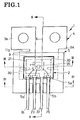
- FIGS. 1-14 of the above drawings are all directed to the first preferred form of current detector according to the invention.
- the representative current detector is broadly divisible as in FIG. 5 into a current-path conductor assembly 1 and a Hall generator assembly 2.
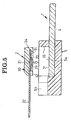
- the two assemblies 1 and 2 are integrally joined together in prescribed positional relationship to each other via an adhesive layer, seen at 3 in both FIGS. 2 and 3, at a final stage of manufacture of this current detector.
- the current-path conductor assembly 1 provides a path for the current to be detected or measured.
- the Hall generator assembly 2 includes a semiconductor chip with a Hall-effect element or Hall generator formed therein for generating a Hall voltage proportional to the magnitude of the current flowing through the current path of the current-path conductor assembly 1.
- the current-path conductor assembly 1 is shown by itself in FIG. 6, and the Hall generator assembly 2 by itself in FIG. 7.
- the current-path conductor assembly 1 comprises a sheet-metal current-path conductor 4, which provides the desired current path through the current detector, and a conductor holder 5 of plastics material molded in one piece with the current-path conductor.
- the current-path conductor 4 is a punching of sheet copper, complete with a nickel plating, that is sufficiently thick to carry current of, say, 100 amperes or so.
- the current-path conductor 4 is generally U-shaped in this particular embodiment as a relatively wide and deep slit 6 is cut therein, providing a pair of limbs 7 and 8 extending in parallel spaced relationship to each other, and a bight 9 joining the limbs each at one end thereof.
- the conductor limbs 7 and 8 are notionally subdivisible, as indicated by the broken lines in FIG. 8, into relatively enlarged distal or terminal portions 7 a and 8 a , and current-path portions 7 b and 8 b through which the terminal portions are joined to the bight 9, another current-path portion.
- the terminal portions 7 a and 8 a of the conductor limbs 7 and 8 have bores 10 a and 10 b formed therein for use in fastening this current detector to a desired electric circuit to be tested.
- the current-path portions 7 b and 8 b of the conductor limbs 7 and 8 are shown to have a pair of slits 11 a and 11 b and another pair of shorter slits 11 c and 11 d , respectively, which are cut inwardly ( i.e. toward the slit 6) from their outer edges. Still another pair of slits 11 e and 11 f are shown formed in the bight 9 of the current-path conductor 4. All these pairs of slits are intended to constrict the current path toward the slit 6 and, in consequence, toward the Hall generator which is to be positioned in register with the slit 6, as will be detailed presently. Besides, in insert-molding the plastic holder 5 with the current-path conductor 4, the slit pairs will help realize firmer engagement of the conductor with the conductor holder, resulting in greater mechanical strength of the current-path conductor assembly 1.
- An additional slit 11 g is shown formed at the boundary between the terminal portion 7 a and current-path portion 7 b of the conductor limb 7. Unlike the other limbs 11 a - 11 f this slit 11 g is intended to make the current-path conductor 4 fusible on carrying a particular value of overload current.
- the conductor holder 5 is designed for mechanically supporting and electrically insulating the current-path conductor 4, as well as, no less importantly, for positioning the Hall generator assembly 2 with respect to the conductor 4 in putting together the current-path conductor assembly 1 and Hall generator assembly 2.
- the conductor holder 5 envelopes part of the current-path conductor 4, leaving exposed all of the pair of terminal portions 7 a and 8 a and parts of the pair of current-path portions 7 b and 8 b and the bight 9. More specifically, as will be seen also from FIGS.
- the conductor holder 5 covers nearly the complete bottom surfaces, as seen in these figures, and parts of the top surfaces, of the pair of current-path portions 7 b and 8 b and the bight 9, and fills part of the slit 6 between the pair of conductor limbs 7 and 8 and all of the slits 11 a -11 f .
- the conductor holder 5 has formed therein recesses or depressions 5 a and 5 b for receiving the Hall generator assembly 2 in prescribed positional relationship to the current-path conductor 4. More will be said presently about these positioning recesses 5 a and 5 b . It will be noted from FIGS. 2, 3 and 5 that the conductor holder 5 is rendered thinner at its portion underlying the current-path conductor 4 than at its portion overlying the same. The thinner portion of the conductor holder 5 is intended for greater heat dissipation. The conductor holder 5 of this shape can be easily formed in one piece with the current-path conductor 4 by the familiar transfer molding method or by injection.
- the Hall generator assembly 2 comprises a semiconductor chip 20 including a Hall generator or Hall-effect device, not shown in this figure, a metal-made mounting plate 21 to which the semiconductor chip is mounted via a layer 91 of magnetic material, a lead 22 of one-piece construction with the mounting plate, three other leads 23, 24 and 25, and a plastic encapsulation 30 enveloping all of the semiconductor chip 20, mounting plate 21, magnetic layer 91, and all but most parts of the leads 22-25.
- the semiconductor chip 20 is of such design (to be detailed later with reference to FIGS. 12-14) that the Hall generator assembly 2 has the four leads 22-25.
- the lead 22 is electrically coupled to the mounting plate 21 and thence to the semiconductor chip by a wire 26 of aluminum or like material, as will be seen also from FIG. 9 which shows the Hall generator assembly minus the encapsulation 30.
- the other leads 23-25 are all connected directly to the semiconductor chip by way of wires 27, 28 and 29, respectively.
- the encapsulation 30 of the Hall generator assembly 2 is generally box-shaped, with a size to fit in the positioning recess 5 a in the conductor holder 5 of the current-path conductor assembly 1. It will also be noted from this figure that the encapsulation 30 includes a bottom surface 32 held against the exposed surface portion 31 of the current-path conductor 4 of the current-path conductor assembly 1, and a side surface 34 to be held against the wall surface 33 defining the positioning recess 5 a .
- the current-path conductor assembly 1 and the Hall generator assembly 2 are bonded together by the adhesive layer 3, FIG.
- the conductor holder 5 and Hall generator encapsulation 30 constitute in combination a unitary casing of the current detector.
- FIG. 4 clearly illustrates that the four Hall generator leads 22-25 are partly received respectively in the positioning recesses 5 b in the conductor holder 5 and thereby held in parallel spaced relationship to one another.
- the conductor holder 5 with the positioning recesses 5 b serves to prevent the leads 22-25 from mutual electrical contact as well as from mechanical deformation or displacement.
- FIGS. 2-4 the Hall generator assembly 2 with the leads 22-25 is received with clearances in the positioning recesses 5 a and 5 b in the conductor holder 5.
- the current-path conductor assembly 1 and Hall generator assembly 2 can be firmly united solely by the adhesive layer 3, it is recommended for still stronger union of the two assemblies 1 and 2 that a suitable adhesive resin be introduced into the clearances therebetween for solidification in situ.
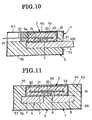
- the resin thus introduced into the clearances is shown at 90 in FIGS. 10 and 11.
- the reference numeral 93 in these figures generally designate the unitary casing for the current detector which is constituted of the current-path conductor holder 5, Hall generator encapsulation 30, adhesive layers 3, and additional resin layers 90.
- the semiconductor chip 20 comprises a Hall-effect device or Hall generator 35, an amplifier 36, and a control current supply circuit 37, which are all conventionally formed in a substrate 42 of semiconductor material (e.g. gallium arsenide or silicon).
- semiconductor material e.g. gallium arsenide or silicon.
- the construction of the semiconductor chip 20 is generally conventional, so that no more detailed illustration of the amplifier 36 and control current supply circuit 37 is considered necessary; only, the Hall generator 35 is shown in further detail in FIGS. 13 and 14 as it bears more or less direct pertinence to the various improvements that are introduced into this current detector by the instant invention.
- the Hall generator 35 is constituted of five n -type semiconductor regions 43, 44, 45, 46 and 47 and three p -type semiconductor regions 48, 49 and 50, which are all formed in the substrate 42 of square shape as seen in a plan view as in FIG. 12.
- the fifth n -type semiconductor region 47 is formed as an island, which is cross-shaped as seen in a plan view as in FIG. 13, in the third p -type semiconductor region 50 which occupies most part of the substrate 42.
- the first and second n -type semiconductor regions 43 and 44 are both formed as islands in the region 47 with a spacing therebetween along the y -axis in FIG. 13.
- Electrodes 51 and 52 are in ohmic contact respectively with the first and second n -type semiconductor regions 43 and 44.
- the electrodes 51 and 52 are both connected to the control current supply circuit 37 in order to cause control current I c to flow through the fifth n -type semiconductor region 47 from the first n -type semiconductor region 43 to the second 44. It is understood that the electrodes 51 and 52 are electrically connected via the control current supply circuit 37 to a pair of terminals 40 and 41, FIG. 12, thereby to be coupled to a direct current power supply, not shown.
- the third and fourth n -type semiconductor regions 45 and 46 are formed adjacent the center of the fifth n -type semiconductor region 47 in the direction of the y -axis and spaced from each other in the direction of the x-axis for detection of the Hall voltage. These regions 45 and 46 are partly contiguous to the fifth n- type semiconductor region 47 and partly to the first and second p -type semiconductor regions 48 and 49. These p -type semiconductor regions 48 and 49 are intended to limit the areas of contact of the third and fourth n -type semiconductor regions 45 and 46 with the fifth n -type semiconductor region 47.
- FIGS. 12 and 14 indicate that electrodes 53 and 54 are in ohmic contact with the third and fourth n -type semiconductor regions 45 and 46. The electrodes 53 and 54 are both electrically coupled to the terminals 38 and 39 via the amplifier 36.
- a Hall voltage will develop between the third and fourth n -type semiconductor regions 45 and 46 in proportion to the strength of the magnetic field applied normal to the flow of the control current I c from the first n -type semiconductor region 43 to the second 44 as in FIG. 11.
- the part of the fifth n -type semiconductor region 47 which lies between the first and second n -type semiconductor regions 43 and 44 and between the third and fourth n -type semiconductor regions 45 and 46 constitutes the "primary working part of the Hall generator 35," a term used in the claims appended hereto, in the narrower sense of the term. Speaking more broadly, however, this term may be construed to refer to the entire fifth n -type semiconductor region 47.
- the semiconductor substrate 42 has an insulating layer 55, as of silicon oxide, formed on one major surface thereof and a metallic layer 56, as of aluminum, on the other major surface thereof.
- the insulating layer 55 takes the form of a lamination of two sublayers 55 a and 55 b for convenience in wiring.
- the electrodes 51 and 52, FIG. 12 are coupled to the first and second n -type semiconductor regions 43 and 44, respectively, via openings in the insulating sublayers 55 a and 55 b.
- the electrodes 53 and 54, FIG. 14, are coupled to the third and fourth n -type semiconductor regions 45 and 46, respectively, via openings in the insulating sublayer 55 a.
- the metallic layer 56 on the other major surface of the substrate 42 is bonded at 57 to the magnetic layer 91, which in turn is bonded at 92 to the mounting plate 21 shown also in FIGS. 1-3 and so forth.
- the bonding agent 57 may be either electrically conductive or insulating.
- the magnetic layer 91 is a layer of magnetic material, preferably a sheet of Permalloy (tradename for a series of highly magnetically permeable iron-base alloys containing approximately 35-80% nickel), with a specific magnetic permeability of 5500 and a thickness of 100 microns.
- An epoxy adhesive is recommended for bonding this magnetic layer 91 to the mounting plate 21.
- the magnetic layer 91 should be larger in area than the Hall generator 35 and, preferably than the actually current-flowing part of the current-path conductor 4.
- the magnetic layer 91 is of the same size as the mounting plate 21 which is substantively larger than the semiconductor chip 20.
- the adhesive layers 57 and 92 shown in FIG. 12 are not in FIGS. 2, 3, 5, 10 and 11 for simplicity.
- the bonding of the magnetic layer 91 to the mounting plate 21 is not a prerequisite, either; in practice, they may be united as by vaporization, deposition or pressurization.
- FIG. 9 best indicates that the mounting plate 21 is generally rectangular in shape, with an area greater than that of the semiconductor chip 20.
- the mounting plate 21 and the four leads 22-25 are punchings made from the same sheet metal material such as sheet copper with a nickel plating, and are less in thickness than the current-path conductor 4.
- the mounting plate 21 is joined directly to the lead 22, which usually is grounded. Additionally, the mounting plate 21 is wired at 26 to the terminal 38, FIG. 12, of the semiconductor chip 20.
- the other terminals 39-41 of the semiconductor chip 20 are wired at 27-29 to the leads 23-25, respectively.
- the mounting plate 21 is laid parallel to the current-path conductor 4.
- the semiconductor chip 20 is so positioned on this mounting plate 21 that, as seen in a plan view as in FIG. 1 or in a direction normal to the parallel planes of the current-path conductor 4 and mounting plate 21, most of the semiconductor chip 20 is in register with the slit 6 between the pair of limbs 7 and 8 of the current-path conductor 4.
- at least the primary working part of the Hall generator 35 is contained in the slit 6 as seen in a plan view.
- the semiconductor substrate 42 is 0.3 millimeter thick in this particular embodiment. There is a spacing of 0.38 millimeter between this semiconductor substrate 42 and the current-path conductor 4.
- the noted unitary casing 93 of this current detector is approximately box-shaped, having a pair of opposite major surfaces 95 and 96 and four side surfaces 97, 98, 99 and 100.
- a layer of magnetic material 94 covers all of the two major surfaces 95 and 96 and two side surfaces 97 and 98, and parts of the other two side surfaces 99 and 100, of the current detector casing 93.
- the magnetic covering 94 leaves parts of the side surfaces 99 and 100 exposed because the Hall generator leads 22-25 and the pair of terminal portions of the current-path conductor 4 project from these surfaces.
- the magnetic covering 94 can also be sheets of Permalloy with a specific magnetic permeability of 5500 and a thickness of 100 microns.
- the Permalloy sheets may be attached to the required surfaces of the current detector casing 93 as by an epoxy adhesive.
- a magnetic layer may be formed on at least part of the major surface 95 of the current detector casing 93 in overlying relationship to the semiconductor chip 20.
- the pair of terminals 7 a and 8 a of the current-path conductor 4 may be connected to the desired electric circuit so that the current to be detected or measured may flow through the U-shaped path of the conductor. Since this current path substantially encircles and closely adjoins the primary working part of the Hall generator 35, as seen in a plan view as in FIG. 1, the current flow through the conductor 4 will produce a magnetic field H , as indicated by the arrows in FIG. 14, effectively acting on the Hall generator. Oriented normal to the direction of the control current I c , FIG.
- the magnetic field H will give rise to the Hall voltage between the pair of n -type semiconductor regions 45 and 46, or between the pair of electrodes 53 and 54.
- This Hall voltage will be in proportion with the strength of the magnetic field H and hence with the magnitude of the current to be detected.
- Test Current Detector No. Sensitivity 1 1.00 2 1.23 3 1.35 4 1.18 5 1.06 6 1.10 7 1.15 8 1.56 9 1.46 10 1.23 11 1.11 12 1.79
- Test Current Detector No. 12 constructed as shown in FIGS. 10 and 11, was the highest in sensitivity, but Test Current Detectors Nos. 2-11 all indicated appreciable improvements in sensitivity. All these Test Current Detectors No. 2-12 are therefore believed to fall within the scope of this invention.
- the current detector shown in these figures is a combination of a current-path conductor assembly 1', FIG. 15, and a Hall generator assembly 2', FIG. 16.
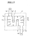
- the current-path conductor assembly 1' comprises a current-path conductor 4 a , shown by itself in FIG. 17, and a conductor holder 5' of plastics material molded in one piece therewith.
- the Hall generator assembly 2' incorporates two Hall-effect elements or Hall generators 35 and 35' of like construction, together with a plastic encapsulation 30' for both Hall generators 35 and 35', and four leads 22', 23', 24' and 25' extending therefrom.
- the current-path conductor 4 a of the current-path conductor assembly 1' is in the shape of a recumbent S, as seen in a plan view as in this figure, for use with the two Hall generators 35 and 35'.
- the current-path conductor 4 a is formed into the shape of an S by cutting two relatively wide slits or elongate openings 6 and 6' from its opposite edges in offset arrangement.
- the two Hall generators 35 and 35', or at least their primary working parts or fifth n -type semiconductor regions 47 and 47', are positioned in register with the slits 6 and 6' as in this figure.
- a plurality of, eight shown by way of example, narrower slits 11 a and 11 b are additionally cut in the current-path conductor 4 a from its outer edges to approximately half the width of the current path for constricting the same toward the Hall generators 35 and 35'.
- the current-path conductor 4 a has an additional slit 11 g .
- This slit 11 g is intended to make the current-path conductor 4 a fusible on carrying a particular value of overload current.
- the current-path conductor 4 a terminates at both ends in a pair of terminal portions 7 a ' and 8 a ' extending in opposite directions therefrom for connection to an electric circuit to be tested.
- the conductor holder 5' is in the shape of a six-sided solid.
- the pair of terminal portion 7 a ' and 7 b ' of the current-path conductor 4 a projects a pair of opposite side surfaces of the conductor holder 5'.
- One major surface of the conductor holder 5' has formed therein a positioning recess 5 a ' for receiving the encapsulation 30' of the Hall generator assembly 2', and a set of elongate positioning recesses 5 b ' for receiving parts of the leads 22'-25' of the Hall generator assembly.
- the two Hall generators 35 and 35' form parts of one and the same semiconductor chip 20' having a semiconductor substrate 42 a , although they could be fabricated as discrete units.
- This semiconductor chip 20' is mounted to the metal-made mounting plate 21 via the magnetic layer 91 which is bonded at 92 to the mounting plate.
- FIG. 19 A comparison of FIG. 19 with FIG. 14 will further reveal that they are each of the same make as the Hall generator 35 of the FIGS. 1-14 embodiment.
- the various parts of the Hall generator 35 are identified by the same reference numerals as used to denote the corresponding parts of the FIG. 14 Hall generator 35, and the various parts of the other Hall generator 35' by priming the reference numerals designating their counterparts of the Hall generator 35.
- the magnetic fields H due to the current flowing through the S -shaped current-path conductor 4 a are opposite in direction for both Hall generators 35 and 35'.
- FIG. 20 shows the electrical circuitry of this current detector.
- the electrodes 51 and 52 of the first Hall generator 35 and the electrodes 51' and 52' of the second Hall generator 35' are all connected to the control current supply circuit 37 a of known design for the flow of the control current I c , FIG. 18, through the Hall generators.
- an output circuit 36 a comprising three differential amplifiers 71, 72 and 73.
- the first differential amplifier 71 has its positive input connected to the third electrode 53 of the first Hall generator 35, and its negative input to the fourth electrode 54 of the first Hall generator.
- the second differential amplifier 72 has its positive input connected to the third electrode 53' of the second Hall generator 35', and its negative input to the fourth electrode 54' of the second Hall generator.
- the Hall voltages V h 1 and -V h 2 produced by the differential amplifiers 71 and 72 are therefore opposite in polarity.
- the third differential amplifier 73 of the output circuit 36 a has its positive input connected to the first differential amplifier 71, and its negative input to the second differential amplifier 72.
- This output from the third differential amplifier 73 could, however, be obtained by substituting an adder therefor and providing an inverter between the second differential amplifier 72 and the adder.
- the current detector of FIGS. 15-20 gains all the advantages accruing from the magnetic layer 91 and magnetic covering 94 which have been set forth in connection with the FIGS. 1-14 embodiment.
- the additional advantages peculiar to this second embodiment are:
- Another modified current-path conductor 4 b of FIG. 21 features a narrow, J-shaped slit 6 a in substitution for the broader, straight slit 6 of the FIGS. 1-14 embodiment.
- This modified current-path conductor 4 b is to be combined with the plastic conductor holder, not shown here, of the same construction as in FIGS. 1-14, and the resulting current-path conductor assembly is to be combined with the Hall-generator assembly, also not shown here, of the same construction as in FIGS. 1-14.
- the current detector including the FIG. 21 current-path conductor 4 c has the Hall generator 35 positioned as indicated by the dashed outline in this figure. It will be noted that the Hall generator 35 is in register with that part 80 of the current-path conductor 4 b which is bounded by the curvature of the J-shaped slit 6 a therein. This part 80, absent from the FIGS. 1-14 current-path conductor 4, functions both as a shield against noise and as a heat dissipater.
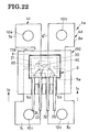
- FIG. 22 a current detector according to the invention as adapted specifically for detection of current leakage.
- the current leakage detector features a modified current-path conductor assembly 1 a which is for use in combination with the Hall generator assembly 2 of the same construction as in FIGS. 1-14.
- the modified current-path conductor assembly 1 a includes a pair of elongate sheet-metal current-path conductors 4 c and 4 d for ease of detection of current leakage.
- a molded plastic conductor holder 150 another component of the current-path conductor assembly 1 b , is formed in one piece with the current-path conductors 4 c and 4 d , holding them parallel to each other with a spacing 6" therebetween which is somewhat functionally equivalent to the slit 6 in the unitary current-path conductor 4 of the FIGS. 1-14 embodiment.
- the Hall generator 35 of the Hall generator assembly 2 is disposed in register with this spacing 6" between the current-path conductors 4 c and 4 d as seen in a plan view as in this figure.
- the pair of current-path conductors 4 c and 4 d terminate in a first pair of terminal portions 7 a and 8 a , each at one end, and in a second pair of such portions 7 c and 8 c each at the other end, either for mutual interconnection or for connection to an external circuit.
- Connection holes 10a and 10 b are cut in the first pair of terminal portions 7 a and 8 a , and similar holes 10 c and 10 d in the second pair of terminal portions 7 c and 8 c .
- the two pairs of terminal portions project in opposite directions from the conductor holder 150.
- the conductor holder 150 has formed therein the positioning recesses 5 a and 5 b for receiving the encapsulation 30 and leads 22-25, respectively, of the Hall generator assembly 2 in prescribed positional relationship to the pair of current-path conductors 4 c and 4 d . It is understood that, so positioned on the conductor holder 150, the Hall generator assembly 2 is bonded to the conductor holder in the same manner as set forth in connection with FIGS. 1-14 embodiment.
- the pair of current-path conductors 4 c and 4 d may be serially connected respectively to the pair of power conductors, not shown, to be tested, in such a way that the currents I a and I b flow in the same direction through the conductors 4 c and 4 d , as indicated by the arrows in FIG. 22.
- the currents I a and I b will be of the same magnitude if there is no leakage.
- the Hall generator 35 will produce no voltage when the currents I a and I b are of the same magnitude, since the magnetic fluxes due to the currents I a and I b act on the Hall generator in opposite directions. In event a current leakage does occur, however, the currents I a and I b will be unequal in magnitude, so that the Hall generator 35 will put out a voltage in proportion with the magnitude of the leaking current.
- FIGS. 22-23 embodiment lends itself to use as a current balance detector as well.
- the Hall voltage proportional to the difference between the magnitudes of two currents I a and I b to be measured will be produced as such currents are made to flow through the pair of current path conductors 4 c and 4 d .
- the FIGS. 22-23 device is readily adaptable for use in the same manner as that of FIGS. 1-14 as the pair of current-path conductors 4 c and 4 d provide the U-shaped current path as its terminal portions 7 c and 8 c , for instance, are electrically interconnected.
- this embodiment incorporates the magnetic layer 91 and magnetic covering 94 as in the FIGS. 1-14 embodiment.
Landscapes
- Physics & Mathematics (AREA)
- General Physics & Mathematics (AREA)
- Measuring Instrument Details And Bridges, And Automatic Balancing Devices (AREA)
- Hall/Mr Elements (AREA)
- Measuring Magnetic Variables (AREA)
- Transformers For Measuring Instruments (AREA)
Abstract
Description
or
| Test Current Detector No. | |
| 1 | 1.00 |
| 2 | 1.23 |
| 3 | 1.35 |
| 4 | 1.18 |
| 5 | 1.06 |
| 6 | 1.10 |
| 7 | 1.15 |
| 8 | 1.56 |
| 9 | 1.46 |
| 10 | 1.23 |
| 11 | 1.11 |
| 12 | 1.79 |
Claims (21)
- A current detector utilizing the Hall-effect for detection or measurement of electric current, comprising a current-path conductor (4) for carrying current to be detected or measured, and a Hall generator (35) disposed opposite the current-path conductor for generating a Hall voltage proportional to the strength of a magnetic field due to the current flowing through the current-path conductor, characterized in that a magnetic layer means (91 or 94) is disposed opposite the current-path conductor (4 or 4 a or 4 b or 4 c ) via the Hall generator (35), and that a casing (93 consisting of 5 or 5' or 150 and 30) of electrically insulating material holds the current-path conductor and the Hall generator and the magnetic layer means in prescribed relative positions.
- A current detector as claimed in claim 1, characterized in that the casing (93) envelopes the Hall generator (35) and part of the current-path conductor (4 or 4 a or 4 b or 4 c ), and that the magnetic layer means is a magnetic layer (91) enveloped by the casing.
- A current detector as claimed in claim 2, characterized in that the Hall generator (35) is mounted via the magnetic layer (91) to a metal-made mounting plate (21) which is enveloped by the casing (93).
- A current detector as claimed in claim 1, characterized in that the casing (93) envelopes the Hall generator (35) and part of the current-path conductor (4 or 4 a or 4 b or 4 c ), and that the magnetic layer means is a magnetic covering (94). which covers at least part of the casing (93).
- A current detector as claimed in claim 1, characterized in that the casing (93) envelopes the Hall generator (35) and part of the current-path conductor (4 or 4 a or 4 b or 4 c ), and that the magnetic layer means comprises a magnetic layer (91) enveloped by the casing, and a magnetic covering (94) which covers at least part of the casing.
- A current detector as claimed in claim 1, characterized in that the current-path conductor (4 or 4 a or 4 b or 4 c ) has a slit (11 a or 11 g ) formed therein to constrict the current path.
- A current detector utilizing the Hall-effect for detection or measurement of electric current, characterized in that the current detector is a combination of a current-path conductor assembly (1 or 1' or 1 a ) and a Hall generator assembly (2), and that the current-path conductor assembly comprises a current-path conductor (4 or 4 a or 4 b or 4 c ) in the form of a piece of sheet metal for carrying current to be detected or measured and a conductor holder (5 or 5' or 150) of electrically insulating material integrally holding the current-path conductor, and that the Hall generator assembly (2) comprises a Hall generator (35) for generating a Hall voltage proportional to the strength of an applied magnetic field, a magnetic layer (91) held against the Hall generator and an encapsulation (30) of electrically insulating material integrally enveloping the Hall generator and the magnetic layer, and that the current-path conductor assembly (1 or 1' or 1 a ) and the Hall generator assembly (2) are combined by bonding together the conductor holder (5 or 5' or 150) of the current-path conductor assembly and the encapsulation (30) of the Hall generator assembly into a unitary casing (93) for the current detector, with the Hall generator (35) positioned adjacent the current-path conductor (4 or 4 a or 4 b or 4 c ) for generating the Hall voltage in response to a magnetic field due to the current flowing through the current-path conductor.
- A current detector as claimed in claim 7, characterized in that the casing (93) is at least partly enveloped by a covering (94) of magnetic material.
- A current detector as claimed in claim 7, characterized in that the current-path conductor is a piece of sheet metal having a slit (6 or 6 a ) formed therein to provide a U-shaped current path around the Hall generator (35), and that the Hall generator (35) has a primary working part contained in the slit (6 or 6 a ) in the current-path conductor as seen in a direction normal to the plane of the sheet-metal current-path conductor.
- A current detector as claimed in claim 9, characterized in that the current-path conductor has a slit (11 a or 11 g ) formed therein to constrict the current path.
- A current detector utilizing the Hall-effect for detection or measurement of electric current, characterized in that the current detector is a combination of a current-path conductor (4 a ) in the form of a piece of sheet metal adapted to provide an S-shaped current path for carrying current to be detected or measured, Hall generator means comprising a pair of Hall generators (35, 35') disposed opposite the current-path conductor in positions spaced along the S-shaped current path each for generating a Hall voltage proportional to the strength of a magnetic field due to the current flowing through the current-path conductor, an output circuit (36 a ) for combining the Hall voltages generated by the Hall generators, magnetic layer means disposed opposite current-path conductor via the Hall generator means, and a casing (5', 30') of electrically insulating material holding the current-path conductor and the Hall generator means in prescribed relative positions.
- A current detector as claimed in claim 11, characterized in that the casing envelopes the Hall generator means (35, 35') and part of the current-path conductor (4 a ), and that the magnetic layer means comprises a magnetic layer (91) enveloped by the casing.
- A current detector as claimed in claim 12, characterized in that the Hall generator means (35, 35') is mounted via the magnetic layer (91) to a metal-made mounting plate (21), and that the metal-made mounting plate (21) is enveloped by the casing.
- A current detector as claimed in claim 11, characterized in that the casing envelopes the Hall generator means (35, 35') and part of the current-path conductor (4 a ), and that the magnetic layer means comprises a magnetic covering (94) which covers at least part of the casing.
- A current detector as claimed in claim 11, characterized in that the casing envelopes the Hall generator means (35, 35') and part of the current-path conductor (4 a ), and that the magnetic layer means comprises a magnetic layer (91) enveloped by the casing, and a magnetic covering (94) which covers at least part of the casing.
- A current detector as claimed in claim 11, characterized in that the current-path conductor has a slit (11 a or 11 g ) formed therein to constrict the current path.
- A current detector utilizing the Hall-effect for detection or measurement of electric current, characterized in that the current detector is a combination of a pair of elongate current-path conductors (4 c , 4 d ) each for carrying current to be detected or measured, the pair of current-path conductors extending in parallel spaced relationship to each other and each terminating in a pair of terminal portions (7 a , 7 c ; 8 a , 8 c ) at both ends thereof, a Hall generator (35) disposed opposite the pair of current-path conductors for generating a Hall voltage proportional to a difference between the magnitudes of currents flowing through the respective current-path conductors, magnetic layer means (91 or 94 or 91 and 94) disposed opposite the pair of current-path conductors via the Hall generator, and a casing (30, 150) of electrically insulating material holing the pair of current-path conductors and the Hall generator in prescribed relative positions.
- A current detector as claimed in claim 17, characterized in that the casing envelopes (30, 150) the Hall generator (35) and parts of the pair of current-path conductors (4 c , 4 d ), and that the magnetic layer means comprises a magnetic layer enveloped by the casing.
- A current detector as claimed in claim 18, characterized in that the Hall generator (35) is mounted via the magnetic layer to a metal-made mounting plate (21) ,and that the metal-made mounting plate (21) is enveloped by the casing.
- A current detector as claimed in claim 17, characterized in that the casing envelopes the Hall generator (35) and parts of the pair of current-path conductors (4 c , 4 d ), and that the magnetic layer means comprises a magnetic covering which covers at least part of the casing.
- A current detector as claimed in claim 17, characterized in that the casing envelopes the Hall generator (35) and parts of the pair of current-path conductors (4 c , 4 d ), and that the magnetic layer means comprises a magnetic layer enveloped by the casing, and a magnetic covering which covers at least part of the casing.
Applications Claiming Priority (2)
| Application Number | Priority Date | Filing Date | Title |
|---|---|---|---|
| JP2001182287 | 2001-06-15 | ||
| JP2001182287A JP4164626B2 (en) | 2001-06-15 | 2001-06-15 | CURRENT DETECTOR HAVING HALL ELEMENT |
Publications (2)
| Publication Number | Publication Date |
|---|---|
| EP1271159A2 true EP1271159A2 (en) | 2003-01-02 |
| EP1271159A3 EP1271159A3 (en) | 2005-04-20 |
Family
ID=19022425
Family Applications (1)
| Application Number | Title | Priority Date | Filing Date |
|---|---|---|---|
| EP02012389A Withdrawn EP1271159A3 (en) | 2001-06-15 | 2002-06-06 | Hall-effect current detector |
Country Status (3)
| Country | Link |
|---|---|
| US (1) | US6759841B2 (en) |
| EP (1) | EP1271159A3 (en) |
| JP (1) | JP4164626B2 (en) |
Cited By (5)
| Publication number | Priority date | Publication date | Assignee | Title |
|---|---|---|---|---|
| DE10323379A1 (en) * | 2003-05-23 | 2004-06-24 | Infineon Technologies Ag | Integrated circuit has Hall probe structure arranged close to conducting track so Hall voltage dependent on measurement voltage can be measured depending on magnetic field caused by track current |
| DE102004054317A1 (en) * | 2004-11-10 | 2006-05-11 | Mitsubishi Denki K.K. | Current measurer has measuring circuit for a current channel on a substrate with a magnetic flux measurer and slots to concentrate the flux |
| EP1882953A1 (en) * | 2006-07-26 | 2008-01-30 | Siemens Aktiengesellschaft | Current measuring device |
| EP2894489A1 (en) * | 2014-01-13 | 2015-07-15 | Micronas GmbH | Sensor device |
| CN111370572A (en) * | 2020-02-28 | 2020-07-03 | 浙江长兴电子厂有限公司 | A kind of hermetic current sensor inverted welding package structure |
Families Citing this family (60)
| Publication number | Priority date | Publication date | Assignee | Title |
|---|---|---|---|---|
| US6853178B2 (en) * | 2000-06-19 | 2005-02-08 | Texas Instruments Incorporated | Integrated circuit leadframes patterned for measuring the accurate amplitude of changing currents |
| US7259545B2 (en) * | 2003-02-11 | 2007-08-21 | Allegro Microsystems, Inc. | Integrated sensor |
| EP1450176A1 (en) * | 2003-02-21 | 2004-08-25 | Liaisons Electroniques-Mecaniques Lem S.A. | Magnetic field sensor and electrical current sensor therewith |
| US7709754B2 (en) * | 2003-08-26 | 2010-05-04 | Allegro Microsystems, Inc. | Current sensor |
| US7476816B2 (en) * | 2003-08-26 | 2009-01-13 | Allegro Microsystems, Inc. | Current sensor |
| US20060219436A1 (en) * | 2003-08-26 | 2006-10-05 | Taylor William P | Current sensor |
| EP1781820B1 (en) * | 2004-08-20 | 2018-04-04 | Magnomics, SA | A bio-electronic device |
| US7777607B2 (en) * | 2004-10-12 | 2010-08-17 | Allegro Microsystems, Inc. | Resistor having a predetermined temperature coefficient |
| KR20080036618A (en) | 2005-09-05 | 2008-04-28 | 스미토모 베이클라이트 가부시키가이샤 | Cutting winding device and cutting winding method of tubular resin film |
| EP1772737A3 (en) * | 2005-10-08 | 2008-02-20 | Melexis Technologies SA | Assembly group for the current measurement |
| JP2007121239A (en) * | 2005-10-31 | 2007-05-17 | Denso Corp | Current sensor and manufacturing method thereof |
| US7768083B2 (en) | 2006-01-20 | 2010-08-03 | Allegro Microsystems, Inc. | Arrangements for an integrated sensor |
| US20070279053A1 (en) * | 2006-05-12 | 2007-12-06 | Taylor William P | Integrated current sensor |
| JP2009052898A (en) * | 2007-08-23 | 2009-03-12 | Mitsubishi Electric Corp | Current detection board |
| US7795862B2 (en) | 2007-10-22 | 2010-09-14 | Allegro Microsystems, Inc. | Matching of GMR sensors in a bridge |
| US7816905B2 (en) | 2008-06-02 | 2010-10-19 | Allegro Microsystems, Inc. | Arrangements for a current sensing circuit and integrated current sensor |
| US8093670B2 (en) * | 2008-07-24 | 2012-01-10 | Allegro Microsystems, Inc. | Methods and apparatus for integrated circuit having on chip capacitor with eddy current reductions |
| US7973527B2 (en) | 2008-07-31 | 2011-07-05 | Allegro Microsystems, Inc. | Electronic circuit configured to reset a magnetoresistance element |
| US8063634B2 (en) * | 2008-07-31 | 2011-11-22 | Allegro Microsystems, Inc. | Electronic circuit and method for resetting a magnetoresistance element |
| US8400139B2 (en) * | 2010-03-26 | 2013-03-19 | Infineon Technologies Ag | Sensor package having a sensor chip |
| US9013890B2 (en) | 2010-03-26 | 2015-04-21 | Infineon Technologies Ag | Semiconductor packages and methods for producing the same |
| US8994370B2 (en) * | 2010-07-30 | 2015-03-31 | Peugeot Citroën Automobiles SA | Magnetoresistor integrated sensor for measuring voltage or current, and diagnostic system |
| JP5809793B2 (en) * | 2010-11-17 | 2015-11-11 | 矢崎総業株式会社 | Battery terminal with current sensor |
| EP2641298B1 (en) | 2010-11-17 | 2020-03-04 | Yazaki Corporation | Battery terminal with current sensor |
| JP5938778B2 (en) * | 2010-11-17 | 2016-06-22 | 矢崎総業株式会社 | Battery terminal with current sensor |
| JP5730072B2 (en) * | 2011-02-25 | 2015-06-03 | 富士通コンポーネント株式会社 | Current sensor, table tap with current sensor, current sensor cover |
| US8969985B2 (en) * | 2011-08-30 | 2015-03-03 | Infineon Technologies Ag | Semiconductor chip package and method |
| US8629539B2 (en) | 2012-01-16 | 2014-01-14 | Allegro Microsystems, Llc | Methods and apparatus for magnetic sensor having non-conductive die paddle |
| US9666788B2 (en) | 2012-03-20 | 2017-05-30 | Allegro Microsystems, Llc | Integrated circuit package having a split lead frame |
| US9812588B2 (en) | 2012-03-20 | 2017-11-07 | Allegro Microsystems, Llc | Magnetic field sensor integrated circuit with integral ferromagnetic material |
| US10234513B2 (en) | 2012-03-20 | 2019-03-19 | Allegro Microsystems, Llc | Magnetic field sensor integrated circuit with integral ferromagnetic material |
| US9494660B2 (en) | 2012-03-20 | 2016-11-15 | Allegro Microsystems, Llc | Integrated circuit package having a split lead frame |
| JP5866596B2 (en) * | 2012-11-14 | 2016-02-17 | アルプス・グリーンデバイス株式会社 | Current sensor |
| US9190606B2 (en) | 2013-03-15 | 2015-11-17 | Allegro Micosystems, LLC | Packaging for an electronic device |
| US10345343B2 (en) | 2013-03-15 | 2019-07-09 | Allegro Microsystems, Llc | Current sensor isolation |
| US9411025B2 (en) | 2013-04-26 | 2016-08-09 | Allegro Microsystems, Llc | Integrated circuit package having a split lead frame and a magnet |
| US9354284B2 (en) | 2014-05-07 | 2016-05-31 | Allegro Microsystems, Llc | Magnetic field sensor configured to measure a magnetic field in a closed loop manner |
| US9322887B1 (en) | 2014-12-01 | 2016-04-26 | Allegro Microsystems, Llc | Magnetic field sensor with magnetoresistance elements and conductive-trace magnetic source |
| CN105116214A (en) * | 2015-08-31 | 2015-12-02 | 重庆京东方光电科技有限公司 | Power detection device |
| JP2017134022A (en) * | 2016-01-29 | 2017-08-03 | 旭化成エレクトロニクス株式会社 | Electric current sensor and manufacturing method |
| WO2018051575A1 (en) * | 2016-09-14 | 2018-03-22 | 旭化成エレクトロニクス株式会社 | Electric current sensor |
| CN107390003B (en) * | 2017-08-21 | 2023-09-01 | 浙江中凯科技股份有限公司 | Hall current detection device |
| US10935612B2 (en) | 2018-08-20 | 2021-03-02 | Allegro Microsystems, Llc | Current sensor having multiple sensitivity ranges |
| US11029373B2 (en) * | 2019-07-16 | 2021-06-08 | Allegro Microsystems, Llc | Magnetic field sensors having a magnetic anti-aliasing filter |
| US10991644B2 (en) | 2019-08-22 | 2021-04-27 | Allegro Microsystems, Llc | Integrated circuit package having a low profile |
| US11187764B2 (en) | 2020-03-20 | 2021-11-30 | Allegro Microsystems, Llc | Layout of magnetoresistance element |
| US11800813B2 (en) | 2020-05-29 | 2023-10-24 | Allegro Microsystems, Llc | High isolation current sensor |
| EP3974845B1 (en) * | 2020-09-24 | 2025-12-03 | Melexis Technologies SA | Current sensor system |
| US11320466B1 (en) | 2020-10-29 | 2022-05-03 | Allegro Microsystems, Llc | Differential current sensor |
| CN113658783A (en) * | 2020-11-19 | 2021-11-16 | 四川泰克电器有限公司 | Medium-voltage low-frequency mutual inductor |
| US11402409B1 (en) | 2021-03-22 | 2022-08-02 | Allegro Microsystems, Llc | Differential current sensor package |
| US11567108B2 (en) | 2021-03-31 | 2023-01-31 | Allegro Microsystems, Llc | Multi-gain channels for multi-range sensor |
| EP4130772B1 (en) | 2021-08-05 | 2025-07-23 | Allegro MicroSystems, LLC | Magnetoresistive element having compensated temperature coefficient of tmr |
| JP7614992B2 (en) * | 2021-09-16 | 2025-01-16 | 株式会社東芝 | Current Detector |
| EP4407324A4 (en) * | 2022-01-14 | 2025-01-08 | Aisin Corporation | ELECTRICAL CURRENT SENSOR DEVICE |
| US11768230B1 (en) | 2022-03-30 | 2023-09-26 | Allegro Microsystems, Llc | Current sensor integrated circuit with a dual gauge lead frame |
| DE102022207854A1 (en) | 2022-07-29 | 2024-02-01 | Continental Automotive Technologies GmbH | Current sensor |
| DE102022207853A1 (en) * | 2022-07-29 | 2024-02-01 | Continental Automotive Technologies GmbH | Current sensor |
| US12248039B2 (en) | 2023-08-08 | 2025-03-11 | Allegro Microsystems, Llc | Interleaving sub-arrays of magnetoresistance elements based on reference directions to compensate for bridge offset |
| US12510611B2 (en) | 2023-11-07 | 2025-12-30 | Allegro Microsystems, Llc | TMR sensor having magnetic field generation for pillar stimulation |
Family Cites Families (14)
| Publication number | Priority date | Publication date | Assignee | Title |
|---|---|---|---|---|
| US3845445A (en) * | 1973-11-12 | 1974-10-29 | Ibm | Modular hall effect device |
| US4283643A (en) * | 1979-05-25 | 1981-08-11 | Electric Power Research Institute, Inc. | Hall sensing apparatus |
| US4539520A (en) * | 1981-03-02 | 1985-09-03 | Bridges Electric, Inc. | Remote current detector |
| US5041780A (en) * | 1988-09-13 | 1991-08-20 | California Institute Of Technology | Integrable current sensors |
| JPH07280845A (en) * | 1994-04-14 | 1995-10-27 | Yazaki Corp | Current detector |
| EP0772046B1 (en) * | 1995-10-30 | 2002-04-17 | Sentron Ag | Magnetic field probe and current or energy probe |
| DE69834043T2 (en) * | 1997-09-15 | 2006-11-16 | Ams International Ag | A POWER MONITORING DEVICE AND A METHOD OF MANUFACTURING THEM |
| JP3464369B2 (en) * | 1997-10-17 | 2003-11-10 | 旭化成電子株式会社 | Method of manufacturing thin high-sensitivity Hall element |
| JP2000174357A (en) | 1998-10-02 | 2000-06-23 | Sanken Electric Co Ltd | Semiconductor device having a ball effect element |
| EP1031844A3 (en) * | 1999-02-25 | 2009-03-11 | Liaisons Electroniques-Mecaniques Lem S.A. | Process for forming an electrical current sensor |
| JP2000321309A (en) * | 1999-05-11 | 2000-11-24 | Yazaki Corp | Fixed type current detector |
| JP3681584B2 (en) * | 1999-08-27 | 2005-08-10 | 矢崎総業株式会社 | Current sensor and electric circuit using the same |
| DE19946935B4 (en) * | 1999-09-30 | 2004-02-05 | Daimlerchrysler Ag | Device for inductive current measurement with at least one differential sensor |
| JP3852554B2 (en) * | 1999-12-09 | 2006-11-29 | サンケン電気株式会社 | Current detection device with Hall element |
-
2001
- 2001-06-15 JP JP2001182287A patent/JP4164626B2/en not_active Expired - Fee Related
-
2002
- 2002-06-06 EP EP02012389A patent/EP1271159A3/en not_active Withdrawn
- 2002-06-14 US US10/172,200 patent/US6759841B2/en not_active Expired - Lifetime
Cited By (8)
| Publication number | Priority date | Publication date | Assignee | Title |
|---|---|---|---|---|
| DE10323379A1 (en) * | 2003-05-23 | 2004-06-24 | Infineon Technologies Ag | Integrated circuit has Hall probe structure arranged close to conducting track so Hall voltage dependent on measurement voltage can be measured depending on magnetic field caused by track current |
| DE102004054317A1 (en) * | 2004-11-10 | 2006-05-11 | Mitsubishi Denki K.K. | Current measurer has measuring circuit for a current channel on a substrate with a magnetic flux measurer and slots to concentrate the flux |
| DE102004054317B4 (en) * | 2004-11-10 | 2014-05-15 | Mitsubishi Denki K.K. | Current measuring device |
| EP1882953A1 (en) * | 2006-07-26 | 2008-01-30 | Siemens Aktiengesellschaft | Current measuring device |
| EP2894489A1 (en) * | 2014-01-13 | 2015-07-15 | Micronas GmbH | Sensor device |
| US9632148B2 (en) | 2014-01-13 | 2017-04-25 | Micronas Gmbh | Sensor device |
| CN111370572A (en) * | 2020-02-28 | 2020-07-03 | 浙江长兴电子厂有限公司 | A kind of hermetic current sensor inverted welding package structure |
| CN111370572B (en) * | 2020-02-28 | 2023-11-10 | 浙江东瓷科技有限公司 | Reverse buckling welding packaging structure of airtight current sensor |
Also Published As
| Publication number | Publication date |
|---|---|
| US6759841B2 (en) | 2004-07-06 |
| EP1271159A3 (en) | 2005-04-20 |
| JP4164626B2 (en) | 2008-10-15 |
| JP2003004774A (en) | 2003-01-08 |
| US20030001559A1 (en) | 2003-01-02 |
Similar Documents
| Publication | Publication Date | Title |
|---|---|---|
| US6759841B2 (en) | Hall-effect current detector | |
| US6841989B2 (en) | Hall-effect current detector | |
| EP1281974B1 (en) | Hall-effect current detector | |
| US6545457B2 (en) | Current detector utilizing hall effect | |
| US6791313B2 (en) | Electrical current detector having a U-shaped current path and hall-effect device | |
| US6462531B1 (en) | Current detector having a hall-effect device | |
| US6812687B1 (en) | Semiconductor current detector of improved noise immunity | |
| US6424018B1 (en) | Semiconductor device having a hall-effect element | |
| US6781358B2 (en) | Hall-effect current detector | |
| JP4164629B2 (en) | Current detection device with Hall element | |
| US6769166B1 (en) | Method of making an electrical current sensor | |
| JP2001339109A (en) | Current detection device equipped with a ball element | |
| AU603382B2 (en) | Measuring transformers | |
| JP4025958B2 (en) | CURRENT DETECTOR HAVING HALL ELEMENT | |
| JP3230580B2 (en) | Current detection device equipped with a ball element | |
| JP2002202327A (en) | Current detector equipped with hall element | |
| JP4200358B2 (en) | Current detection device with Hall element | |
| WO2021039264A1 (en) | Electrical current sensor | |
| JP4164625B2 (en) | CURRENT DETECTOR HAVING HALL ELEMENT | |
| JP4164624B2 (en) | CURRENT DETECTOR HAVING HALL ELEMENT | |
| WO2022030140A1 (en) | Current sensor |
Legal Events
| Date | Code | Title | Description |
|---|---|---|---|
| PUAI | Public reference made under article 153(3) epc to a published international application that has entered the european phase |
Free format text: ORIGINAL CODE: 0009012 |
|
| AK | Designated contracting states |
Kind code of ref document: A2 Designated state(s): AT BE CH CY DE DK ES FI FR GB GR IE IT LI LU MC NL PT SE TR |
|
| AX | Request for extension of the european patent |
Free format text: AL;LT;LV;MK;RO;SI |
|
| PUAL | Search report despatched |
Free format text: ORIGINAL CODE: 0009013 |
|
| AK | Designated contracting states |
Kind code of ref document: A3 Designated state(s): AT BE CH CY DE DK ES FI FR GB GR IE IT LI LU MC NL PT SE TR |
|
| AX | Request for extension of the european patent |
Extension state: AL LT LV MK RO SI |
|
| 17P | Request for examination filed |
Effective date: 20050818 |
|
| AKX | Designation fees paid |
Designated state(s): DE FR NL |
|
| STAA | Information on the status of an ep patent application or granted ep patent |
Free format text: STATUS: THE APPLICATION HAS BEEN WITHDRAWN |
|
| 18W | Application withdrawn |
Effective date: 20060504 |