EP1267420B1 - Light emitting diodes with improved light extraction efficiency - Google Patents
Light emitting diodes with improved light extraction efficiency Download PDFInfo
- Publication number
- EP1267420B1 EP1267420B1 EP01204002.8A EP01204002A EP1267420B1 EP 1267420 B1 EP1267420 B1 EP 1267420B1 EP 01204002 A EP01204002 A EP 01204002A EP 1267420 B1 EP1267420 B1 EP 1267420B1
- Authority
- EP
- European Patent Office
- Prior art keywords
- optical element
- light emitting
- emitting device
- bonding layer
- led die
- Prior art date
- Legal status (The legal status is an assumption and is not a legal conclusion. Google has not performed a legal analysis and makes no representation as to the accuracy of the status listed.)
- Expired - Lifetime
Links
- 238000000605 extraction Methods 0.000 title description 14
- 230000003287 optical effect Effects 0.000 claims description 165
- 239000000463 material Substances 0.000 claims description 62
- 239000004065 semiconductor Substances 0.000 claims description 51
- 238000001465 metallisation Methods 0.000 claims description 20
- 239000005304 optical glass Substances 0.000 claims description 12
- 150000001875 compounds Chemical class 0.000 claims description 9
- 229910052594 sapphire Inorganic materials 0.000 claims description 8
- 239000010980 sapphire Substances 0.000 claims description 8
- JNDMLEXHDPKVFC-UHFFFAOYSA-N aluminum;oxygen(2-);yttrium(3+) Chemical compound [O-2].[O-2].[O-2].[Al+3].[Y+3] JNDMLEXHDPKVFC-UHFFFAOYSA-N 0.000 claims description 6
- 229910003460 diamond Inorganic materials 0.000 claims description 6
- 239000010432 diamond Substances 0.000 claims description 6
- 229910019901 yttrium aluminum garnet Inorganic materials 0.000 claims description 6
- 229910001512 metal fluoride Inorganic materials 0.000 claims description 5
- 239000003989 dielectric material Substances 0.000 claims description 4
- -1 nitride compounds Chemical class 0.000 claims description 4
- WATWJIUSRGPENY-UHFFFAOYSA-N antimony atom Chemical class [Sb] WATWJIUSRGPENY-UHFFFAOYSA-N 0.000 claims description 3
- 229910044991 metal oxide Inorganic materials 0.000 claims description 3
- 150000004706 metal oxides Chemical class 0.000 claims description 3
- 229910005540 GaP Inorganic materials 0.000 claims description 2
- RVTZCBVAJQQJTK-UHFFFAOYSA-N oxygen(2-);zirconium(4+) Chemical compound [O-2].[O-2].[Zr+4] RVTZCBVAJQQJTK-UHFFFAOYSA-N 0.000 claims description 2
- 229910001928 zirconium oxide Inorganic materials 0.000 claims description 2
- 229910003465 moissanite Inorganic materials 0.000 claims 1
- 229910010271 silicon carbide Inorganic materials 0.000 claims 1
- 229910052950 sphalerite Inorganic materials 0.000 claims 1
- 229910052984 zinc sulfide Inorganic materials 0.000 claims 1
- 239000004593 Epoxy Substances 0.000 description 38
- 239000008393 encapsulating agent Substances 0.000 description 22
- 238000000034 method Methods 0.000 description 20
- 238000010586 diagram Methods 0.000 description 14
- 239000002245 particle Substances 0.000 description 10
- OAICVXFJPJFONN-UHFFFAOYSA-N Phosphorus Chemical compound [P] OAICVXFJPJFONN-UHFFFAOYSA-N 0.000 description 9
- 230000008569 process Effects 0.000 description 9
- 239000011521 glass Substances 0.000 description 7
- 239000000758 substrate Substances 0.000 description 7
- 238000010521 absorption reaction Methods 0.000 description 5
- 238000005530 etching Methods 0.000 description 5
- 230000001965 increasing effect Effects 0.000 description 5
- 229910052751 metal Inorganic materials 0.000 description 5
- 239000002184 metal Substances 0.000 description 5
- 230000009102 absorption Effects 0.000 description 4
- 239000005387 chalcogenide glass Substances 0.000 description 4
- 239000011248 coating agent Substances 0.000 description 4
- 238000000576 coating method Methods 0.000 description 4
- 239000000956 alloy Substances 0.000 description 3
- 229910045601 alloy Inorganic materials 0.000 description 3
- 238000005229 chemical vapour deposition Methods 0.000 description 3
- 230000007547 defect Effects 0.000 description 3
- 238000000151 deposition Methods 0.000 description 3
- 230000000694 effects Effects 0.000 description 3
- AMGQUBHHOARCQH-UHFFFAOYSA-N indium;oxotin Chemical compound [In].[Sn]=O AMGQUBHHOARCQH-UHFFFAOYSA-N 0.000 description 3
- 238000010884 ion-beam technique Methods 0.000 description 3
- 238000004943 liquid phase epitaxy Methods 0.000 description 3
- 238000003801 milling Methods 0.000 description 3
- 239000000203 mixture Substances 0.000 description 3
- 238000001020 plasma etching Methods 0.000 description 3
- 238000000927 vapour-phase epitaxy Methods 0.000 description 3
- 229910004613 CdTe Inorganic materials 0.000 description 2
- 229910001218 Gallium arsenide Inorganic materials 0.000 description 2
- PXHVJJICTQNCMI-UHFFFAOYSA-N Nickel Chemical compound [Ni] PXHVJJICTQNCMI-UHFFFAOYSA-N 0.000 description 2
- KDLHZDBZIXYQEI-UHFFFAOYSA-N Palladium Chemical compound [Pd] KDLHZDBZIXYQEI-UHFFFAOYSA-N 0.000 description 2
- BQCADISMDOOEFD-UHFFFAOYSA-N Silver Chemical compound [Ag] BQCADISMDOOEFD-UHFFFAOYSA-N 0.000 description 2
- 238000005275 alloying Methods 0.000 description 2
- 238000004458 analytical method Methods 0.000 description 2
- 230000005540 biological transmission Effects 0.000 description 2
- UHYPYGJEEGLRJD-UHFFFAOYSA-N cadmium(2+);selenium(2-) Chemical compound [Se-2].[Cd+2] UHYPYGJEEGLRJD-UHFFFAOYSA-N 0.000 description 2
- 238000009833 condensation Methods 0.000 description 2
- 239000004020 conductor Substances 0.000 description 2
- 238000001816 cooling Methods 0.000 description 2
- 230000003247 decreasing effect Effects 0.000 description 2
- 230000008021 deposition Effects 0.000 description 2
- 238000009792 diffusion process Methods 0.000 description 2
- 239000000975 dye Substances 0.000 description 2
- 125000003700 epoxy group Chemical group 0.000 description 2
- 230000008020 evaporation Effects 0.000 description 2
- 238000001704 evaporation Methods 0.000 description 2
- 230000009477 glass transition Effects 0.000 description 2
- 238000010438 heat treatment Methods 0.000 description 2
- 230000008018 melting Effects 0.000 description 2
- 238000002844 melting Methods 0.000 description 2
- 150000002739 metals Chemical class 0.000 description 2
- 238000001451 molecular beam epitaxy Methods 0.000 description 2
- 239000002159 nanocrystal Substances 0.000 description 2
- BASFCYQUMIYNBI-UHFFFAOYSA-N platinum Chemical compound [Pt] BASFCYQUMIYNBI-UHFFFAOYSA-N 0.000 description 2
- 229920000647 polyepoxide Polymers 0.000 description 2
- 229920000642 polymer Polymers 0.000 description 2
- 229920001296 polysiloxane Polymers 0.000 description 2
- 239000002096 quantum dot Substances 0.000 description 2
- SBIBMFFZSBJNJF-UHFFFAOYSA-N selenium;zinc Chemical compound [Se]=[Zn] SBIBMFFZSBJNJF-UHFFFAOYSA-N 0.000 description 2
- 229910052709 silver Inorganic materials 0.000 description 2
- 239000004332 silver Substances 0.000 description 2
- 238000007711 solidification Methods 0.000 description 2
- 230000008023 solidification Effects 0.000 description 2
- 238000004544 sputter deposition Methods 0.000 description 2
- 235000012431 wafers Nutrition 0.000 description 2
- 229910017115 AlSb Inorganic materials 0.000 description 1
- VYZAMTAEIAYCRO-UHFFFAOYSA-N Chromium Chemical compound [Cr] VYZAMTAEIAYCRO-UHFFFAOYSA-N 0.000 description 1
- 229910002601 GaN Inorganic materials 0.000 description 1
- 229910005542 GaSb Inorganic materials 0.000 description 1
- 229910000673 Indium arsenide Inorganic materials 0.000 description 1
- GPXJNWSHGFTCBW-UHFFFAOYSA-N Indium phosphide Chemical compound [In]#P GPXJNWSHGFTCBW-UHFFFAOYSA-N 0.000 description 1
- KJTLSVCANCCWHF-UHFFFAOYSA-N Ruthenium Chemical compound [Ru] KJTLSVCANCCWHF-UHFFFAOYSA-N 0.000 description 1
- GWEVSGVZZGPLCZ-UHFFFAOYSA-N Titan oxide Chemical compound O=[Ti]=O GWEVSGVZZGPLCZ-UHFFFAOYSA-N 0.000 description 1
- RTAQQCXQSZGOHL-UHFFFAOYSA-N Titanium Chemical compound [Ti] RTAQQCXQSZGOHL-UHFFFAOYSA-N 0.000 description 1
- WGLPBDUCMAPZCE-UHFFFAOYSA-N Trioxochromium Chemical compound O=[Cr](=O)=O WGLPBDUCMAPZCE-UHFFFAOYSA-N 0.000 description 1
- 238000001015 X-ray lithography Methods 0.000 description 1
- 229910007709 ZnTe Inorganic materials 0.000 description 1
- 239000000853 adhesive Substances 0.000 description 1
- 230000001070 adhesive effect Effects 0.000 description 1
- 229910052782 aluminium Inorganic materials 0.000 description 1
- XAGFODPZIPBFFR-UHFFFAOYSA-N aluminium Chemical compound [Al] XAGFODPZIPBFFR-UHFFFAOYSA-N 0.000 description 1
- 238000000137 annealing Methods 0.000 description 1
- 238000003486 chemical etching Methods 0.000 description 1
- 229910052804 chromium Inorganic materials 0.000 description 1
- 239000011651 chromium Substances 0.000 description 1
- 229910000423 chromium oxide Inorganic materials 0.000 description 1
- 239000012141 concentrate Substances 0.000 description 1
- 230000000593 degrading effect Effects 0.000 description 1
- 230000001419 dependent effect Effects 0.000 description 1
- 238000000609 electron-beam lithography Methods 0.000 description 1
- 230000003028 elevating effect Effects 0.000 description 1
- 238000005538 encapsulation Methods 0.000 description 1
- 238000005516 engineering process Methods 0.000 description 1
- 230000001747 exhibiting effect Effects 0.000 description 1
- 239000005308 flint glass Substances 0.000 description 1
- 229910052733 gallium Inorganic materials 0.000 description 1
- PCHJSUWPFVWCPO-UHFFFAOYSA-N gold Chemical compound [Au] PCHJSUWPFVWCPO-UHFFFAOYSA-N 0.000 description 1
- 229910052737 gold Inorganic materials 0.000 description 1
- 239000010931 gold Substances 0.000 description 1
- 238000000227 grinding Methods 0.000 description 1
- 238000002513 implantation Methods 0.000 description 1
- 230000006872 improvement Effects 0.000 description 1
- WPYVAWXEWQSOGY-UHFFFAOYSA-N indium antimonide Chemical compound [Sb]#[In] WPYVAWXEWQSOGY-UHFFFAOYSA-N 0.000 description 1
- RPQDHPTXJYYUPQ-UHFFFAOYSA-N indium arsenide Chemical compound [In]#[As] RPQDHPTXJYYUPQ-UHFFFAOYSA-N 0.000 description 1
- 238000000025 interference lithography Methods 0.000 description 1
- 238000002164 ion-beam lithography Methods 0.000 description 1
- ORUIBWPALBXDOA-UHFFFAOYSA-L magnesium fluoride Chemical compound [F-].[F-].[Mg+2] ORUIBWPALBXDOA-UHFFFAOYSA-L 0.000 description 1
- 229910001635 magnesium fluoride Inorganic materials 0.000 description 1
- 238000004519 manufacturing process Methods 0.000 description 1
- 238000012986 modification Methods 0.000 description 1
- 230000004048 modification Effects 0.000 description 1
- 229910052759 nickel Inorganic materials 0.000 description 1
- 229910000480 nickel oxide Inorganic materials 0.000 description 1
- QGLKJKCYBOYXKC-UHFFFAOYSA-N nonaoxidotritungsten Chemical compound O=[W]1(=O)O[W](=O)(=O)O[W](=O)(=O)O1 QGLKJKCYBOYXKC-UHFFFAOYSA-N 0.000 description 1
- TWNQGVIAIRXVLR-UHFFFAOYSA-N oxo(oxoalumanyloxy)alumane Chemical compound O=[Al]O[Al]=O TWNQGVIAIRXVLR-UHFFFAOYSA-N 0.000 description 1
- GNRSAWUEBMWBQH-UHFFFAOYSA-N oxonickel Chemical compound [Ni]=O GNRSAWUEBMWBQH-UHFFFAOYSA-N 0.000 description 1
- 229910052763 palladium Inorganic materials 0.000 description 1
- 238000000206 photolithography Methods 0.000 description 1
- 229910052697 platinum Inorganic materials 0.000 description 1
- 230000009103 reabsorption Effects 0.000 description 1
- 229910052702 rhenium Inorganic materials 0.000 description 1
- WUAPFZMCVAUBPE-UHFFFAOYSA-N rhenium atom Chemical compound [Re] WUAPFZMCVAUBPE-UHFFFAOYSA-N 0.000 description 1
- 229910052703 rhodium Inorganic materials 0.000 description 1
- 239000010948 rhodium Substances 0.000 description 1
- MHOVAHRLVXNVSD-UHFFFAOYSA-N rhodium atom Chemical compound [Rh] MHOVAHRLVXNVSD-UHFFFAOYSA-N 0.000 description 1
- 229910052707 ruthenium Inorganic materials 0.000 description 1
- 238000007493 shaping process Methods 0.000 description 1
- 229910000679 solder Inorganic materials 0.000 description 1
- 238000001228 spectrum Methods 0.000 description 1
- 230000003746 surface roughness Effects 0.000 description 1
- 229910052719 titanium Inorganic materials 0.000 description 1
- 239000010936 titanium Substances 0.000 description 1
- OGIDPMRJRNCKJF-UHFFFAOYSA-N titanium oxide Inorganic materials [Ti]=O OGIDPMRJRNCKJF-UHFFFAOYSA-N 0.000 description 1
- WFKWXMTUELFFGS-UHFFFAOYSA-N tungsten Chemical compound [W] WFKWXMTUELFFGS-UHFFFAOYSA-N 0.000 description 1
- 229910052721 tungsten Inorganic materials 0.000 description 1
- 239000010937 tungsten Substances 0.000 description 1
- 229910001930 tungsten oxide Inorganic materials 0.000 description 1
- 229910052725 zinc Inorganic materials 0.000 description 1
Images



Classifications
-
- H—ELECTRICITY
- H10—SEMICONDUCTOR DEVICES; ELECTRIC SOLID-STATE DEVICES NOT OTHERWISE PROVIDED FOR
- H10H—INORGANIC LIGHT-EMITTING SEMICONDUCTOR DEVICES HAVING POTENTIAL BARRIERS
- H10H20/00—Individual inorganic light-emitting semiconductor devices having potential barriers, e.g. light-emitting diodes [LED]
- H10H20/80—Constructional details
- H10H20/85—Packages
- H10H20/855—Optical field-shaping means, e.g. lenses
-
- H—ELECTRICITY
- H10—SEMICONDUCTOR DEVICES; ELECTRIC SOLID-STATE DEVICES NOT OTHERWISE PROVIDED FOR
- H10H—INORGANIC LIGHT-EMITTING SEMICONDUCTOR DEVICES HAVING POTENTIAL BARRIERS
- H10H20/00—Individual inorganic light-emitting semiconductor devices having potential barriers, e.g. light-emitting diodes [LED]
- H10H20/80—Constructional details
- H10H20/81—Bodies
- H10H20/819—Bodies characterised by their shape, e.g. curved or truncated substrates
-
- H—ELECTRICITY
- H10—SEMICONDUCTOR DEVICES; ELECTRIC SOLID-STATE DEVICES NOT OTHERWISE PROVIDED FOR
- H10H—INORGANIC LIGHT-EMITTING SEMICONDUCTOR DEVICES HAVING POTENTIAL BARRIERS
- H10H20/00—Individual inorganic light-emitting semiconductor devices having potential barriers, e.g. light-emitting diodes [LED]
- H10H20/80—Constructional details
- H10H20/83—Electrodes
- H10H20/832—Electrodes characterised by their material
- H10H20/835—Reflective materials
-
- H—ELECTRICITY
- H10—SEMICONDUCTOR DEVICES; ELECTRIC SOLID-STATE DEVICES NOT OTHERWISE PROVIDED FOR
- H10H—INORGANIC LIGHT-EMITTING SEMICONDUCTOR DEVICES HAVING POTENTIAL BARRIERS
- H10H20/00—Individual inorganic light-emitting semiconductor devices having potential barriers, e.g. light-emitting diodes [LED]
- H10H20/80—Constructional details
- H10H20/85—Packages
- H10H20/851—Wavelength conversion means
- H10H20/8514—Wavelength conversion means characterised by their shape, e.g. plate or foil
-
- H—ELECTRICITY
- H10—SEMICONDUCTOR DEVICES; ELECTRIC SOLID-STATE DEVICES NOT OTHERWISE PROVIDED FOR
- H10H—INORGANIC LIGHT-EMITTING SEMICONDUCTOR DEVICES HAVING POTENTIAL BARRIERS
- H10H20/00—Individual inorganic light-emitting semiconductor devices having potential barriers, e.g. light-emitting diodes [LED]
- H10H20/80—Constructional details
- H10H20/85—Packages
- H10H20/855—Optical field-shaping means, e.g. lenses
- H10H20/856—Reflecting means
Definitions
- the present invention relates to light emitting diodes with enhanced light extraction efficiency.
- the light extraction efficiency of a light emitting diode is defined as the ratio of the LED's external quantum efficiency to the LED's internal quantum efficiency.
- the light extraction efficiency of a packaged LED is substantially less than one, i.e., much of the light generated in the LED's active region never reaches the external environment.
- Light extraction efficiency is reduced by total internal reflection at interfaces between the LED and surrounding material followed by reabsorption of the totally internally reflected light in the LED.
- the refractive index (n) at the emission wavelength changes from a value of, for example, n semi ⁇ 3.5 in the LED semiconductor to n epoxy ⁇ 1.5 in the epoxy.
- LEDs are ground into hemispherical shapes. Light emitted from a point in the active region of a hemispherically shaped LED intersects the hemispherical interface at near normal incidence. Thus, total internal reflection is reduced. However, this technique is tedious and wasteful of material. In addition, defects introduced during the grinding process may compromise the reliability and performance of the LEDs.
- LEDs are encapsulated (encased) in a material with a dome or hemispherically shaped surface.
- the epoxy encapsulant of the above example may be dome shaped to reduce losses due to total internal reflection at the epoxy encapsulant / air interface.
- shaping the surface of a low refractive index encapsulant such as epoxy does not reduce losses due to total internal reflection at the semiconductor / low index encapsulant interface.
- epoxy encapsulants typically have coefficients of thermal expansion that poorly match those of the semiconductor materials in the LED. Consequently, the epoxy encapsulant subjects the LED to mechanical stress upon heating or cooling and may damage the LED.
- LEDs are also encapsulated in dome shaped high index glasses, which increase the critical angle for the semiconductor / encapsulant interface. Unfortunately, optical absorption in high index glasses and mechanical stress typically degrade the performance of a LED encapsulated in such glass.
- JP H10-151794 A discloses a LED chip on a translucent support with a lens portion. A translucent adhesive is interposed between the LED and the translucent support.
- WO 00/39860 A1 and US 2001/0000209 A1 disclose an optical concentrator with a reflective coating on a side surface which is bonded to a LED chip.
- US 5,698,452 discloses a total internal reflector bonded to a LED chip.
- EP 0616376A1 and GB 2326023 A disclose specific materials for a transparent bonding layer.
- the light emitting device of the invention is defined in claim 1. Preferred embodiments of the light emitting device of the invention are defined by the dependent claims.
- the LED die has a stack of layers including semiconductor layers comprising an active region.
- the stack is bonded to a transparent optical element.
- the optical element is a lens, for example a hemispheric lens or a Fresnel lens.
- the optical element is an optical concentrator having a side surface coated with a reflective metallization or a reflective dielectric material.
- the optical element is formed, from optical glass, III-V semiconductors, II-VI semiconductors, group IV semiconductors and compounds, metal oxides, metal fluorides, diamond, sapphire, yttrium aluminum garnet, or combinations thereof.
- the refractive index of the optical element for light emitted from the active region is preferably greater than about 1.5, more preferably greater than about 1.8.
- the transparent optical element is directly bonded to at least one of the semiconductor layers of the stack. In another example, not being part of the invention, the transparent optical element is directly bonded to a transparent superstrate disposed above the semiconductor layers.
- the transparent superstrate preferably has a refractive index for light emitted from the active region greater than about 1.8.
- the light emitting device includes a transparent bonding layer disposed between the optical element and a surface of the stack.
- the transparent bonding layer bonds the optical element to the surface of the stack.
- the surface includes a surface of one of the semiconductor layers.
- the surface includes a surface of a transparent superstrate layer disposed above the semiconductor layers.
- the transparent bonding layer is formed from phosphide compounds, arsenide compounds, antimonide compounds, nitride compounds, or from a material selected from the group consisting of: metal fluorides, diamond, sapphire, yttrium aluminum garnet, and combinations thereof.
- the transparent bonding material has an index of refraction for light emitted from the active region greater than 1.5, preferably greater than about 1.8.
- An example of a method, not being part of the invention, of bonding a transparent optical element to a LED die having a stack of layers including semiconductor layers comprising an active region is provided.
- the method includes elevating a temperature of the optical element and the stack and applying a pressure to press the optical element and the stack together.
- the method also includes disposing a layer of a transparent bonding material between the stack and the optical element.
- the bonding method can be applied to a pre-made optical element or to a block of optical element material which is later formed or shaped into an optical element such as a lens or an optical concentrator.
- Bonding a high refractive index optical element to a LED die improves the light extraction efficiency of the light emitting device by reducing loss due to total internal reflection.
- this improvement can be achieved without the use of an encapsulant.
- Fig. 1A depicts a transparent optical element 2 and a LED die 4 to be bonded to each other, not being part of the invention.
- transparent optical element 2 is bonded to LED die 4 with a transparent bonding layer 6.
- transparent is used herein to indicate that an optical element so described, such as a “transparent optical element,” a “transparent bonding layer,” a “transparent substrate,” or a “transparent superstrate” transmits light at the emission wavelengths of the LED with less than about 50%, preferably less than about 10%, single pass loss due to absorption or scattering.
- the emission wavelengths of the LED may lie in the infrared, visible, or ultraviolet regions of the electromagnetic spectrum.
- optical concentrator means optical elements having a side surface coated with a reflective metal or a reflective dielectric material to reflect or redirect incident light.
- LED die 4 illustrated in Figs. 1A and 1B includes a first semiconductor layer 8 of n-type conductivity (n-layer) and a second semiconductor layer 10 of p-type conductivity (p-layer).
- Semiconductor layers 8 and 10 are electrically coupled to active region 12.
- Active region 12 is, for example, a p-n diode junction associated with the interface of layers 8 and 10.
- active region 12 includes one or more semiconductor layers that are doped n-type or p-type or are undoped.
- N-contact 14 and p-contact 16 are electrically coupled to semiconductor layers 8 and 10, respectively.
- Active region 12 emits light upon application of a suitable voltage across contacts 14 and 16.
- the conductivity types of layers 8 and 9, together with contacts 14 and 16, are reversed. That is, layer 8 is a p-type layer, contact 14 is a p-contact, layer 10 is an n-type layer, and contact 16 is an n-contact.
- III-V semiconductors including but not limited to AlN, AlP, AlAs, AlSb, GaN, GaP, GaAs, GaSb, InN, InP, InAs, InSb, II-VI semiconductors including but not limited to ZnS, ZnSe, CdSe, CdTe, group IV semiconductors including but not limited to Ge, Si, SiC, and mixtures or alloys thereof. These semiconductors have indices of refraction ranging from about 2.4 to about 4.1 at the typical emission wavelengths of LEDs in which they are present.
- III-Nitride semiconductors such as GaN have refractive indices of about 2.4 at 500 nm
- III-Phosphide semiconductors such as InGaP have refractive indices of about 3.7 at 600 nm.
- Contacts 14 and 16 are, in one implementation, metal contacts formed from metals including but not limited to gold, silver, nickel, aluminum, titanium, chromium, platinum, palladium, rhodium, rhenium, ruthenium, tungsten, and mixtures or alloys thereof. In another implementation, one or both of contacts 14 and 16 are formed from transparent conductors such as indium tin oxide.
- Figs. 1A and 1B illustrate a particular LED structure
- the present invention is independent of the number of semiconductor layers in LED die 4, and independent of the detailed structure of active region 12. It should be noted that dimensions of the various elements of LED die 4 illustrated in the various figures are not to scale.
- a layer of bonding material is applied to a top surface 18 of LED die 4 ( Fig. 1A ) to form transparent bonding layer 6 ( Fig. 1B ) with which to bond optical element 2 to LED die 4.
- Transparent bonding layer 6 is, for example, about 1 nm (10 ⁇ ) to about 100 microns ( ⁇ m) thick.
- the bonding material is applied, for example, by conventional deposition techniques including but not limited to sputtering, evaporation, chemical vapor deposition (CVD), or as part of material growth by, for example, metal-organic chemical vapor deposition (MOCVD), vapor phase epitaxy (VPE), liquid phase epitaxy (LPE), or molecular beam epitaxy (MBE).
- Transparent bonding layer 6 is optionally patterned with, for example, conventional photolithographic and etching techniques to leave contact 14 uncovered by bonding material and thus to permit contact 14 to make electrical contact with optional metallization layer 20 on optical element 2.
- Metallization layer 20 in one embodiment a mesh and in other embodiments a continuous or patterned layer, for example, about 0.2 nm (2 ⁇ ) to about 500 nm (5000 ⁇ ) thick, transmits greater than about 10%, preferably greater than about 50%, of incident light and provides a physically accessible electrical contact coupled to contact 14.
- Metallization layer 20 is formed, for example, from metals or transparent conductors such as indium tin oxide.
- transparent bonding layer 6 is formed on substantially flat surface 22 of optical element 2 or on the surface of metallization layer 20 and optionally patterned with, for example, conventional photolithographic and etching techniques to permit electrical contact between contact 14 and metallization layer 20.
- transparent bonding layers such as bonding layer 6 are formed on both surface 18 of LED die 4 and surface 22 of optical element 2.
- contact 14 is not separately provided, and bonding layer 6 is patterned to permit electrical contact between metallization layer 20 and n-layer 8.
- neither contact 14 nor bonding layer 6 is separately provided, and metallization layer 20 additionally functions as a bonding layer.
- contact 14 is not located on surface 18 and the metallization layer 20 is not used.
- bonding layer 6 is formed on LED die 4 rather than on surface 22 of optical element 2 or on both LED die 4 and surface 22, the process described below can be simply modified to implement the latter examples.
- the bonding material from which transparent bonding layer 6 is formed is a high index optical glass, i.e, an optical glass having a refractive index greater than about 1.5 in the range of wavelengths emitted by active region 12.
- the refractive index is greater than about 1.8.
- Transparent bonding layer 6 is formed, for example, from Schott glass SF59, a dense flint glass which has refractive index (n) ⁇ 1.95 at ⁇ 600 nanometers (nm) and a glass transition temperature (To) ⁇ 362°C.
- transparent bonding layer 6 is formed from high index optical glasses including but not limited to Schott glass LaSF 3, with n ⁇ 1.81 at ⁇ 600 nm and T G ⁇ 630°C; Schott glass LaSF N18, with n ⁇ 1.91 at ⁇ 600 nm and To ⁇ 660°C; and mixtures thereof. These glasses are available from Schott Glass Technologies Incorporated, of Duryea, PA. Bonding layer 6 may also be formed from a high index chalcogenide glass, such as (Ge,Sb,Ga)(S,Se) chalcogenide glasses, for example.
- high index optical glasses including but not limited to Schott glass LaSF 3, with n ⁇ 1.81 at ⁇ 600 nm and T G ⁇ 630°C; Schott glass LaSF N18, with n ⁇ 1.91 at ⁇ 600 nm and To ⁇ 660°C; and mixtures thereof. These glasses are available from Schott Glass Technologies Incorporated, of Duryea, PA. Bonding
- bonding layer 6 is formed from III-V semiconductors including but not limited to GaP (n ⁇ 3.3 at 600 nm), InGaP (n ⁇ 3.7 at 600 nm), GaAs (n ⁇ 3.4 at 500 nm), and GaN(n ⁇ 2.4 at 500 nm); II-VI semiconductors including but not limited to ZnS (n ⁇ 2.4 at 500 nm), ZnSe (n ⁇ 2.6 at 500 nm), ZnTe (n ⁇ 3.1 at 500 nm), CdS (n ⁇ 2.6 at 500 nm), CdSe (n ⁇ 2.6 at 500 nm), and CdTe (n ⁇ 2.7 at 500 nm); group IV semiconductors and compounds including but not limited to Si (n ⁇ 3.5 at 500 nm), and Ge (n ⁇ 4.1 at 500 nm); organic semiconductors, metal oxides including but not limited to tungsten oxide, titanium oxide (n ⁇
- bonding layer 6 is formed from metal fluorides, diamond, sapphire, yttrium aluminum garnet (YAG), or combinations thereof, or from phosphide compounds, arsenide compounds, antimonide compounds or nitride compounds.
- Bonding layer 6 includes, in one implementation, luminescent material that converts light of wavelengths emitted by active region 12 to other wavelengths.
- the luminescent material includes, for example, conventional phosphor particles, organic semiconductors, II-VI or III-V semiconductors, II-VI or III-V semiconductor quantum dots or nanocrystals, dyes, polymers, and materials such as GaN that luminesce from defect centers. If bonding layer 6 includes conventional phosphor particles, then bonding layer 6 should be thick enough to accommodate particles typically having a size of about 5 microns to about 50 microns.
- bonding layer 6 is formed from a material having a refractive index at the LED's emission wavelengths greater than 1.5, preferably greater than about 1.8, and preferably having a refractive index less than that of the top layer of LED die 4, for example, semiconductor layer 8.
- a critical angle exists for total internal reflection of light incident on the semiconductor layer 8 / bonding layer 6 interface from inside LED die 4. This critical angle is increased compared to the critical angle for an interface between LED die 4 and epoxy or air, however, and more light is extracted through surface 18 into bonding layer 6 than would be extracted into an epoxy encapsulant or air.
- the refractive index of bonding layer 6 is greater than or equal to that of semiconductor layer 8 (for example, GaN), and none of the light incident on bonding layer 6 from inside LED die 4 is totally internally reflected. Neglecting Fresnel reflection losses, which can be minimized by approximately matching the refractive indices of bonding layer 6 and the top layer of LED die 4, in the latter case also more light is extracted through surface 18 into bonding layer 6 than would be extracted into an epoxy encapsulant or air.
- transparent bonding layer 6 is formed from a low index bonding material, i.e., a bonding material having a refractive index less than 1.5 at the LED's emission wavelengths.
- a low index bonding material i.e., a bonding material having a refractive index less than 1.5 at the LED's emission wavelengths.
- Magnesium fluoride for example, is one such bonding material.
- Low index optical glasses, epoxies, and silicones may also be suitable low index bonding materials.
- One of ordinary skill in the art will recognize that efficient transmission of light from LED die 4 across transparent bonding layer 6, formed from a low index material, to optical element 2 can be achieved if bonding layer 6 is sufficiently thin.
- losses due to total internal reflection at the LED die 4 / bonding layer 6 interface are reduced by making the thickness of bonding layer 6 less than about 50 nm (500 ⁇ ), preferably less than about 10 nm (100 ⁇ ).
- Optical element 2 might bond poorly to LED die 4 if the roughness of surface 18 or surface 22 or typical height of irregularities on surface 18 or surface 22 exceed the thickness of bonding layer 6.
- surfaces 18 and 22 are optionally polished to achieve a surface roughness of magnitude less than or equal to the thickness of bonding layer 6.
- LED die 4 includes material that absorbs light emitted by active region 12, and if bonding layer 6 is formed from a low index material but is not thin as described above, then a large portion of the light emitted by active region 12 will typically be trapped in LED die 4 and lost to absorption even if bonding layer 6 is itself nonabsorbing.
- a bonding layer 6 formed from a high index material will typically couple a larger fraction of light emitted by active region 12 out of LED die 4 into optical element 2, even if the high index bonding material is a material such as a chalcogenide glass, for example, which absorbs a portion of the emitted light.
- optical element 2 is bonded to LED die 4 by a bond effected between optical element 2 and bonding layer 6 (formed on LED die 4) by, for example, material transfer via shear stress, evaporation-condensation, liquification (or melting or softening) followed by solidification, diffusion, or alloying.
- optical element 2 is bonded to LED die 4 by a bond similarly effected by, for example, material transfer between bonding layers formed on each of optical element 2 and LED die 4 or between bonding layer 6 (formed on optical element 2) and LED die 4.
- a bonded interface characterized by material transfer may be disposed between optical element 2 and LED die 4.
- surface 18 at the interface of n-layer 8 and bonding layer 6 is such a bonded interface.
- an interface of bonding layers formed on each of optical element 2 and LED die 4 is a bonded interface.
- an interface of optical element 2 and bonding layer 6 is a bonded interface.
- the temperature of bonding layer 6 is raised to about the strain point temperature of the optical glass.
- the strain point temperature which is near to but less than the glass transition temperature (To), is the temperature at which the optical glass has a viscosity of about 10 14.5 poises.
- the strain point temperature also corresponds to the first nonlinearity in a plot of expansion versus temperature for the optical glass, and thus represents the lower limit of the annealing range.
- the resulting flexibility and lowered surface tension of the optical glass in layer 6 at temperatures near or above the strain point temperature allow the optical glass to microscopically conform to surface 22 and to effect a bond between optical element 2 and bonding layer 6.
- the process of bonding optical element 2 to LED die 4 described above may be performed with devices disclosed in U.S. Patents 5,502,316 and 5,376,580 , previously used to bond semiconductor wafers to each other at elevated temperatures and pressures.
- the disclosed devices may be modified to accommodate LED dice and optical elements, as necessary.
- the bonding process described above may be performed with a conventional vertical press.
- Transparent optical element 2 is formed, for example, from SiC (n ⁇ 2.7 at 500 nm), aluminum oxide (sapphire, n ⁇ 1.8 at 500 nm) or diamond (n ⁇ 2.4 at 500 nm).
- SiC silicon carbide
- aluminum oxide silicon oxide
- diamond n ⁇ 2.4 at 500 nm
- a severe mismatch between the thermal expansion coefficients of optical element 2 and LED die 4 to which optical element 2 is bonded can cause optical element 2 to detach from LED die 4 upon heating or cooling.
- approximately matching thermal expansion coefficients reduces the stress induced in LED die 4 by bonding layer 6 and optical element 2.
- optical element 2 is formed from a material having a thermal expansion coefficient approximately matching the thermal expansion coefficient of LED die 4 to which optical element 2 is bonded.
- transparent optical element 2 has a shape and a size such that light entering optical element 2 from LED die 4 will intersect surface 24 of optical element 2 at angles of incidence near normal incidence. Total internal reflection at the interface of surface 24 and the ambient medium, typically air, is thereby reduced. In addition, since the range of angles of incidence is narrow, Fresnel reflection losses at surface 24 can be reduced by applying a conventional antireflection coating 25 to surface 24.
- optical element 2 is, in examples not being part of the invention, a portion of a sphere such as a hemisphere, a Weierstrass sphere (truncated sphere), a portion of a sphere less than a hemisphere or a portion of an ellipsoid such as a truncated ellipsoid.
- the angles of incidence at surface 24 for light entering optical element 2 from LED die 4 more closely approach normal incidence as the size of optical element 2 is increased.
- the smallest ratio of a length of the base of transparent optical element 2 to a length of the surface 18 of LED die 4 is preferably greater than about 1, more preferably greater than about 2.
- optical element 2 is a Fresnel lens.
- Fresnel lenses are typically thinner than, for example, spherical optical elements of comparable focal lengths, and hence are less absorptive.
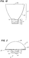
- optical element 2 is an optical concentrator.
- Fig. 1D provides an example of an optical concentrator bonded to LED die 4.
- Fig. 1D depicts side surface 23 of the optical concentrator (optical element 2) as having a parabolic shape, side surface 23 may have any shape designed to concentrate light, such as a cone-shape or a beveled shape, and according to the invention, side surface 23 is coated with a reflective metallization or a reflective dielectric material.
- Active layer 12 of LED die 4 is positioned to reduce the amount of light that experiences total internal reflection at surface 24.
- active layer 12 may be distributed about the focal point of optical element 2.
- a photon which would have intersected surface 24 at an angle greater than the critical angle in the absence of surface 23 intersects surface 24 at an angle within the critical angle if it first reflects off surface 23. Therefore, surface 23 increases the likelihood of a photon escaping LED die 4.
- optical element 2 is a graded index optical element having, for example, a refractive index decreasing in the direction perpendicular to surface 22 or decreasing radially from a maximum near a center of surface 22.
- Optical element 2 includes, in one implementation, luminescent material that converts light of wavelengths emitted by active region 12 to other wavelengths.
- a coating on surface 22, for example includes luminescent material.
- the luminescent material includes, for example, conventional phosphor particles, organic semiconductors, II-VI or III-V semiconductors, II-VI or III-V semiconductor quantum dots or nanocrystals, dyes, polymers, and materials such as GaN that luminesce from defect centers.
- a region of optical element 2 near surface 22 is doped, for example, with a luminescent material.
- n bond ⁇ n LED ⁇ n optical element but either n bond > n epoxy or bonding layer 6 is thin as described above, then, neglecting Fresnel reflection losses, more light is extracted into optical element 2 than would be extracted into an epoxy encapsulant or air.
- n bond ⁇ n optical element ⁇ n LED but either n bond > n epoxy or bonding layer 6 is thin as described above and n optical element > n epoxy then, neglecting Fresnel reflection losses, more light is extracted into optical element 2 than would be extracted into an epoxy encapsulant or air.
- transparent optical element 2 has a refractive index at the emission wavelengths of LED die 4 greater than 1.5, more preferably greater than about 1.8.
- the ambient medium is air (n air ⁇ 1) rather than an epoxy encapsulant, with n air substituted for n epoxy .
- bonding layer 6 includes phosphor particles and the refractive index of the bonding material, preferably a high index chalcogenide glass, approximately matches the refractive index of the phosphor particles, then scattering by the phosphor particles of light emitted by the active region or by the phosphor particles will be negligible.
- the refractive indices of the phosphor particles, the bonding material, the top layer (for example n-layer 8) of LED die 4, and the optical element are all about equal. This is the case if the top layer of LED die 4 is InGaN, the phosphor particles are SrS:Eu and/or SrGaS:Eu, and the optical element is ZnS.
- transparent optical element 2 is bonded directly to a top surface 18 of LED die 4 without the use of a separate bonding layer.
- the inventors believe that a bond is effected between optical element 2 and LED die 4 by, for example, material transfer via shear stress, evaporation-condensation, liquification (or melting or softening) followed by solidification, diffusion, or alloying.
- Metallization layer 20, if present, is patterned to allow surface 22 of optical element 2 to directly contact surface 18.
- Surface 22 is optionally also patterned by etching, for example.
- transparent optical element 2 is formed from a material, such as those listed above, which could be used to form a separate bonding layer.
- the material from which the top layer of LED die 4 (for example, n-layer 8 in Fig. 2 ) is formed is suitable as a bonding material.
- a bonding material for example, n-layer 8 in Fig. 2
- the interface of optical element 2 and LED die 4 at surface 18, for example is a bonded interface characterized by mass transfer between optical element 2 and LED die 4.
- Transparent optical element 2 is directly bonded to LED die 4, not being part of the invention, at temperatures and pressures as described above for the bonding process utilizing bonding layer 6.
- surface 18 of LED die 4 or surface 22 of optical element 2 is doped with a material exhibiting a high diffusivity such as, for example, Zn or Si. Such doping can be accomplished during materials growth by MOCVD, VPE, LPE or MBE, for example, or after materials growth by, for example, implantation.
- a thin layer of a high diffusivity material is disposed between optical element 2 and LED die 4 by deposition on at least one of surfaces 18 and 22. Deposition can be accomplished, for example, by conventional means such as evaporation or sputtering.
- the amount of high diffusivity material used should be sufficiently low to maintain the transparency of, for example, optical element 2 and the top layer of LED die 4.
- transparent optical element 2 may be a block of transparent optical element material that is bonded to LED die 4 in the manner described above, and then formed into optical element 2.
- Optical element 2 may be formed using etching, perhaps in conjunction with photolithography or other lithographic techniques, electron beam lithography, ion beam lithography, X-ray lithography, or holographic lithography. Wet or dry chemical etching techniques such as plasma etching, reactive ion etching (RIE), and chemically-assisted ion beam etching (CAIBE) may be used as well.
- optical element 2 may be milled into a surface of the transparent optical element material using ion beam milling or focused ion beam milling (FIB), ablated into the surface with a scanning electron or a laser beam, or mechanically machined into the surface by sawing, milling, or scribing.
- optical element 2 may be stamped into the block of transparent optical element material using the method disclosed in U.S. Patent Application Serial No. 09/823,841 .
- LED die 4 it is advantageous to bond LED die 4 to optical element 2 rather than to conventionally encase LED die 4 in an encapsulant.
- the light extraction efficiency through surface 18 of LED die 4 bonded to optical element 2 with bonding layer 6, as described above, is improved compared to a conventional epoxy encapsulated LED.
- LED die 4 need not be subject to the damaging stress experienced by epoxy encapsulated (encased) LEDs.
- LED die 4 can be run at higher temperatures. Consequently, the light output of LED die 4 can be increased by running the LED at higher current densities.
- LED die 4 bonded to optical element 2 could be additionally encapsulated in, for example, epoxy or silicone. Such encapsulation of LED die 4 bonded to optical element 2 would not effect the light extraction efficiency through surface 18 of LED die 4 into optical element 2. Total internal reflection at the interface of surface 24 and the encapsulant would be minimized, as described above, by the shape and size of optical element 2.
- LED die 4 includes, for example, metallization for electrical contacts that degrades at elevated temperatures.
- LED die 4 is bonded to a submount, not shown, with solders or silver bearing die-attach epoxies that degrade at high temperatures. (Note that die-attach epoxy is to be distinguished from an epoxy encapsulant.) Consequently, in one implementation the process of bonding optical element 2 to LED die 4, with a bonding layer 6, occurs at temperatures less than about 500°C in order to avoid, for example, degrading the metallization or the die-attach epoxy.
- optical element 2 is bonded to an incomplete LED die, for example, an LED die missing some or all metallization. In the latter implementation, fabrication of the LED die is completed after the optical element bonding process.
- the structure of LED die 4 may differ from the structure depicted in Figs. 1A, 1B, 1C , 1D, and 2 .
- Like reference numbers in Figs. 1A, 1B, 1C , 1D, 2 , 3, 4 , 5, 6, 7, 8 , 9, 10, and 11 designate the same parts in the various examples.
- sides 26 and 28 of LED die 4 are beveled such that they intersect bonding layer 6 at angles. Though two beveled sides are shown in Fig. 3 , in other examples LED die 4 has more or less than two beveled sides and is, for example, substantially conical or pyramidal in shape.
- Beveled sides 26 and 28 reflect light emitted from active region 12 toward bonding layer 6. Light that might otherwise have been trapped in LED die 4 or lost out the sides of the die is thereby advantageously extracted through bonding layer 6 and optical element 2.
- LED die 4 is surrounded by a low refractive index medium such as air, and a portion of the light incident on beveled sides 26 and 28 from active region 12 is totally internally reflected toward bonding layer 6.
- beveled sides 26 and 28 are coated with a reflective coating, in one implementation a metal layer and in another implementation a dielectric layer, that reflects light toward bonding layer 6.
- contact 16 is highly reflective. Accordingly, in this example light incident on contact 16 is reflected toward bonding layer 6 and optical element 2 either directly or after additional reflection from side 26 or side 28. The light extraction efficiency of LED die 4 is consequently increased.
- LED die 4 includes conducting transparent superstrate 30 electrically coupled to metallization layer 20 and electrically coupled to n-layer 8, and conducting, optionally transparent, substrate 32 electrically coupled to p-layer 10 and to contact 16.
- Superstrate 30 and (optionally) substrate 32 are formed, for example, from semiconductors having a band gap energy greater than the energy of photons emitted by LED die 4.
- Superstrate 30 is formed from a material having an index of refraction at the emission wavelengths of active region 12 preferably greater than about 1.5, more preferably greater than about 1.8.
- sides 26 and 28 of LED die 4 are beveled and highly reflective and contact 16 is highly reflective, as described above.
- transparent optical element 2 is bonded to superstrate 30 with bonding layer 6, and n-layer 8 is electrically coupled to metallization layer 20 by n-contact 14.
- transparent optical element 2 is directly bonded to superstrate 30 and n-contact 14 is not separately provided.
- Contact 14 and contact 16 are disposed on the same side of LED die 4 in the "flip chip" examples, not being part of the invention, illustrated in Figs. 6 and 7 . Since optical element 2 is bonded to the opposite side of LED die 4 from contacts 14 and 16, no metallization layer is required on optical element 2 in these examples. The light extraction efficiency into optical element 2 is improved by the absence of the metallization layer. In other implementations, sides 26 and 28 of LED die 4 are beveled and highly reflective and contact 16 is highly reflective, as described above.
- Transparent superstrate 34 is formed from a material such as, for example, sapphire, SiC, GaN, or GaP, having an index of refraction at the emission wavelengths of active region 12 preferably greater than about 1.5, more preferably greater than about 1.8.
- optical element 2 is bonded with bonding layer 6 to transparent superstrate 34.
- optical element 2 is directly bonded to transparent superstrate 34.
- optical element 2 is formed from ZnS
- superstrate 34 is formed from SiC or GaN
- n-layer 8 is formed from a III-Nitride semiconductor such as GaN.
- optical element 2 is formed from GaP
- superstrate 34 is formed from GaP
- n-layer 8 is formed from a III-Phosphide semiconductor such as an AlInGaP alloy.
- transparent bonding layer 6 is formed, for example, from ZnS.
- n-layer 8, p-layer 10, and active region 12 is substantially perpendicular to optical element 2.
- no metallization layer is required on optical element 2.
- optical element 2 is bonded with bonding layer 6 to LED die 4.
- optical element 2 is directly bonded to LED die 4.
- LED die 4 is sawn ("diced") from a wafer with cuts made in a direction substantially perpendicular to layers 8 and 10 and to active region 12.
- the surface of LED die 4 to be bonded to optical element 2 is optionally polished to reduce its roughness.
- sides 26 and 28 of LED die 4 are beveled, contact 14 and contact 16 are highly reflective, and reflective layer 36 is located to reflect light into optical element 2.
- LED die 4 is located in a recess 38 in surface 22 of optical element 2 to which LED die 4 is bonded.
- optical element 2 is directly bonded to LED die 4.
- optical element 2 is bonded to LED die 4 with bonding layer 6.
Landscapes
- Led Devices (AREA)
- Led Device Packages (AREA)
- Exposure And Positioning Against Photoresist Photosensitive Materials (AREA)
Description
- The present invention relates to light emitting diodes with enhanced light extraction efficiency.
- The light extraction efficiency of a light emitting diode (LED) is defined as the ratio of the LED's external quantum efficiency to the LED's internal quantum efficiency. Typically, the light extraction efficiency of a packaged LED is substantially less than one, i.e., much of the light generated in the LED's active region never reaches the external environment.
- Light extraction efficiency is reduced by total internal reflection at interfaces between the LED and surrounding material followed by reabsorption of the totally internally reflected light in the LED. For example, for a cubic geometry LED on a transparent substrate encapsulated in epoxy, the refractive index (n) at the emission wavelength changes from a value of, for example, nsemi ∼3.5 in the LED semiconductor to nepoxy ∼1.5 in the epoxy. The corresponding critical angle for total internal reflection of light incident on the epoxy encapsulant from the LED semiconductor of this example is θC = arcsin(nepoxy/nsemi) ∼25°. Neglecting scattering and multiple reflections, light emitted over 4π steradians from a point in the active region of the cubic LED crosses a semiconductor / epoxy encapsulant interface only if it is emitted into one of six narrow light cones, one for each interface, with each light cone having a half angle equal to the critical angle. Additional losses due to total internal reflection can occur at the epoxy / air interface. Consequently, an efficient conventional geometry (for example, rectangular parallelepiped) transparent substrate AlInGaP LED encapsulated in epoxy, for example, may have an external quantum efficiency of only ∼40%, despite having an internal quantum efficiency of nearly 100 %.
- The effect of total internal reflection on the light extraction efficiency of LEDs is further discussed in
U.S. Patents 5,779,924 ;5,793,062 ; and6,015,719 . - In one approach to improving light extraction efficiency, LEDs are ground into hemispherical shapes. Light emitted from a point in the active region of a hemispherically shaped LED intersects the hemispherical interface at near normal incidence. Thus, total internal reflection is reduced. However, this technique is tedious and wasteful of material. In addition, defects introduced during the grinding process may compromise the reliability and performance of the LEDs.
- In another approach, LEDs are encapsulated (encased) in a material with a dome or hemispherically shaped surface. For example, the epoxy encapsulant of the above example may be dome shaped to reduce losses due to total internal reflection at the epoxy encapsulant / air interface. However, shaping the surface of a low refractive index encapsulant such as epoxy does not reduce losses due to total internal reflection at the semiconductor / low index encapsulant interface. Moreover, epoxy encapsulants typically have coefficients of thermal expansion that poorly match those of the semiconductor materials in the LED. Consequently, the epoxy encapsulant subjects the LED to mechanical stress upon heating or cooling and may damage the LED. LEDs are also encapsulated in dome shaped high index glasses, which increase the critical angle for the semiconductor / encapsulant interface. Unfortunately, optical absorption in high index glasses and mechanical stress typically degrade the performance of a LED encapsulated in such glass.
-
JP H10-151794 A WO 00/39860 A1 US 2001/0000209 A1 disclose an optical concentrator with a reflective coating on a side surface which is bonded to a LED chip.US 5,698,452 discloses a total internal reflector bonded to a LED chip. -
EP 0616376A1 andGB 2326023 A - What is needed is a device for increasing the light extraction efficiency of light emitting diodes which does not suffer from the drawbacks of previous devices.
- The light emitting device of the invention is defined in claim 1. Preferred embodiments of the light emitting device of the invention are defined by the dependent claims.
- Light emitting devices with improved light extraction efficiency are provided. The LED die has a stack of layers including semiconductor layers comprising an active region. The stack is bonded to a transparent optical element.
- In some examples, not being part of the invention, the optical element is a lens, for example a hemispheric lens or a Fresnel lens. According to the invention, the optical element is an optical concentrator having a side surface coated with a reflective metallization or a reflective dielectric material. The optical element is formed, from optical glass, III-V semiconductors, II-VI semiconductors, group IV semiconductors and compounds, metal oxides, metal fluorides, diamond, sapphire, yttrium aluminum garnet, or combinations thereof. The refractive index of the optical element for light emitted from the active region is preferably greater than about 1.5, more preferably greater than about 1.8.
- In one example, not being part of the invention, the transparent optical element is directly bonded to at least one of the semiconductor layers of the stack. In another example, not being part of the invention, the transparent optical element is directly bonded to a transparent superstrate disposed above the semiconductor layers. The transparent superstrate preferably has a refractive index for light emitted from the active region greater than about 1.8.
- According to the invention, the light emitting device includes a transparent bonding layer disposed between the optical element and a surface of the stack. The transparent bonding layer bonds the optical element to the surface of the stack. According to the invention, the surface includes a surface of one of the semiconductor layers. In another example, not being part of the invention, the surface includes a surface of a transparent superstrate layer disposed above the semiconductor layers. According to the invention, the transparent bonding layer is formed from phosphide compounds, arsenide compounds, antimonide compounds, nitride compounds, or from a material selected from the group consisting of: metal fluorides, diamond, sapphire, yttrium aluminum garnet, and combinations thereof. According to the invention, the transparent bonding material has an index of refraction for light emitted from the active region greater than 1.5, preferably greater than about 1.8.
- An example of a method, not being part of the invention, of bonding a transparent optical element to a LED die having a stack of layers including semiconductor layers comprising an active region is provided. The method includes elevating a temperature of the optical element and the stack and applying a pressure to press the optical element and the stack together. In one example, the method also includes disposing a layer of a transparent bonding material between the stack and the optical element. The bonding method can be applied to a pre-made optical element or to a block of optical element material which is later formed or shaped into an optical element such as a lens or an optical concentrator.
- Bonding a high refractive index optical element to a LED die improves the light extraction efficiency of the light emitting device by reducing loss due to total internal reflection. Advantageously, this improvement can be achieved without the use of an encapsulant.
-
Fig. 1A is a schematic diagram of an optical element and a LED die to be bonded to each other, not being part of the invention. -
Fig. 1B is a schematic diagram of an optical element bonded with a bonding layer to a LED die, not being part of the invention. -
Fig. 1C is a schematic diagram of an optical element bonded to a LED die, not being part of the invention. -
Fig. 1D is a schematic diagram of an optical concentrator bonded to a LED die in accordance with the present invention. -
Fig. 2 is a schematic diagram of an optical element directly bonded to a LED die, not being part of the invention. -
Fig. 3 is a schematic diagram of an optical element bonded with a bonding layer to a LED die having beveled sides, not being part of the invention. -
Fig. 4 is a schematic diagram of an optical element bonded with a bonding layer to a LED die having substrate and superstrate layers, not being part of the invention. -
Fig. 5 is a schematic diagram of an optical element directly bonded to a LED die having substrate and superstrate layers, not being part of the invention. -
Fig. 6 is a schematic diagram of an optical element bonded with a bonding layer to a LED die having a "flip chip" geometry, not being part of the present invention. -
Fig. 7 is a schematic diagram of an optical element directly bonded to a LED die having a "flip chip" geometry, not being part of the invention. -
Fig. 8 is a schematic diagram of an optical element bonded with a bonding layer to a LED die having an active region substantially perpendicular to the optical element, not being part of the invention. -
Fig. 9 is a schematic diagram of an optical element bonded directly to a LED die having an active region substantially perpendicular to the optical element, not being part of the invention. -
Fig. 10 is a schematic diagram of a LED die located in a recess of a surface of an optical element to which it is directly bonded, not being part of the invention. -
Fig. 11 is a schematic diagram of a LED die located in a recess of a surface of an optical element to which it is bonded with a bonding layer, not being part of the invention. -
Fig. 1A depicts a transparentoptical element 2 and aLED die 4 to be bonded to each other, not being part of the invention. - In
Fig. 1B , in accordance with an example, not being part of the invention, transparentoptical element 2 is bonded to LED die 4 with atransparent bonding layer 6. - The term "transparent" is used herein to indicate that an optical element so described, such as a "transparent optical element," a "transparent bonding layer," a "transparent substrate," or a "transparent superstrate" transmits light at the emission wavelengths of the LED with less than about 50%, preferably less than about 10%, single pass loss due to absorption or scattering. The emission wavelengths of the LED may lie in the infrared, visible, or ultraviolet regions of the electromagnetic spectrum. One of ordinary skill in the art will recognize that the conditions "less than 50% single pass loss" and "less than 10% single pass loss" may be met by various combinations of transmission path length and absorption constant. As used herein, "optical concentrator" means optical elements having a side surface coated with a reflective metal or a reflective dielectric material to reflect or redirect incident light.
- LED die 4 illustrated in
Figs. 1A and 1B includes afirst semiconductor layer 8 of n-type conductivity (n-layer) and asecond semiconductor layer 10 of p-type conductivity (p-layer). Semiconductor layers 8 and 10 are electrically coupled toactive region 12.Active region 12 is, for example, a p-n diode junction associated with the interface oflayers active region 12 includes one or more semiconductor layers that are doped n-type or p-type or are undoped. N-contact 14 and p-contact 16 are electrically coupled tosemiconductor layers Active region 12 emits light upon application of a suitable voltage acrosscontacts layers 8 and 9, together withcontacts layer 8 is a p-type layer, contact 14 is a p-contact,layer 10 is an n-type layer, andcontact 16 is an n-contact. - Semiconductor layers 8 and 10 and
active region 12 are formed from III-V semiconductors including but not limited to AlN, AlP, AlAs, AlSb, GaN, GaP, GaAs, GaSb, InN, InP, InAs, InSb, II-VI semiconductors including but not limited to ZnS, ZnSe, CdSe, CdTe, group IV semiconductors including but not limited to Ge, Si, SiC, and mixtures or alloys thereof. These semiconductors have indices of refraction ranging from about 2.4 to about 4.1 at the typical emission wavelengths of LEDs in which they are present. For example, III-Nitride semiconductors such as GaN have refractive indices of about 2.4 at 500 nm, and III-Phosphide semiconductors such as InGaP have refractive indices of about 3.7 at 600 nm. -
Contacts contacts - Although
Figs. 1A and 1B illustrate a particular LED structure, the present invention is independent of the number of semiconductor layers in LED die 4, and independent of the detailed structure ofactive region 12. It should be noted that dimensions of the various elements of LED die 4 illustrated in the various figures are not to scale. - In one example, not being part of the invention, a layer of bonding material is applied to a
top surface 18 of LED die 4 (Fig. 1A ) to form transparent bonding layer 6 (Fig. 1B ) with which to bondoptical element 2 to LED die 4.Transparent bonding layer 6 is, for example, about 1 nm (10 Å) to about 100 microns (µm) thick. The bonding material is applied, for example, by conventional deposition techniques including but not limited to sputtering, evaporation, chemical vapor deposition (CVD), or as part of material growth by, for example, metal-organic chemical vapor deposition (MOCVD), vapor phase epitaxy (VPE), liquid phase epitaxy (LPE), or molecular beam epitaxy (MBE).Transparent bonding layer 6 is optionally patterned with, for example, conventional photolithographic and etching techniques to leavecontact 14 uncovered by bonding material and thus to permitcontact 14 to make electrical contact withoptional metallization layer 20 onoptical element 2.Metallization layer 20, in one embodiment a mesh and in other embodiments a continuous or patterned layer, for example, about 0.2 nm (2 Å) to about 500 nm (5000 Å) thick, transmits greater than about 10%, preferably greater than about 50%, of incident light and provides a physically accessible electrical contact coupled to contact 14.Metallization layer 20 is formed, for example, from metals or transparent conductors such as indium tin oxide. - In an alternative example,
transparent bonding layer 6 is formed on substantiallyflat surface 22 ofoptical element 2 or on the surface ofmetallization layer 20 and optionally patterned with, for example, conventional photolithographic and etching techniques to permit electrical contact betweencontact 14 andmetallization layer 20. In another embodiment transparent bonding layers such asbonding layer 6 are formed on bothsurface 18 of LED die 4 and surface 22 ofoptical element 2. In other embodiments, contact 14 is not separately provided, andbonding layer 6 is patterned to permit electrical contact betweenmetallization layer 20 and n-layer 8. In the example shown inFig. 1C , not being part of the invention, neithercontact 14 norbonding layer 6 is separately provided, andmetallization layer 20 additionally functions as a bonding layer. In other examples, contact 14 is not located onsurface 18 and themetallization layer 20 is not used. - Though the following discussion assumes that
bonding layer 6 is formed on LED die 4 rather than onsurface 22 ofoptical element 2 or on both LED die 4 andsurface 22, the process described below can be simply modified to implement the latter examples. - In one implementation, not being part of the invention, the bonding material from which
transparent bonding layer 6 is formed is a high index optical glass, i.e, an optical glass having a refractive index greater than about 1.5 in the range of wavelengths emitted byactive region 12. Preferably, the refractive index is greater than about 1.8.Transparent bonding layer 6 is formed, for example, from Schott glass SF59, a dense flint glass which has refractive index (n) ∼1.95 at ∼600 nanometers (nm) and a glass transition temperature (To) ∼362°C. Alternatively,transparent bonding layer 6 is formed from high index optical glasses including but not limited to Schott glass LaSF 3, with n ∼1.81 at ∼600 nm and TG ∼630°C; Schott glass LaSF N18, with n ∼1.91 at ∼600 nm and To ∼660°C; and mixtures thereof. These glasses are available from Schott Glass Technologies Incorporated, of Duryea, PA.Bonding layer 6 may also be formed from a high index chalcogenide glass, such as (Ge,Sb,Ga)(S,Se) chalcogenide glasses, for example. - In other implementations, not being part of the invention,
bonding layer 6 is formed from III-V semiconductors including but not limited to GaP (n ∼ 3.3 at 600 nm), InGaP (n ∼ 3.7 at 600 nm), GaAs (n ∼ 3.4 at 500 nm), and GaN(n ∼ 2.4 at 500 nm); II-VI semiconductors including but not limited to ZnS (n ∼ 2.4 at 500 nm), ZnSe (n ∼ 2.6 at 500 nm), ZnTe (n ∼ 3.1 at 500 nm), CdS (n ∼ 2.6 at 500 nm), CdSe (n ∼ 2.6 at 500 nm), and CdTe (n ∼ 2.7 at 500 nm); group IV semiconductors and compounds including but not limited to Si (n ∼ 3.5 at 500 nm), and Ge (n ∼ 4.1 at 500 nm); organic semiconductors, metal oxides including but not limited to tungsten oxide, titanium oxide (n ∼ 2.9 at 500 nm), nickel oxide (n ∼ 2.2 at 500 nm), zirconium oxide (n ∼ 2.2 at 500 nm), indium tin oxide, and chromium oxide. - In accordance with the invention,
bonding layer 6 is formed from metal fluorides, diamond, sapphire, yttrium aluminum garnet (YAG), or combinations thereof, or from phosphide compounds, arsenide compounds, antimonide compounds or nitride compounds. -
Bonding layer 6 includes, in one implementation, luminescent material that converts light of wavelengths emitted byactive region 12 to other wavelengths. The luminescent material includes, for example, conventional phosphor particles, organic semiconductors, II-VI or III-V semiconductors, II-VI or III-V semiconductor quantum dots or nanocrystals, dyes, polymers, and materials such as GaN that luminesce from defect centers. Ifbonding layer 6 includes conventional phosphor particles, then bondinglayer 6 should be thick enough to accommodate particles typically having a size of about 5 microns to about 50 microns. - In accordance with the invention,
bonding layer 6 is formed from a material having a refractive index at the LED's emission wavelengths greater than 1.5, preferably greater than about 1.8, and preferably having a refractive index less than that of the top layer of LED die 4, for example,semiconductor layer 8. Hence, a critical angle exists for total internal reflection of light incident on thesemiconductor layer 8 /bonding layer 6 interface from inside LED die 4. This critical angle is increased compared to the critical angle for an interface between LED die 4 and epoxy or air, however, and more light is extracted throughsurface 18 intobonding layer 6 than would be extracted into an epoxy encapsulant or air. In another implementation, the refractive index ofbonding layer 6 is greater than or equal to that of semiconductor layer 8 (for example, GaN), and none of the light incident onbonding layer 6 from inside LED die 4 is totally internally reflected. Neglecting Fresnel reflection losses, which can be minimized by approximately matching the refractive indices ofbonding layer 6 and the top layer of LED die 4, in the latter case also more light is extracted throughsurface 18 intobonding layer 6 than would be extracted into an epoxy encapsulant or air. - In another example, not being part of the invention,
transparent bonding layer 6 is formed from a low index bonding material, i.e., a bonding material having a refractive index less than 1.5 at the LED's emission wavelengths. Magnesium fluoride, for example, is one such bonding material. Low index optical glasses, epoxies, and silicones may also be suitable low index bonding materials. One of ordinary skill in the art will recognize that efficient transmission of light from LED die 4 acrosstransparent bonding layer 6, formed from a low index material, tooptical element 2 can be achieved ifbonding layer 6 is sufficiently thin. Accordingly, in this example losses due to total internal reflection at the LED die 4 /bonding layer 6 interface are reduced by making the thickness ofbonding layer 6 less than about 50 nm (500 Å), preferably less than about 10 nm (100 Å).Optical element 2 might bond poorly to LED die 4 if the roughness ofsurface 18 orsurface 22 or typical height of irregularities onsurface 18 orsurface 22 exceed the thickness ofbonding layer 6. In this example, surfaces 18 and 22 are optionally polished to achieve a surface roughness of magnitude less than or equal to the thickness ofbonding layer 6. - If LED die 4 includes material that absorbs light emitted by
active region 12, and ifbonding layer 6 is formed from a low index material but is not thin as described above, then a large portion of the light emitted byactive region 12 will typically be trapped in LED die 4 and lost to absorption even ifbonding layer 6 is itself nonabsorbing. In contrast, abonding layer 6 formed from a high index material will typically couple a larger fraction of light emitted byactive region 12 out of LED die 4 intooptical element 2, even if the high index bonding material is a material such as a chalcogenide glass, for example, which absorbs a portion of the emitted light. - After
transparent bonding layer 6 is applied to LED die 4, the substantiallyflat surface 22 ofoptical element 2 is placed againstbonding layer 6. The temperature ofbonding layer 6 is then raised to a temperature between about room temperature and about 1000°C, andoptical element 2 and LED die 4 are pressed together for a period of time of about one second to about 6 hours at a pressure of about 1 pound per square inch (psi) to about 6000 psi. The inventors believe that in this processoptical element 2 is bonded to LED die 4 by a bond effected betweenoptical element 2 and bonding layer 6 (formed on LED die 4) by, for example, material transfer via shear stress, evaporation-condensation, liquification (or melting or softening) followed by solidification, diffusion, or alloying. The inventors believe that in other implementationsoptical element 2 is bonded to LED die 4 by a bond similarly effected by, for example, material transfer between bonding layers formed on each ofoptical element 2 and LED die 4 or between bonding layer 6 (formed on optical element 2) and LED die 4. Thus, a bonded interface characterized by material transfer may be disposed betweenoptical element 2 and LED die 4. In one example,surface 18 at the interface of n-layer 8 andbonding layer 6 is such a bonded interface. In another implementation, an interface of bonding layers formed on each ofoptical element 2 and LED die 4 is a bonded interface. In another example, an interface ofoptical element 2 andbonding layer 6 is a bonded interface. - If
transparent bonding layer 6 is formed on LED die 4 from an optical glass, not being part of the invention, then the temperature ofbonding layer 6 is raised to about the strain point temperature of the optical glass. The strain point temperature, which is near to but less than the glass transition temperature (To), is the temperature at which the optical glass has a viscosity of about 1014.5 poises. The strain point temperature also corresponds to the first nonlinearity in a plot of expansion versus temperature for the optical glass, and thus represents the lower limit of the annealing range. The resulting flexibility and lowered surface tension of the optical glass inlayer 6 at temperatures near or above the strain point temperature allow the optical glass to microscopically conform to surface 22 and to effect a bond betweenoptical element 2 andbonding layer 6. - The process of bonding
optical element 2 to LED die 4 described above may be performed with devices disclosed inU.S. Patents 5,502,316 and5,376,580 , previously used to bond semiconductor wafers to each other at elevated temperatures and pressures. The disclosed devices may be modified to accommodate LED dice and optical elements, as necessary. Alternatively, the bonding process described above may be performed with a conventional vertical press. - Transparent
optical element 2 is formed, for example, from SiC (n ∼ 2.7 at 500 nm), aluminum oxide (sapphire, n ∼ 1.8 at 500 nm) or diamond (n ∼ 2.4 at 500 nm). A severe mismatch between the thermal expansion coefficients ofoptical element 2 and LED die 4 to whichoptical element 2 is bonded can causeoptical element 2 to detach from LED die 4 upon heating or cooling. Also, approximately matching thermal expansion coefficients reduces the stress induced in LED die 4 bybonding layer 6 andoptical element 2. Hence, in one implementationoptical element 2 is formed from a material having a thermal expansion coefficient approximately matching the thermal expansion coefficient of LED die 4 to whichoptical element 2 is bonded. - In one embodiment, transparent
optical element 2 has a shape and a size such that light enteringoptical element 2 from LED die 4 will intersectsurface 24 ofoptical element 2 at angles of incidence near normal incidence. Total internal reflection at the interface ofsurface 24 and the ambient medium, typically air, is thereby reduced. In addition, since the range of angles of incidence is narrow, Fresnel reflection losses atsurface 24 can be reduced by applying aconventional antireflection coating 25 to surface 24. The shape ofoptical element 2 is, in examples not being part of the invention, a portion of a sphere such as a hemisphere, a Weierstrass sphere (truncated sphere), a portion of a sphere less than a hemisphere or a portion of an ellipsoid such as a truncated ellipsoid. The angles of incidence atsurface 24 for light enteringoptical element 2 from LED die 4 more closely approach normal incidence as the size ofoptical element 2 is increased. Hence, the smallest ratio of a length of the base of transparentoptical element 2 to a length of thesurface 18 of LED die 4 is preferably greater than about 1, more preferably greater than about 2. - One of ordinary skill in the art will recognize that the maximum size for which an
optical element 2 of a particular material continues to be transparent as defined above is determined by the absorption constant of the optical element material at the emission wavelengths of the LED. In one example, not being part of the invention,optical element 2 is a Fresnel lens. Fresnel lenses are typically thinner than, for example, spherical optical elements of comparable focal lengths, and hence are less absorptive. - According to the invention,
optical element 2 is an optical concentrator.Fig. 1D provides an example of an optical concentrator bonded to LED die 4. AlthoughFig. 1D depictsside surface 23 of the optical concentrator (optical element 2) as having a parabolic shape,side surface 23 may have any shape designed to concentrate light, such as a cone-shape or a beveled shape, and according to the invention,side surface 23 is coated with a reflective metallization or a reflective dielectric material.Active layer 12 of LED die 4 is positioned to reduce the amount of light that experiences total internal reflection atsurface 24. For example,active layer 12 may be distributed about the focal point ofoptical element 2. A photon which would have intersectedsurface 24 at an angle greater than the critical angle in the absence ofsurface 23 intersects surface 24 at an angle within the critical angle if it first reflects offsurface 23. Therefore, surface 23 increases the likelihood of a photon escapingLED die 4. - In yet another implementation,
optical element 2 is a graded index optical element having, for example, a refractive index decreasing in the direction perpendicular to surface 22 or decreasing radially from a maximum near a center ofsurface 22. -
Optical element 2 includes, in one implementation, luminescent material that converts light of wavelengths emitted byactive region 12 to other wavelengths. In another example, not being part of the invention, a coating onsurface 22, for example, includes luminescent material. The luminescent material includes, for example, conventional phosphor particles, organic semiconductors, II-VI or III-V semiconductors, II-VI or III-V semiconductor quantum dots or nanocrystals, dyes, polymers, and materials such as GaN that luminesce from defect centers. Alternatively, a region ofoptical element 2 nearsurface 22 is doped, for example, with a luminescent material. - The magnitudes of the refractive indices of optical element 2 (noptical element), bonding layer 6 (nbond), and the top layer of LED die 4 (nLED) can be ordered in six permutations. If nLED ≤ nbond ≤ noptical element or nLED ≤ noptical element ≤ nbond, then losses due to total internal reflection are eliminated, but Fresnel losses may occur. In particular, if nLED = nbond = noptical element, then light enters
optical element 2 from LED die 4 without losses due to Fresnel or total internal reflection. Alternatively, if nbond ≤ nLED ≤ noptical element but either nbond > nepoxy orbonding layer 6 is thin as described above, then, neglecting Fresnel reflection losses, more light is extracted intooptical element 2 than would be extracted into an epoxy encapsulant or air. Similarly, if nbond ≤ noptical element ≤ nLED but either nbond > nepoxy orbonding layer 6 is thin as described above and noptical element > nepoxy, then, neglecting Fresnel reflection losses, more light is extracted intooptical element 2 than would be extracted into an epoxy encapsulant or air. If noptical element ≤ nbond ≤ nLED or noptical element ≤ nLED ≤ nbond but noptical element > nepoxy, then, neglecting Fresnel reflection losses, more light is extracted intooptical element 2 than would be extracted into an epoxy encapsulant or air. Thus, according to the invention, transparentoptical element 2 has a refractive index at the emission wavelengths of LED die 4 greater than 1.5, more preferably greater than about 1.8. A similar analysis applies if the ambient medium is air (nair ∼1) rather than an epoxy encapsulant, with nair substituted for nepoxy. - If
bonding layer 6 includes phosphor particles and the refractive index of the bonding material, preferably a high index chalcogenide glass, approximately matches the refractive index of the phosphor particles, then scattering by the phosphor particles of light emitted by the active region or by the phosphor particles will be negligible. Preferably, the refractive indices of the phosphor particles, the bonding material, the top layer (for example n-layer 8) of LED die 4, and the optical element are all about equal. This is the case if the top layer of LED die 4 is InGaN, the phosphor particles are SrS:Eu and/or SrGaS:Eu, and the optical element is ZnS. - Referring to
Fig. 2 , in an example not being part of the invention, transparentoptical element 2 is bonded directly to atop surface 18 of LED die 4 without the use of a separate bonding layer. The inventors believe that a bond is effected betweenoptical element 2 and LED die 4 by, for example, material transfer via shear stress, evaporation-condensation, liquification (or melting or softening) followed by solidification, diffusion, or alloying.Metallization layer 20, if present, is patterned to allowsurface 22 ofoptical element 2 to directly contactsurface 18.Surface 22 is optionally also patterned by etching, for example. In one example, transparentoptical element 2 is formed from a material, such as those listed above, which could be used to form a separate bonding layer. In another example not being part of the invention, the material from which the top layer of LED die 4 (for example, n-layer 8 inFig. 2 ) is formed is suitable as a bonding material. Thus eitheroptical element 2 or a top layer of LED die 4 functions additionally as a bonding layer, and no separate bonding layer is necessary. In one example, not being part of the invention, the interface ofoptical element 2 and LED die 4 atsurface 18, for example, is a bonded interface characterized by mass transfer betweenoptical element 2 and LED die 4. - For
optical element 2 directly bonded to LED die 4, not being part of the invention, if nLED ≤ noptical element or if noptical element < nLED but noptical element > nepoxy, then, neglecting Fresnel reflection losses, more light is extracted intooptical element 2 than would be extracted into an epoxy encapsulant. A similar analysis applies if the ambient medium is air (nair ∼1) rather than an epoxy encapsulant, with nair substituted for nepoxy. - Transparent
optical element 2 is directly bonded to LED die 4, not being part of the invention, at temperatures and pressures as described above for the bonding process utilizingbonding layer 6. In one example,surface 18 of LED die 4 or surface 22 ofoptical element 2 is doped with a material exhibiting a high diffusivity such as, for example, Zn or Si. Such doping can be accomplished during materials growth by MOCVD, VPE, LPE or MBE, for example, or after materials growth by, for example, implantation. In another example, a thin layer of a high diffusivity material is disposed betweenoptical element 2 and LED die 4 by deposition on at least one ofsurfaces optical element 2 and LED die 4 and enhances material transfer betweenoptical element 2 and LED die 4. The amount of high diffusivity material used should be sufficiently low to maintain the transparency of, for example,optical element 2 and the top layer of LED die 4. - Application of the bonding method is not limited to a pre-made optical element. Rather, transparent
optical element 2 may be a block of transparent optical element material that is bonded to LED die 4 in the manner described above, and then formed intooptical element 2.Optical element 2 may be formed using etching, perhaps in conjunction with photolithography or other lithographic techniques, electron beam lithography, ion beam lithography, X-ray lithography, or holographic lithography. Wet or dry chemical etching techniques such as plasma etching, reactive ion etching (RIE), and chemically-assisted ion beam etching (CAIBE) may be used as well. Also,optical element 2 may be milled into a surface of the transparent optical element material using ion beam milling or focused ion beam milling (FIB), ablated into the surface with a scanning electron or a laser beam, or mechanically machined into the surface by sawing, milling, or scribing. In addition,optical element 2 may be stamped into the block of transparent optical element material using the method disclosed inU.S. Patent Application Serial No. 09/823,841 . - It is advantageous to bond LED die 4 to
optical element 2 rather than to conventionally encase LED die 4 in an encapsulant. For example, the light extraction efficiency throughsurface 18 of LED die 4 bonded tooptical element 2 withbonding layer 6, as described above, is improved compared to a conventional epoxy encapsulated LED. In addition, LED die 4 need not be subject to the damaging stress experienced by epoxy encapsulated (encased) LEDs. Moreover, in the absence of epoxy encapsulants, which degrade at relatively low temperatures, LED die 4 can be run at higher temperatures. Consequently, the light output of LED die 4 can be increased by running the LED at higher current densities. - If desired, however, LED die 4 bonded to
optical element 2 could be additionally encapsulated in, for example, epoxy or silicone. Such encapsulation of LED die 4 bonded tooptical element 2 would not effect the light extraction efficiency throughsurface 18 of LED die 4 intooptical element 2. Total internal reflection at the interface ofsurface 24 and the encapsulant would be minimized, as described above, by the shape and size ofoptical element 2. - In some implementations, LED die 4 includes, for example, metallization for electrical contacts that degrades at elevated temperatures. In other implementations, LED die 4 is bonded to a submount, not shown, with solders or silver bearing die-attach epoxies that degrade at high temperatures. (Note that die-attach epoxy is to be distinguished from an epoxy encapsulant.) Consequently, in one implementation the process of bonding
optical element 2 to LED die 4, with abonding layer 6, occurs at temperatures less than about 500°C in order to avoid, for example, degrading the metallization or the die-attach epoxy. In another implementation,optical element 2 is bonded to an incomplete LED die, for example, an LED die missing some or all metallization. In the latter implementation, fabrication of the LED die is completed after the optical element bonding process. - As
Figs. 3, 4 ,5, 6 ,7, 8 ,9, 10, and 11 illustrate, the structure of LED die 4 may differ from the structure depicted inFigs. 1A, 1B, 1C ,1D, and 2 . Like reference numbers inFigs. 1A, 1B, 1C ,1D, 2 ,3, 4 ,5, 6, 7, 8 ,9, 10, and 11 designate the same parts in the various examples. - In the example of
Fig. 3 , not being part of the invention, sides 26 and 28 of LED die 4 are beveled such that they intersectbonding layer 6 at angles. Though two beveled sides are shown inFig. 3 , in other examples LED die 4 has more or less than two beveled sides and is, for example, substantially conical or pyramidal in shape. -
Beveled sides active region 12 towardbonding layer 6. Light that might otherwise have been trapped in LED die 4 or lost out the sides of the die is thereby advantageously extracted throughbonding layer 6 andoptical element 2. In one example, LED die 4 is surrounded by a low refractive index medium such as air, and a portion of the light incident onbeveled sides active region 12 is totally internally reflected towardbonding layer 6. In another example, beveled sides 26 and 28 are coated with a reflective coating, in one implementation a metal layer and in another implementation a dielectric layer, that reflects light towardbonding layer 6. - In one example, contact 16 is highly reflective. Accordingly, in this example light incident on
contact 16 is reflected towardbonding layer 6 andoptical element 2 either directly or after additional reflection fromside 26 orside 28. The light extraction efficiency of LED die 4 is consequently increased. - In the examples illustrated in
Figs. 4 and5 , not being part of the invention, LED die 4 includes conductingtransparent superstrate 30 electrically coupled tometallization layer 20 and electrically coupled to n-layer 8, and conducting, optionally transparent,substrate 32 electrically coupled to p-layer 10 and to contact 16. Superstrate 30 and (optionally)substrate 32 are formed, for example, from semiconductors having a band gap energy greater than the energy of photons emitted by LED die 4.Superstrate 30 is formed from a material having an index of refraction at the emission wavelengths ofactive region 12 preferably greater than about 1.5, more preferably greater than about 1.8. In other implementations, sides 26 and 28 of LED die 4 are beveled and highly reflective andcontact 16 is highly reflective, as described above. In the example illustrated inFig. 4 , transparentoptical element 2 is bonded to superstrate 30 withbonding layer 6, and n-layer 8 is electrically coupled tometallization layer 20 by n-contact 14. In the example illustrated inFig. 5 , transparentoptical element 2 is directly bonded tosuperstrate 30 and n-contact 14 is not separately provided. -
Contact 14 andcontact 16 are disposed on the same side of LED die 4 in the "flip chip" examples, not being part of the invention, illustrated inFigs. 6 and 7 . Sinceoptical element 2 is bonded to the opposite side of LED die 4 fromcontacts optical element 2 in these examples. The light extraction efficiency intooptical element 2 is improved by the absence of the metallization layer. In other implementations, sides 26 and 28 of LED die 4 are beveled and highly reflective andcontact 16 is highly reflective, as described above.Transparent superstrate 34 is formed from a material such as, for example, sapphire, SiC, GaN, or GaP, having an index of refraction at the emission wavelengths ofactive region 12 preferably greater than about 1.5, more preferably greater than about 1.8. In the example illustrated inFig. 6 ,optical element 2 is bonded withbonding layer 6 totransparent superstrate 34. In the example illustrated inFig. 7 ,optical element 2 is directly bonded totransparent superstrate 34. - In one implementation of the examples illustrated in
Figs. 6 and 7 ,optical element 2 is formed from ZnS,superstrate 34 is formed from SiC or GaN, and n-layer 8 is formed from a III-Nitride semiconductor such as GaN. In another implementation,optical element 2 is formed from GaP,superstrate 34 is formed from GaP, and n-layer 8 is formed from a III-Phosphide semiconductor such as an AlInGaP alloy. If present,transparent bonding layer 6 is formed, for example, from ZnS. - In the examples not being part of the invention, illustrated in
Figs. 8 and9 , the orientation of n-layer 8, p-layer 10, andactive region 12 is substantially perpendicular tooptical element 2. As in the examples illustrated inFigs. 6 and 7 , no metallization layer is required onoptical element 2. In the example illustrated inFig. 8 ,optical element 2 is bonded withbonding layer 6 to LED die 4. In the example illustrated inFig. 9 ,optical element 2 is directly bonded to LED die 4. In one implementation, LED die 4 is sawn ("diced") from a wafer with cuts made in a direction substantially perpendicular tolayers active region 12. In this implementation, the surface of LED die 4 to be bonded tooptical element 2 is optionally polished to reduce its roughness. In other implementations, sides 26 and 28 of LED die 4 are beveled, contact 14 andcontact 16 are highly reflective, andreflective layer 36 is located to reflect light intooptical element 2. - In the examples, not being part of the invention, of
Figs. 10 and 11 , LED die 4 is located in arecess 38 insurface 22 ofoptical element 2 to which LED die 4 is bonded. In the example illustrated inFig. 10 ,optical element 2 is directly bonded to LED die 4. In the example ofFig. 11 ,optical element 2 is bonded to LED die 4 withbonding layer 6. - While the present invention is illustrated with particular embodiments, the invention is intended to include all variations and modifications falling within the scope of the invention as defined by the appended claims.
Claims (15)
- A light emitting device comprising a light emitting diode die (4) formed by a stack of layers including semiconductor layers (8, 10, 12) comprising an active region (12), said device further comprising a transparent optical element (2) bonded by a transparent bonding layer (6) to a surface of said stack,
wherein,said optical element is an optical concentrator, said optical concentrator having a side surface (23) coated with a reflective metallization or a reflective dielectric material,said surface of said stack includes a surface of one of said semiconductor layers,said transparent bonding layer has an index of refraction greater than 1.5 for light emitted by said active region,said transparent bonding layer is formed from a material selected from the group consisting of metal fluorides, diamond, sapphire, yttrium aluminum garnet, andcombinations thereof, or from phosphide compounds, arsenide compounds, antimonide compounds or nitride compounds, andsaid optical concentrator is formed from a material selected from the group consisting of optical glass, III-V semiconductors, II-VI semiconductors, group IV semiconductors and compounds, metal oxides, metal fluorides, diamond, sapphire, yttrium aluminum garnet, and combinations thereof. - The light emitting device of claim 1, wherein said side surface (23) is a parabolic side surface.
- The light emitting device of claim 1, wherein said side surface (23) is a cone-shaped side surface.
- The light emitting device of claim 1, wherein said side surface (23) is a beveled side surface.
- The light emitting device of claim 1, wherein said transparent bonding layer (6) includes a luminescent material that converts light of wavelengths emitted by said active region (12) to other wavelengths.
- The light emitting device of claim 1, wherein said optical concentrator (2) is formed from a material selected from the group consisting of zirconium oxide, sapphire, GaP, ZnS, and SiC.
- The light emitting device of claim 1, wherein said optical concentrator (2) includes one or more luminescent materials that convert light of a wavelength emitted by said active region (12) to at least another wavelength.
- The light emitting device of claim 1, wherein a smallest ratio of a length of a base of said optical concentrator (2) to a length of said surface of said stack is greater than one.
- The light emitting device of claim 8, wherein said ratio is greater than two.
- The light emitting device of claim 1, wherein a refractive index of said optical concentrator (2) for light emitted by said active region (12) is greater than 1.5.
- The light emitting device of claim 10, wherein said refractive index of said optical concentrator (2) for light emitted by said active region (12) is greater than 1.8.
- The light emitting device of claim 1, wherein a refractive index of said optical concentrator (2) is greater than or equal to a refractive index of said semiconductor layers (8, 10, 12) for light emitted by said active region (12).
- The light emitting device of claim 1, wherein said stack comprises at least one beveled side (26, 28) located to reflect light emitted from said active region (12) toward said optical concentrator (2).
- The light emitting device of claim 1, wherein said index of refraction of said transparent bonding layer (6) is greater than 1.8 for light emitted by said active region (12).
- The light emitting device of claim 1, wherein said transparent bonding layer (6) has a thickness less than 50 nm.
Applications Claiming Priority (2)
| Application Number | Priority Date | Filing Date | Title |
|---|---|---|---|
| US880204 | 2001-06-12 | ||
| US09/880,204 US7064355B2 (en) | 2000-09-12 | 2001-06-12 | Light emitting diodes with improved light extraction efficiency |
Publications (3)
| Publication Number | Publication Date |
|---|---|
| EP1267420A2 EP1267420A2 (en) | 2002-12-18 |
| EP1267420A3 EP1267420A3 (en) | 2009-04-22 |
| EP1267420B1 true EP1267420B1 (en) | 2019-04-10 |
Family
ID=25375720
Family Applications (1)
| Application Number | Title | Priority Date | Filing Date |
|---|---|---|---|
| EP01204002.8A Expired - Lifetime EP1267420B1 (en) | 2001-06-12 | 2001-10-19 | Light emitting diodes with improved light extraction efficiency |
Country Status (4)
| Country | Link |
|---|---|
| US (1) | US7064355B2 (en) |
| EP (1) | EP1267420B1 (en) |
| KR (1) | KR100941639B1 (en) |
| TW (1) | TW569469B (en) |
Families Citing this family (171)
| Publication number | Priority date | Publication date | Assignee | Title |
|---|---|---|---|---|
| JP2002141556A (en) | 2000-09-12 | 2002-05-17 | Lumileds Lighting Us Llc | Light-emitting diode with improved light extraction effect |
| US7053419B1 (en) * | 2000-09-12 | 2006-05-30 | Lumileds Lighting U.S., Llc | Light emitting diodes with improved light extraction efficiency |
| DE10054966A1 (en) * | 2000-11-06 | 2002-05-16 | Osram Opto Semiconductors Gmbh | Component for optoelectronics |
| DE10101554A1 (en) * | 2001-01-15 | 2002-08-01 | Osram Opto Semiconductors Gmbh | emitting diode |
| US6746889B1 (en) * | 2001-03-27 | 2004-06-08 | Emcore Corporation | Optoelectronic device with improved light extraction |
| US6987613B2 (en) * | 2001-03-30 | 2006-01-17 | Lumileds Lighting U.S., Llc | Forming an optical element on the surface of a light emitting device for improved light extraction |
| US6839362B2 (en) * | 2001-05-22 | 2005-01-04 | Saint-Gobain Ceramics & Plastics, Inc. | Cobalt-doped saturable absorber Q-switches and laser systems |
| US8545629B2 (en) | 2001-12-24 | 2013-10-01 | Crystal Is, Inc. | Method and apparatus for producing large, single-crystals of aluminum nitride |
| JP3896027B2 (en) * | 2002-04-17 | 2007-03-22 | シャープ株式会社 | Nitride-based semiconductor light-emitting device and method for manufacturing the same |
| US6870311B2 (en) * | 2002-06-07 | 2005-03-22 | Lumileds Lighting U.S., Llc | Light-emitting devices utilizing nanoparticles |
| DE10234977A1 (en) * | 2002-07-31 | 2004-02-12 | Osram Opto Semiconductors Gmbh | Radiation-emitting thin layer semiconductor component comprises a multiple layer structure based on gallium nitride containing an active radiation-producing layer and having a first main surface and a second main surface |
| CA2517009A1 (en) * | 2003-02-26 | 2004-09-10 | Cree, Inc. | White light source using emitting diode and phosphor and method of fabrication |
| DE10319274A1 (en) * | 2003-04-29 | 2004-12-02 | Osram Opto Semiconductors Gmbh | light source |
| US6921912B2 (en) | 2003-06-03 | 2005-07-26 | Micron Technology, Inc. | Diode/superionic conductor/polymer memory structure |
| US6803607B1 (en) | 2003-06-13 | 2004-10-12 | Cotco Holdings Limited | Surface mountable light emitting device |
| US7147352B2 (en) | 2003-06-23 | 2006-12-12 | Howmedica Leibinger, Inc. | Precision light emitting device |
| US7009213B2 (en) * | 2003-07-31 | 2006-03-07 | Lumileds Lighting U.S., Llc | Light emitting devices with improved light extraction efficiency |
| US7326477B2 (en) * | 2003-09-23 | 2008-02-05 | Saint-Gobain Ceramics & Plastics, Inc. | Spinel boules, wafers, and methods for fabricating same |
| US20050061230A1 (en) * | 2003-09-23 | 2005-03-24 | Saint-Gobain Ceramics & Plastics, Inc. | Spinel articles and methods for forming same |
| US7045223B2 (en) * | 2003-09-23 | 2006-05-16 | Saint-Gobain Ceramics & Plastics, Inc. | Spinel articles and methods for forming same |
| US8604497B2 (en) * | 2003-09-26 | 2013-12-10 | Osram Opto Semiconductors Gmbh | Radiation-emitting thin-film semiconductor chip |
| JP4093943B2 (en) * | 2003-09-30 | 2008-06-04 | 三洋電機株式会社 | LIGHT EMITTING ELEMENT AND MANUFACTURING METHOD THEREOF |
| US7408566B2 (en) * | 2003-10-22 | 2008-08-05 | Oki Data Corporation | Semiconductor device, LED print head and image-forming apparatus using same, and method of manufacturing semiconductor device |
| DE10351397A1 (en) * | 2003-10-31 | 2005-06-16 | Osram Opto Semiconductors Gmbh | LED chip |
| DE10351349A1 (en) * | 2003-10-31 | 2005-06-16 | Osram Opto Semiconductors Gmbh | Production of a luminescent diode chip applies a radiation decoupling surface and a semiconductor body with an epitaxial-grown sequence of semiconductor layers with an active zone |
| US7090357B2 (en) * | 2003-12-23 | 2006-08-15 | 3M Innovative Properties Company | Combined light source for projection display |
| JP2005209795A (en) * | 2004-01-21 | 2005-08-04 | Koito Mfg Co Ltd | Light emitting module and lamp |
| US7300177B2 (en) * | 2004-02-11 | 2007-11-27 | 3M Innovative Properties | Illumination system having a plurality of light source modules disposed in an array with a non-radially symmetrical aperture |
| US7427146B2 (en) * | 2004-02-11 | 2008-09-23 | 3M Innovative Properties Company | Light-collecting illumination system |
| US7246923B2 (en) * | 2004-02-11 | 2007-07-24 | 3M Innovative Properties Company | Reshaping light source modules and illumination systems using the same |
| US7250715B2 (en) * | 2004-02-23 | 2007-07-31 | Philips Lumileds Lighting Company, Llc | Wavelength converted semiconductor light emitting devices |
| US10575376B2 (en) | 2004-02-25 | 2020-02-25 | Lynk Labs, Inc. | AC light emitting diode and AC LED drive methods and apparatus |
| WO2011143510A1 (en) | 2010-05-12 | 2011-11-17 | Lynk Labs, Inc. | Led lighting system |
| US10499465B2 (en) | 2004-02-25 | 2019-12-03 | Lynk Labs, Inc. | High frequency multi-voltage and multi-brightness LED lighting devices and systems and methods of using same |
| TWI244221B (en) * | 2004-03-01 | 2005-11-21 | Epistar Corp | Micro-reflector containing flip-chip light emitting device |
| US7361938B2 (en) | 2004-06-03 | 2008-04-22 | Philips Lumileds Lighting Company Llc | Luminescent ceramic for a light emitting device |
| US20070267646A1 (en) * | 2004-06-03 | 2007-11-22 | Philips Lumileds Lighting Company, Llc | Light Emitting Device Including a Photonic Crystal and a Luminescent Ceramic |
| US8294166B2 (en) | 2006-12-11 | 2012-10-23 | The Regents Of The University Of California | Transparent light emitting diodes |
| US7553683B2 (en) * | 2004-06-09 | 2009-06-30 | Philips Lumiled Lighting Co., Llc | Method of forming pre-fabricated wavelength converting elements for semiconductor light emitting devices |
| GB2416041A (en) * | 2004-07-08 | 2006-01-11 | Innovium Res Ltd | Optical device for the transmission and/or collection of optical signals |
| US7390097B2 (en) * | 2004-08-23 | 2008-06-24 | 3M Innovative Properties Company | Multiple channel illumination system |
| KR101080355B1 (en) | 2004-10-18 | 2011-11-04 | 삼성전자주식회사 | Light emitting diode, lens for the same |
| US20060091414A1 (en) * | 2004-10-29 | 2006-05-04 | Ouderkirk Andrew J | LED package with front surface heat extractor |
| US7304425B2 (en) * | 2004-10-29 | 2007-12-04 | 3M Innovative Properties Company | High brightness LED package with compound optical element(s) |
| US20060091412A1 (en) * | 2004-10-29 | 2006-05-04 | Wheatley John A | Polarized LED |
| US7329982B2 (en) * | 2004-10-29 | 2008-02-12 | 3M Innovative Properties Company | LED package with non-bonded optical element |
| US20060091411A1 (en) * | 2004-10-29 | 2006-05-04 | Ouderkirk Andrew J | High brightness LED package |
| US7419839B2 (en) * | 2004-11-12 | 2008-09-02 | Philips Lumileds Lighting Company, Llc | Bonding an optical element to a light emitting device |
| US7462502B2 (en) | 2004-11-12 | 2008-12-09 | Philips Lumileds Lighting Company, Llc | Color control by alteration of wavelength converting element |
| US7314770B2 (en) * | 2004-11-18 | 2008-01-01 | 3M Innovative Properties Company | Method of making light emitting device with silicon-containing encapsulant |
| US7192795B2 (en) * | 2004-11-18 | 2007-03-20 | 3M Innovative Properties Company | Method of making light emitting device with silicon-containing encapsulant |
| US20060105483A1 (en) * | 2004-11-18 | 2006-05-18 | Leatherdale Catherine A | Encapsulated light emitting diodes and methods of making |
| CN101438406B (en) * | 2004-11-19 | 2011-04-20 | 皇家飞利浦电子股份有限公司 | Light emitting device with inorganic housing |
| US9070850B2 (en) | 2007-10-31 | 2015-06-30 | Cree, Inc. | Light emitting diode package and method for fabricating same |
| US7919815B1 (en) | 2005-02-24 | 2011-04-05 | Saint-Gobain Ceramics & Plastics, Inc. | Spinel wafers and methods of preparation |
| WO2006099171A2 (en) * | 2005-03-11 | 2006-09-21 | The Arizona Boar Of Regents, A Body Corporate Acting On Behalf Of Arizona State University | NOVEL GeSiSn-BASED COMPOUNDS, TEMPLATES, AND SEMICONDUCTOR STRUCTURES |
| US8748923B2 (en) * | 2005-03-14 | 2014-06-10 | Philips Lumileds Lighting Company Llc | Wavelength-converted semiconductor light emitting device |
| EP1862035B1 (en) * | 2005-03-14 | 2013-05-15 | Koninklijke Philips Electronics N.V. | Phosphor in polycrystalline ceramic structure and a light-emitting element comprising same |
| US7341878B2 (en) * | 2005-03-14 | 2008-03-11 | Philips Lumileds Lighting Company, Llc | Wavelength-converted semiconductor light emitting device |
| WO2006117710A1 (en) * | 2005-04-29 | 2006-11-09 | Koninklijke Philips Electronics N.V. | Light source with glass housing |
| JP2006324324A (en) * | 2005-05-17 | 2006-11-30 | Sumitomo Electric Ind Ltd | Light emitting device, method for manufacturing light emitting device, and nitride semiconductor substrate |
| US7445340B2 (en) * | 2005-05-19 | 2008-11-04 | 3M Innovative Properties Company | Polarized, LED-based illumination source |
| DE112005003581T5 (en) * | 2005-05-20 | 2008-04-03 | Cree, Inc. | White LED with high efficiency |
| US8669572B2 (en) | 2005-06-10 | 2014-03-11 | Cree, Inc. | Power lamp package |
| JP2007012682A (en) * | 2005-06-28 | 2007-01-18 | Shinka Jitsugyo Kk | Manufacturing method of optical module |
| US20070092737A1 (en) * | 2005-10-21 | 2007-04-26 | 3M Innovative Properties Company | Method of making light emitting device with silicon-containing encapsulant |
| US20070092736A1 (en) * | 2005-10-21 | 2007-04-26 | 3M Innovative Properties Company | Method of making light emitting device with silicon-containing encapsulant |
| US7595515B2 (en) * | 2005-10-24 | 2009-09-29 | 3M Innovative Properties Company | Method of making light emitting device having a molded encapsulant |
| WO2007050484A1 (en) * | 2005-10-24 | 2007-05-03 | 3M Innovative Properties Company | Method of making light emitting device having a molded encapsulant |
| US7641735B2 (en) | 2005-12-02 | 2010-01-05 | Crystal Is, Inc. | Doped aluminum nitride crystals and methods of making them |
| US7772604B2 (en) | 2006-01-05 | 2010-08-10 | Illumitex | Separate optical device for directing light from an LED |
| US7717343B2 (en) * | 2006-01-12 | 2010-05-18 | Hand Held Products, Inc. | High-efficiency illumination in data collection devices |
| RU2008133603A (en) * | 2006-01-16 | 2010-02-27 | Конинклейке Филипс Электроникс Н.В. (Nl) | LIGHT-RADIATING DEVICE WITH EU-CONTAINING CRYSTALLOPHOSPHORUS |
| US8101961B2 (en) * | 2006-01-25 | 2012-01-24 | Cree, Inc. | Transparent ohmic contacts on light emitting diodes with growth substrates |
| US7675145B2 (en) | 2006-03-28 | 2010-03-09 | Cree Hong Kong Limited | Apparatus, system and method for use in mounting electronic elements |
| US9034103B2 (en) | 2006-03-30 | 2015-05-19 | Crystal Is, Inc. | Aluminum nitride bulk crystals having high transparency to ultraviolet light and methods of forming them |
| CN101427388B (en) * | 2006-04-24 | 2010-08-18 | 旭硝子株式会社 | Light emitting device |
| US8748915B2 (en) | 2006-04-24 | 2014-06-10 | Cree Hong Kong Limited | Emitter package with angled or vertical LED |
| US7635915B2 (en) | 2006-04-26 | 2009-12-22 | Cree Hong Kong Limited | Apparatus and method for use in mounting electronic elements |
| US20070257270A1 (en) * | 2006-05-02 | 2007-11-08 | 3M Innovative Properties Company | Led package with wedge-shaped optical element |
| US20070257271A1 (en) * | 2006-05-02 | 2007-11-08 | 3M Innovative Properties Company | Led package with encapsulated converging optical element |
| US7953293B2 (en) * | 2006-05-02 | 2011-05-31 | Ati Technologies Ulc | Field sequence detector, method and video device |
| US7525126B2 (en) | 2006-05-02 | 2009-04-28 | 3M Innovative Properties Company | LED package with converging optical element |
| US7390117B2 (en) * | 2006-05-02 | 2008-06-24 | 3M Innovative Properties Company | LED package with compound converging optical element |
| US7423297B2 (en) * | 2006-05-03 | 2008-09-09 | 3M Innovative Properties Company | LED extractor composed of high index glass |
| US8141384B2 (en) * | 2006-05-03 | 2012-03-27 | 3M Innovative Properties Company | Methods of making LED extractor arrays |
| KR100736623B1 (en) | 2006-05-08 | 2007-07-09 | 엘지전자 주식회사 | Vertical light emitting device and manufacturing method |
| US20070269586A1 (en) * | 2006-05-17 | 2007-11-22 | 3M Innovative Properties Company | Method of making light emitting device with silicon-containing composition |
| US7655486B2 (en) * | 2006-05-17 | 2010-02-02 | 3M Innovative Properties Company | Method of making light emitting device with multilayer silicon-containing encapsulant |
| JP2009540616A (en) * | 2006-06-12 | 2009-11-19 | スリーエム イノベイティブ プロパティズ カンパニー | LED device having re-emitting semiconductor structure and focusing optical element |
| US20070284565A1 (en) * | 2006-06-12 | 2007-12-13 | 3M Innovative Properties Company | Led device with re-emitting semiconductor construction and optical element |
| US7952110B2 (en) * | 2006-06-12 | 2011-05-31 | 3M Innovative Properties Company | LED device with re-emitting semiconductor construction and converging optical element |
| US7902542B2 (en) * | 2006-06-14 | 2011-03-08 | 3M Innovative Properties Company | Adapted LED device with re-emitting semiconductor construction |
| WO2008011377A2 (en) * | 2006-07-17 | 2008-01-24 | 3M Innovative Properties Company | Led package with converging extractor |
| US8735920B2 (en) | 2006-07-31 | 2014-05-27 | Cree, Inc. | Light emitting diode package with optical element |
| US8367945B2 (en) | 2006-08-16 | 2013-02-05 | Cree Huizhou Opto Limited | Apparatus, system and method for use in mounting electronic elements |
| US8092735B2 (en) | 2006-08-17 | 2012-01-10 | 3M Innovative Properties Company | Method of making a light emitting device having a molded encapsulant |
| JP2008059645A (en) * | 2006-08-30 | 2008-03-13 | Hitachi Ltd | Recording head |
| KR101370367B1 (en) * | 2006-09-22 | 2014-03-05 | 코닌클리케 필립스 엔.브이. | Light emitting device with tension relaxation |
| US7745843B2 (en) * | 2006-09-26 | 2010-06-29 | Stanley Electric Co., Ltd. | Semiconductor light emitting device |
| WO2008042351A2 (en) * | 2006-10-02 | 2008-04-10 | Illumitex, Inc. | Led system and method |
| US20090275157A1 (en) * | 2006-10-02 | 2009-11-05 | Illumitex, Inc. | Optical device shaping |
| JP2010510671A (en) * | 2006-11-17 | 2010-04-02 | スリーエム イノベイティブ プロパティズ カンパニー | Optical adhesive composition for LED light source |
| EP2087533A2 (en) * | 2006-11-17 | 2009-08-12 | 3M Innovative Properties Company | Planarized led with optical extractor |
| WO2008064081A2 (en) * | 2006-11-17 | 2008-05-29 | 3M Innovative Properties Company | High efficiency light emitting diodes and methods of forming the same |
| JP4561732B2 (en) * | 2006-11-20 | 2010-10-13 | トヨタ自動車株式会社 | Mobile positioning device |
| WO2008063884A1 (en) * | 2006-11-20 | 2008-05-29 | 3M Innovative Properties Company | Optical bonding composition for led light source |
| US7902564B2 (en) * | 2006-12-22 | 2011-03-08 | Koninklijke Philips Electronics N.V. | Multi-grain luminescent ceramics for light emitting devices |
| US9771666B2 (en) | 2007-01-17 | 2017-09-26 | Crystal Is, Inc. | Defect reduction in seeded aluminum nitride crystal growth |
| WO2008088838A1 (en) | 2007-01-17 | 2008-07-24 | Crystal Is, Inc. | Defect reduction in seeded aluminum nitride crystal growth |
| US8080833B2 (en) | 2007-01-26 | 2011-12-20 | Crystal Is, Inc. | Thick pseudomorphic nitride epitaxial layers |
| US9711703B2 (en) | 2007-02-12 | 2017-07-18 | Cree Huizhou Opto Limited | Apparatus, system and method for use in mounting electronic elements |
| US7618163B2 (en) * | 2007-04-02 | 2009-11-17 | Ruud Lighting, Inc. | Light-directing LED apparatus |
| US9484499B2 (en) * | 2007-04-20 | 2016-11-01 | Cree, Inc. | Transparent ohmic contacts on light emitting diodes with carrier substrates |
| US20080258130A1 (en) * | 2007-04-23 | 2008-10-23 | Bergmann Michael J | Beveled LED Chip with Transparent Substrate |
| US20090026471A1 (en) * | 2007-07-27 | 2009-01-29 | Noeton Optoelectronics Corp. | Light-scattering structure, light emitting device comprising the same and method of forming the same |
| DE102008021403A1 (en) * | 2007-09-28 | 2009-04-02 | Osram Opto Semiconductors Gmbh | Optoelectronic semiconductor body and method for its production |
| DE102007049799A1 (en) * | 2007-09-28 | 2009-04-02 | Osram Opto Semiconductors Gmbh | Optoelectronic component |
| DE102008005345A1 (en) * | 2007-09-28 | 2009-04-02 | Osram Opto Semiconductors Gmbh | Semiconductor-based device, semiconductor device-based device receptacle, and method of making a semiconductor-based device |
| US11317495B2 (en) | 2007-10-06 | 2022-04-26 | Lynk Labs, Inc. | LED circuits and assemblies |
| US11297705B2 (en) | 2007-10-06 | 2022-04-05 | Lynk Labs, Inc. | Multi-voltage and multi-brightness LED lighting devices and methods of using same |
| US10256385B2 (en) | 2007-10-31 | 2019-04-09 | Cree, Inc. | Light emitting die (LED) packages and related methods |
| JP2011512037A (en) | 2008-02-08 | 2011-04-14 | イルミテックス, インコーポレイテッド | System and method for emitter layer shaping |
| US8388193B2 (en) | 2008-05-23 | 2013-03-05 | Ruud Lighting, Inc. | Lens with TIR for off-axial light distribution |
| US9423096B2 (en) | 2008-05-23 | 2016-08-23 | Cree, Inc. | LED lighting apparatus |
| US8348475B2 (en) | 2008-05-23 | 2013-01-08 | Ruud Lighting, Inc. | Lens with controlled backlight management |
| DE102008025756B4 (en) * | 2008-05-29 | 2023-02-23 | OSRAM Opto Semiconductors Gesellschaft mit beschränkter Haftung | semiconductor device |
| WO2010001306A1 (en) * | 2008-07-01 | 2010-01-07 | Koninklijke Philips Electronics N.V. | Wavelength converted light emitting diode with reduced emission of unconverted light |
| US7841750B2 (en) | 2008-08-01 | 2010-11-30 | Ruud Lighting, Inc. | Light-directing lensing member with improved angled light distribution |
| US7741134B2 (en) * | 2008-09-15 | 2010-06-22 | Bridgelux, Inc. | Inverted LED structure with improved light extraction |
| US20100097821A1 (en) * | 2008-10-16 | 2010-04-22 | Osram Sylvania, Inc. | Light emitting diode-based lamp having a volume scattering element |
| US8791471B2 (en) | 2008-11-07 | 2014-07-29 | Cree Hong Kong Limited | Multi-chip light emitting diode modules |
| KR101154758B1 (en) * | 2008-11-18 | 2012-06-08 | 엘지이노텍 주식회사 | Semiconductor light emitting device and LED package having the same |
| TW201034256A (en) | 2008-12-11 | 2010-09-16 | Illumitex Inc | Systems and methods for packaging light-emitting diode devices |
| US8368112B2 (en) | 2009-01-14 | 2013-02-05 | Cree Huizhou Opto Limited | Aligned multiple emitter package |
| KR100969146B1 (en) * | 2009-02-18 | 2010-07-08 | 엘지이노텍 주식회사 | Semiconductor light emitting device and fabrication method thereof |
| US9255686B2 (en) | 2009-05-29 | 2016-02-09 | Cree, Inc. | Multi-lens LED-array optic system |
| US8449128B2 (en) | 2009-08-20 | 2013-05-28 | Illumitex, Inc. | System and method for a lens and phosphor layer |
| US8585253B2 (en) | 2009-08-20 | 2013-11-19 | Illumitex, Inc. | System and method for color mixing lens array |
| US20110062469A1 (en) | 2009-09-17 | 2011-03-17 | Koninklijke Philips Electronics N.V. | Molded lens incorporating a window element |
| US12279345B2 (en) | 2009-12-28 | 2025-04-15 | Lynk Labs, Inc. | Light emitting diode and LED drive apparatus |
| JP5806734B2 (en) | 2010-06-30 | 2015-11-10 | クリスタル アイエス, インコーポレーテッドCrystal Is, Inc. | Large single crystal growth of aluminum nitride by thermal gradient control |
| TWI512807B (en) * | 2011-06-09 | 2015-12-11 | 晶元光電股份有限公司 | Semiconductor component structure and separation method thereof |
| US8962359B2 (en) * | 2011-07-19 | 2015-02-24 | Crystal Is, Inc. | Photon extraction from nitride ultraviolet light-emitting devices |
| US20140239809A1 (en) | 2011-08-18 | 2014-08-28 | Lynk Labs, Inc. | Devices and systems having ac led circuits and methods of driving the same |
| WO2013043844A1 (en) * | 2011-09-20 | 2013-03-28 | The Regents Of The University Of California | Light emitting diode with conformal surface electrical contacts with glass encapsulation |
| US8564004B2 (en) | 2011-11-29 | 2013-10-22 | Cree, Inc. | Complex primary optics with intermediate elements |
| US9247597B2 (en) | 2011-12-02 | 2016-01-26 | Lynk Labs, Inc. | Color temperature controlled and low THD LED lighting devices and systems and methods of driving the same |
| GB201202222D0 (en) | 2012-02-09 | 2012-03-28 | Mled Ltd | Enhanced light extraction |
| US10408429B2 (en) | 2012-02-29 | 2019-09-10 | Ideal Industries Lighting Llc | Lens for preferential-side distribution |
| US9541257B2 (en) | 2012-02-29 | 2017-01-10 | Cree, Inc. | Lens for primarily-elongate light distribution |
| US9541258B2 (en) | 2012-02-29 | 2017-01-10 | Cree, Inc. | Lens for wide lateral-angle distribution |
| DE102012102476B4 (en) * | 2012-03-22 | 2022-09-08 | OSRAM Opto Semiconductors Gesellschaft mit beschränkter Haftung | Process for producing an optoelectronic semiconductor component |
| USD697664S1 (en) | 2012-05-07 | 2014-01-14 | Cree, Inc. | LED lens |
| US9054235B2 (en) * | 2013-01-22 | 2015-06-09 | Micron Technology, Inc. | Solid-state transducer devices with optically-transmissive carrier substrates and related systems, methods, and devices |
| USD718490S1 (en) | 2013-03-15 | 2014-11-25 | Cree, Inc. | LED lens |
| US9299880B2 (en) | 2013-03-15 | 2016-03-29 | Crystal Is, Inc. | Pseudomorphic electronic and optoelectronic devices having planar contacts |
| US20140367816A1 (en) * | 2013-06-12 | 2014-12-18 | Avago Technologies General Ip (Singapore) Pte.Ltd. | Photodetector device having light-collecting optical microstructure |
| CN104241262B (en) | 2013-06-14 | 2020-11-06 | 惠州科锐半导体照明有限公司 | Light emitting device and display device |
| US9523479B2 (en) | 2014-01-03 | 2016-12-20 | Cree, Inc. | LED lens |
| JP6817187B2 (en) | 2014-07-23 | 2021-01-20 | クリスタル アイエス, インコーポレーテッドCrystal Is, Inc. | Lighting equipment assembly and baking methods, and lighting equipment |
| US10622522B2 (en) | 2014-09-05 | 2020-04-14 | Theodore Lowes | LED packages with chips having insulated surfaces |
| BR102016004795B1 (en) * | 2015-03-05 | 2021-09-08 | Nichia Corporation | LIGHT EMITTING DIODE |
| DE102016114341A1 (en) * | 2016-08-03 | 2018-02-08 | HELLA GmbH & Co. KGaA | Light module with at least one semiconductor light source and with at least one optical body |
| US10886437B2 (en) * | 2016-11-03 | 2021-01-05 | Lumileds Llc | Devices and structures bonded by inorganic coating |
| US10468566B2 (en) | 2017-04-10 | 2019-11-05 | Ideal Industries Lighting Llc | Hybrid lens for controlled light distribution |
| US11079077B2 (en) | 2017-08-31 | 2021-08-03 | Lynk Labs, Inc. | LED lighting system and installation methods |
| US10797207B2 (en) | 2018-07-30 | 2020-10-06 | Lumileds Llc | Light emitting device with porous structure to enhance color point shift as a function of drive current |
| US10756242B2 (en) | 2018-07-30 | 2020-08-25 | Lumileds Llc | Light-emitting device with light scatter tuning to control color shift |
| CN109786975B (en) * | 2019-01-25 | 2020-10-09 | 西安电子科技大学 | A realization device of OAM vortex electromagnetic wave orbit plane omnidirectional radiation |
| US12514030B2 (en) * | 2021-10-14 | 2025-12-30 | Lumileds Singapore Pte. Ltd. | Narrowband reflector for micro-LED arrays |
Citations (5)
| Publication number | Priority date | Publication date | Assignee | Title |
|---|---|---|---|---|
| EP0616376A1 (en) * | 1993-03-19 | 1994-09-21 | Hewlett-Packard Company | Wafer bonding of light emitting diode layers |
| US5698452A (en) * | 1994-04-25 | 1997-12-16 | Lucent Technologies Inc. | Method of making integrated detector/photoemitter with non-imaging director |
| GB2326023A (en) * | 1997-06-03 | 1998-12-09 | Hewlett Packard Co | Semiconductor light-emitting device |
| WO2000039860A1 (en) * | 1998-12-29 | 2000-07-06 | Vasily Ivanovich Shveikin | Injection non-coherent emitter |
| JP2000218862A (en) * | 1999-02-03 | 2000-08-08 | Ricoh Co Ltd | Array light emitting device |
Family Cites Families (60)
| Publication number | Priority date | Publication date | Assignee | Title |
|---|---|---|---|---|
| US3769536A (en) | 1972-01-28 | 1973-10-30 | Varian Associates | Iii-v photocathode bonded to a foreign transparent substrate |
| US3964157A (en) * | 1974-10-31 | 1976-06-22 | Bell Telephone Laboratories, Incorporated | Method of mounting semiconductor chips |
| US4109054A (en) | 1976-05-19 | 1978-08-22 | Ferro Corporation | Composites of glass-ceramic-to-metal, seals and method of making same |
| JPS5565473A (en) | 1978-11-13 | 1980-05-16 | Nec Corp | Nonvolatile semiconductor memory device |
| US4391683A (en) | 1982-09-10 | 1983-07-05 | Bell Telephone Laboratories, Incorporated | Mask structures for photoetching procedures |
| US4675058A (en) * | 1983-12-14 | 1987-06-23 | Honeywell Inc. | Method of manufacturing a high-bandwidth, high radiance, surface emitting LED |
| JPS60191548A (en) | 1984-03-12 | 1985-09-30 | Hitachi Ltd | image sensor |
| US4815084A (en) | 1987-05-20 | 1989-03-21 | Spectra Diode Laboratories, Inc. | Semiconductor laser with integrated optical elements |
| GB8728342D0 (en) | 1987-12-03 | 1988-01-06 | Bt & D Technologies Ltd | Light sources |
| JP2708183B2 (en) | 1988-07-21 | 1998-02-04 | シャープ株式会社 | Compound semiconductor light emitting device |
| DE58909888C5 (en) | 1989-05-31 | 2017-03-02 | Osram Gesellschaft mit beschränkter Haftung | A method of manufacturing a surface mount opto-device and surface mount opto-device |
| US5130531A (en) | 1989-06-09 | 1992-07-14 | Omron Corporation | Reflective photosensor and semiconductor light emitting apparatus each using micro Fresnel lens |
| US5055892A (en) | 1989-08-29 | 1991-10-08 | Hewlett-Packard Company | High efficiency lamp or light accepter |
| US5216263A (en) | 1990-11-29 | 1993-06-01 | Xerox Corporation | High density, independently addressable, surface emitting semiconductor laser-light emitting diode arrays |
| US5132430A (en) | 1991-06-26 | 1992-07-21 | Polaroid Corporation | High refractive index polymers |
| US5255171A (en) * | 1991-11-27 | 1993-10-19 | Clark L Douglas | Colored light source providing intensification of initial source illumination |
| JPH06338630A (en) | 1993-05-28 | 1994-12-06 | Omron Corp | Semiconductor light-emitting element, and optical detector, optical information processor, optical coupler and light-emitting device using the light-emitting element |
| JPH07115244A (en) * | 1993-10-19 | 1995-05-02 | Toyota Motor Corp | Semiconductor laser and manufacturing method thereof |
| EP0660467B1 (en) | 1993-12-22 | 1997-03-19 | Siemens Aktiengesellschaft | Optoelectronical element and method of making the same |
| TW289837B (en) | 1994-01-18 | 1996-11-01 | Hwelett Packard Co | |
| US5959787A (en) * | 1995-06-06 | 1999-09-28 | The Boeing Company | Concentrating coverglass for photovoltaic cells |
| DE19527026C2 (en) * | 1995-07-24 | 1997-12-18 | Siemens Ag | Optoelectronic converter and manufacturing process |
| DE19629920B4 (en) | 1995-08-10 | 2006-02-02 | LumiLeds Lighting, U.S., LLC, San Jose | Light-emitting diode with a non-absorbing distributed Bragg reflector |
| US5592578A (en) * | 1995-11-01 | 1997-01-07 | Hewlett-Packard Company | Peripheral optical element for redirecting light from an LED |
| US5724376A (en) | 1995-11-30 | 1998-03-03 | Hewlett-Packard Company | Transparent substrate vertical cavity surface emitting lasers fabricated by semiconductor wafer bonding |
| KR100190192B1 (en) * | 1995-12-15 | 1999-06-01 | 김영환 | Manufacturing method of fine light emitting device with condensing function |
| US5779924A (en) | 1996-03-22 | 1998-07-14 | Hewlett-Packard Company | Ordered interface texturing for a light emitting device |
| US5785205A (en) * | 1996-05-03 | 1998-07-28 | Innogrip, L.P. | Dispenser for dispensing bag holders |
| DE19621124A1 (en) * | 1996-05-24 | 1997-11-27 | Siemens Ag | Optoelectronic converter and its manufacturing process |
| US5925898A (en) | 1996-07-18 | 1999-07-20 | Siemens Aktiengesellschaft | Optoelectronic transducer and production methods |
| ATE202630T1 (en) | 1996-08-16 | 2001-07-15 | Zeptosens Ag | OPTICAL DETECTION DEVICE |
| JP3992770B2 (en) * | 1996-11-22 | 2007-10-17 | 日亜化学工業株式会社 | Light emitting device and method for forming the same |
| US5898185A (en) * | 1997-01-24 | 1999-04-27 | International Business Machines Corporation | Hybrid organic-inorganic semiconductor light emitting diodes |
| US5917201A (en) * | 1997-08-07 | 1999-06-29 | Epistar Co. | Light emitting diode with asymmetrical energy band structure |
| EP0911653B1 (en) | 1997-09-05 | 2006-07-19 | Osram Opto Semiconductors GmbH | Immersion system |
| US5966399A (en) | 1997-10-02 | 1999-10-12 | Motorola, Inc. | Vertical cavity surface emitting laser with integrated diffractive lens and method of fabrication |
| US6015719A (en) | 1997-10-24 | 2000-01-18 | Hewlett-Packard Company | Transparent substrate light emitting diodes with directed light output |
| EP1928034A3 (en) | 1997-12-15 | 2008-06-18 | Philips Lumileds Lighting Company LLC | Light emitting device |
| US6412971B1 (en) | 1998-01-02 | 2002-07-02 | General Electric Company | Light source including an array of light emitting semiconductor devices and control method |
| US6233267B1 (en) | 1998-01-21 | 2001-05-15 | Brown University Research Foundation | Blue/ultraviolet/green vertical cavity surface emitting laser employing lateral edge overgrowth (LEO) technique |
| EP1073937A4 (en) | 1998-04-24 | 2002-08-14 | Digital Optics Corp | Diffusing imager and associated methods |
| JP3785820B2 (en) * | 1998-08-03 | 2006-06-14 | 豊田合成株式会社 | Light emitting device |
| JP3469484B2 (en) * | 1998-12-24 | 2003-11-25 | 株式会社東芝 | Semiconductor light emitting device and method of manufacturing the same |
| US6155699A (en) | 1999-03-15 | 2000-12-05 | Agilent Technologies, Inc. | Efficient phosphor-conversion led structure |
| US6258699B1 (en) | 1999-05-10 | 2001-07-10 | Visual Photonics Epitaxy Co., Ltd. | Light emitting diode with a permanent subtrate of transparent glass or quartz and the method for manufacturing the same |
| DE19922176C2 (en) | 1999-05-12 | 2001-11-15 | Osram Opto Semiconductors Gmbh | Surface-mounted LED multiple arrangement and its use in a lighting device |
| DE19922361C2 (en) | 1999-05-14 | 2003-05-28 | Osram Opto Semiconductors Gmbh | LED module for display devices |
| JP2001007402A (en) * | 1999-06-21 | 2001-01-12 | Omron Corp | Light emitting element package |
| JP2001028456A (en) * | 1999-07-14 | 2001-01-30 | Victor Co Of Japan Ltd | Semiconductor light emitting device |
| WO2001009963A1 (en) * | 1999-07-29 | 2001-02-08 | Citizen Electronics Co., Ltd. | Light-emitting diode |
| US6214733B1 (en) | 1999-11-17 | 2001-04-10 | Elo Technologies, Inc. | Process for lift off and handling of thin film materials |
| US6410942B1 (en) | 1999-12-03 | 2002-06-25 | Cree Lighting Company | Enhanced light extraction through the use of micro-LED arrays |
| CN1292493C (en) | 1999-12-03 | 2006-12-27 | 美商克立股份有限公司 | Enhanced light extration in LEDs through the use of internal and external optical elements |
| US6165911A (en) | 1999-12-29 | 2000-12-26 | Calveley; Peter Braden | Method of patterning a metal layer |
| US6483196B1 (en) | 2000-04-03 | 2002-11-19 | General Electric Company | Flip chip led apparatus |
| DE10019665A1 (en) | 2000-04-19 | 2001-10-31 | Osram Opto Semiconductors Gmbh | Luminescent diode chip and method for its production |
| US7053419B1 (en) * | 2000-09-12 | 2006-05-30 | Lumileds Lighting U.S., Llc | Light emitting diodes with improved light extraction efficiency |
| DE10054966A1 (en) | 2000-11-06 | 2002-05-16 | Osram Opto Semiconductors Gmbh | Component for optoelectronics |
| DE10101554A1 (en) | 2001-01-15 | 2002-08-01 | Osram Opto Semiconductors Gmbh | emitting diode |
| US6987613B2 (en) | 2001-03-30 | 2006-01-17 | Lumileds Lighting U.S., Llc | Forming an optical element on the surface of a light emitting device for improved light extraction |
-
2001
- 2001-06-12 US US09/880,204 patent/US7064355B2/en not_active Expired - Lifetime
- 2001-10-19 EP EP01204002.8A patent/EP1267420B1/en not_active Expired - Lifetime
- 2001-11-02 KR KR1020010068054A patent/KR100941639B1/en not_active Expired - Lifetime
-
2002
- 2002-06-07 TW TW091112360A patent/TW569469B/en not_active IP Right Cessation
Patent Citations (6)
| Publication number | Priority date | Publication date | Assignee | Title |
|---|---|---|---|---|
| EP0616376A1 (en) * | 1993-03-19 | 1994-09-21 | Hewlett-Packard Company | Wafer bonding of light emitting diode layers |
| US5698452A (en) * | 1994-04-25 | 1997-12-16 | Lucent Technologies Inc. | Method of making integrated detector/photoemitter with non-imaging director |
| GB2326023A (en) * | 1997-06-03 | 1998-12-09 | Hewlett Packard Co | Semiconductor light-emitting device |
| US20010000209A1 (en) * | 1997-06-03 | 2001-04-12 | Krames Michael R. | Led having angled sides for increased side light extraction |
| WO2000039860A1 (en) * | 1998-12-29 | 2000-07-06 | Vasily Ivanovich Shveikin | Injection non-coherent emitter |
| JP2000218862A (en) * | 1999-02-03 | 2000-08-08 | Ricoh Co Ltd | Array light emitting device |
Also Published As
| Publication number | Publication date |
|---|---|
| KR100941639B1 (en) | 2010-02-11 |
| US20020030194A1 (en) | 2002-03-14 |
| KR20020095003A (en) | 2002-12-20 |
| EP1267420A2 (en) | 2002-12-18 |
| EP1267420A3 (en) | 2009-04-22 |
| US7064355B2 (en) | 2006-06-20 |
| TW569469B (en) | 2004-01-01 |
Similar Documents
| Publication | Publication Date | Title |
|---|---|---|
| US10312422B2 (en) | Light emitting devices with optical elements and bonding layers | |
| US7064355B2 (en) | Light emitting diodes with improved light extraction efficiency | |
| EP1191608B1 (en) | Method of fabricating light emitting diodes with improved light extraction efficiency | |
| EP2453490B1 (en) | Light emitting devices with improved light extraction efficiency | |
| US6784463B2 (en) | III-Phospide and III-Arsenide flip chip light-emitting devices | |
| EP2087533A2 (en) | Planarized led with optical extractor |
Legal Events
| Date | Code | Title | Description |
|---|---|---|---|
| PUAI | Public reference made under article 153(3) epc to a published international application that has entered the european phase |
Free format text: ORIGINAL CODE: 0009012 |
|
| AK | Designated contracting states |
Kind code of ref document: A2 Designated state(s): AT BE CH CY DE DK ES FI FR GB GR IE IT LI LU MC NL PT SE TR |
|
| AX | Request for extension of the european patent |
Free format text: AL;LT;LV;MK;RO;SI |
|
| PUAL | Search report despatched |
Free format text: ORIGINAL CODE: 0009013 |
|
| AK | Designated contracting states |
Kind code of ref document: A3 Designated state(s): AT BE CH CY DE DK ES FI FR GB GR IE IT LI LU MC NL PT SE TR |
|
| AX | Request for extension of the european patent |
Extension state: AL LT LV MK RO SI |
|
| 17P | Request for examination filed |
Effective date: 20091022 |
|
| 17Q | First examination report despatched |
Effective date: 20091127 |
|
| AKX | Designation fees paid |
Designated state(s): DE GB |
|
| RBV | Designated contracting states (corrected) |
Designated state(s): AT BE CH CY DE DK ES FI FR GB GR IE IT LI LU MC NL PT SE TR |
|
| RAP1 | Party data changed (applicant data changed or rights of an application transferred) |
Owner name: PHILIPS LUMILEDS LIGHTING COMPANY LLC |
|
| STAA | Information on the status of an ep patent application or granted ep patent |
Free format text: STATUS: EXAMINATION IS IN PROGRESS |
|
| RAP1 | Party data changed (applicant data changed or rights of an application transferred) |
Owner name: LUMILEDS HOLDING B.V. |
|
| REG | Reference to a national code |
Ref country code: DE Ref legal event code: R079 Ref document number: 60151098 Country of ref document: DE Free format text: PREVIOUS MAIN CLASS: H01L0033000000 Ipc: H01L0033580000 |
|
| GRAP | Despatch of communication of intention to grant a patent |
Free format text: ORIGINAL CODE: EPIDOSNIGR1 |
|
| STAA | Information on the status of an ep patent application or granted ep patent |
Free format text: STATUS: GRANT OF PATENT IS INTENDED |
|
| RIC1 | Information provided on ipc code assigned before grant |
Ipc: H01L 33/58 20021218AFI20181106BHEP |
|
| INTG | Intention to grant announced |
Effective date: 20181120 |
|
| RIC1 | Information provided on ipc code assigned before grant |
Ipc: H01L 33/58 20100101AFI20181106BHEP |
|
| RIC1 | Information provided on ipc code assigned before grant |
Ipc: H01L 33/58 20100101AFI20181106BHEP |
|
| GRAS | Grant fee paid |
Free format text: ORIGINAL CODE: EPIDOSNIGR3 |
|
| RAP1 | Party data changed (applicant data changed or rights of an application transferred) |
Owner name: LUMILEDS HOLDING B.V. |
|
| GRAA | (expected) grant |
Free format text: ORIGINAL CODE: 0009210 |
|
| STAA | Information on the status of an ep patent application or granted ep patent |
Free format text: STATUS: THE PATENT HAS BEEN GRANTED |
|
| AK | Designated contracting states |
Kind code of ref document: B1 Designated state(s): AT BE CH CY DE DK ES FI FR GB GR IE IT LI LU MC NL PT SE TR |
|
| REG | Reference to a national code |
Ref country code: GB Ref legal event code: FG4D |
|
| REG | Reference to a national code |
Ref country code: CH Ref legal event code: EP Ref country code: AT Ref legal event code: REF Ref document number: 1119870 Country of ref document: AT Kind code of ref document: T Effective date: 20190415 |
|
| REG | Reference to a national code |
Ref country code: DE Ref legal event code: R096 Ref document number: 60151098 Country of ref document: DE |
|
| REG | Reference to a national code |
Ref country code: IE Ref legal event code: FG4D |
|
| REG | Reference to a national code |
Ref country code: NL Ref legal event code: MP Effective date: 20190410 |
|
| REG | Reference to a national code |
Ref country code: AT Ref legal event code: MK05 Ref document number: 1119870 Country of ref document: AT Kind code of ref document: T Effective date: 20190410 |
|
| PG25 | Lapsed in a contracting state [announced via postgrant information from national office to epo] |
Ref country code: NL Free format text: LAPSE BECAUSE OF FAILURE TO SUBMIT A TRANSLATION OF THE DESCRIPTION OR TO PAY THE FEE WITHIN THE PRESCRIBED TIME-LIMIT Effective date: 20190410 |
|
| PG25 | Lapsed in a contracting state [announced via postgrant information from national office to epo] |
Ref country code: ES Free format text: LAPSE BECAUSE OF FAILURE TO SUBMIT A TRANSLATION OF THE DESCRIPTION OR TO PAY THE FEE WITHIN THE PRESCRIBED TIME-LIMIT Effective date: 20190410 Ref country code: FI Free format text: LAPSE BECAUSE OF FAILURE TO SUBMIT A TRANSLATION OF THE DESCRIPTION OR TO PAY THE FEE WITHIN THE PRESCRIBED TIME-LIMIT Effective date: 20190410 Ref country code: PT Free format text: LAPSE BECAUSE OF FAILURE TO SUBMIT A TRANSLATION OF THE DESCRIPTION OR TO PAY THE FEE WITHIN THE PRESCRIBED TIME-LIMIT Effective date: 20190910 Ref country code: SE Free format text: LAPSE BECAUSE OF FAILURE TO SUBMIT A TRANSLATION OF THE DESCRIPTION OR TO PAY THE FEE WITHIN THE PRESCRIBED TIME-LIMIT Effective date: 20190410 |
|
| PG25 | Lapsed in a contracting state [announced via postgrant information from national office to epo] |
Ref country code: GR Free format text: LAPSE BECAUSE OF FAILURE TO SUBMIT A TRANSLATION OF THE DESCRIPTION OR TO PAY THE FEE WITHIN THE PRESCRIBED TIME-LIMIT Effective date: 20190711 |
|
| PG25 | Lapsed in a contracting state [announced via postgrant information from national office to epo] |
Ref country code: AT Free format text: LAPSE BECAUSE OF FAILURE TO SUBMIT A TRANSLATION OF THE DESCRIPTION OR TO PAY THE FEE WITHIN THE PRESCRIBED TIME-LIMIT Effective date: 20190410 |
|
| REG | Reference to a national code |
Ref country code: DE Ref legal event code: R097 Ref document number: 60151098 Country of ref document: DE |
|
| PG25 | Lapsed in a contracting state [announced via postgrant information from national office to epo] |
Ref country code: DK Free format text: LAPSE BECAUSE OF FAILURE TO SUBMIT A TRANSLATION OF THE DESCRIPTION OR TO PAY THE FEE WITHIN THE PRESCRIBED TIME-LIMIT Effective date: 20190410 |
|
| PLBE | No opposition filed within time limit |
Free format text: ORIGINAL CODE: 0009261 |
|
| STAA | Information on the status of an ep patent application or granted ep patent |
Free format text: STATUS: NO OPPOSITION FILED WITHIN TIME LIMIT |
|
| PG25 | Lapsed in a contracting state [announced via postgrant information from national office to epo] |
Ref country code: IT Free format text: LAPSE BECAUSE OF FAILURE TO SUBMIT A TRANSLATION OF THE DESCRIPTION OR TO PAY THE FEE WITHIN THE PRESCRIBED TIME-LIMIT Effective date: 20190410 |
|
| 26N | No opposition filed |
Effective date: 20200113 |
|
| PG25 | Lapsed in a contracting state [announced via postgrant information from national office to epo] |
Ref country code: TR Free format text: LAPSE BECAUSE OF FAILURE TO SUBMIT A TRANSLATION OF THE DESCRIPTION OR TO PAY THE FEE WITHIN THE PRESCRIBED TIME-LIMIT Effective date: 20190410 |
|
| PG25 | Lapsed in a contracting state [announced via postgrant information from national office to epo] |
Ref country code: MC Free format text: LAPSE BECAUSE OF FAILURE TO SUBMIT A TRANSLATION OF THE DESCRIPTION OR TO PAY THE FEE WITHIN THE PRESCRIBED TIME-LIMIT Effective date: 20190410 |
|
| REG | Reference to a national code |
Ref country code: CH Ref legal event code: PL |
|
| PG25 | Lapsed in a contracting state [announced via postgrant information from national office to epo] |
Ref country code: LU Free format text: LAPSE BECAUSE OF NON-PAYMENT OF DUE FEES Effective date: 20191019 Ref country code: LI Free format text: LAPSE BECAUSE OF NON-PAYMENT OF DUE FEES Effective date: 20191031 Ref country code: CH Free format text: LAPSE BECAUSE OF NON-PAYMENT OF DUE FEES Effective date: 20191031 |
|
| REG | Reference to a national code |
Ref country code: BE Ref legal event code: MM Effective date: 20191031 |
|
| PG25 | Lapsed in a contracting state [announced via postgrant information from national office to epo] |
Ref country code: BE Free format text: LAPSE BECAUSE OF NON-PAYMENT OF DUE FEES Effective date: 20191031 |
|
| PG25 | Lapsed in a contracting state [announced via postgrant information from national office to epo] |
Ref country code: IE Free format text: LAPSE BECAUSE OF NON-PAYMENT OF DUE FEES Effective date: 20191019 |
|
| PGFP | Annual fee paid to national office [announced via postgrant information from national office to epo] |
Ref country code: DE Payment date: 20201030 Year of fee payment: 20 Ref country code: GB Payment date: 20201027 Year of fee payment: 20 Ref country code: FR Payment date: 20201027 Year of fee payment: 20 |
|
| PG25 | Lapsed in a contracting state [announced via postgrant information from national office to epo] |
Ref country code: CY Free format text: LAPSE BECAUSE OF FAILURE TO SUBMIT A TRANSLATION OF THE DESCRIPTION OR TO PAY THE FEE WITHIN THE PRESCRIBED TIME-LIMIT Effective date: 20190410 |
|
| REG | Reference to a national code |
Ref country code: DE Ref legal event code: R071 Ref document number: 60151098 Country of ref document: DE |
|
| REG | Reference to a national code |
Ref country code: GB Ref legal event code: PE20 Expiry date: 20211018 |
|
| PG25 | Lapsed in a contracting state [announced via postgrant information from national office to epo] |
Ref country code: GB Free format text: LAPSE BECAUSE OF EXPIRATION OF PROTECTION Effective date: 20211018 |