EP1265213A2 - Display apparatus and display method - Google Patents
Display apparatus and display method Download PDFInfo
- Publication number
- EP1265213A2 EP1265213A2 EP02010878A EP02010878A EP1265213A2 EP 1265213 A2 EP1265213 A2 EP 1265213A2 EP 02010878 A EP02010878 A EP 02010878A EP 02010878 A EP02010878 A EP 02010878A EP 1265213 A2 EP1265213 A2 EP 1265213A2
- Authority
- EP
- European Patent Office
- Prior art keywords
- block
- blocks
- average luminance
- level
- luminance
- Prior art date
- Legal status (The legal status is an assumption and is not a legal conclusion. Google has not performed a legal analysis and makes no representation as to the accuracy of the status listed.)
- Withdrawn
Links
Images


Classifications
-
- G—PHYSICS
- G09—EDUCATION; CRYPTOGRAPHY; DISPLAY; ADVERTISING; SEALS
- G09G—ARRANGEMENTS OR CIRCUITS FOR CONTROL OF INDICATING DEVICES USING STATIC MEANS TO PRESENT VARIABLE INFORMATION
- G09G3/00—Control arrangements or circuits, of interest only in connection with visual indicators other than cathode-ray tubes
- G09G3/20—Control arrangements or circuits, of interest only in connection with visual indicators other than cathode-ray tubes for presentation of an assembly of a number of characters, e.g. a page, by composing the assembly by combination of individual elements arranged in a matrix no fixed position being assigned to or needed to be assigned to the individual characters or partial characters
- G09G3/22—Control arrangements or circuits, of interest only in connection with visual indicators other than cathode-ray tubes for presentation of an assembly of a number of characters, e.g. a page, by composing the assembly by combination of individual elements arranged in a matrix no fixed position being assigned to or needed to be assigned to the individual characters or partial characters using controlled light sources
- G09G3/28—Control arrangements or circuits, of interest only in connection with visual indicators other than cathode-ray tubes for presentation of an assembly of a number of characters, e.g. a page, by composing the assembly by combination of individual elements arranged in a matrix no fixed position being assigned to or needed to be assigned to the individual characters or partial characters using controlled light sources using luminous gas-discharge panels, e.g. plasma panels
- G09G3/288—Control arrangements or circuits, of interest only in connection with visual indicators other than cathode-ray tubes for presentation of an assembly of a number of characters, e.g. a page, by composing the assembly by combination of individual elements arranged in a matrix no fixed position being assigned to or needed to be assigned to the individual characters or partial characters using controlled light sources using luminous gas-discharge panels, e.g. plasma panels using AC panels
- G09G3/296—Driving circuits for producing the waveforms applied to the driving electrodes
-
- G—PHYSICS
- G09—EDUCATION; CRYPTOGRAPHY; DISPLAY; ADVERTISING; SEALS
- G09G—ARRANGEMENTS OR CIRCUITS FOR CONTROL OF INDICATING DEVICES USING STATIC MEANS TO PRESENT VARIABLE INFORMATION
- G09G2320/00—Control of display operating conditions
- G09G2320/06—Adjustment of display parameters
- G09G2320/0626—Adjustment of display parameters for control of overall brightness
-
- G—PHYSICS
- G09—EDUCATION; CRYPTOGRAPHY; DISPLAY; ADVERTISING; SEALS
- G09G—ARRANGEMENTS OR CIRCUITS FOR CONTROL OF INDICATING DEVICES USING STATIC MEANS TO PRESENT VARIABLE INFORMATION
- G09G2330/00—Aspects of power supply; Aspects of display protection and defect management
- G09G2330/02—Details of power systems and of start or stop of display operation
- G09G2330/021—Power management, e.g. power saving
-
- G—PHYSICS
- G09—EDUCATION; CRYPTOGRAPHY; DISPLAY; ADVERTISING; SEALS
- G09G—ARRANGEMENTS OR CIRCUITS FOR CONTROL OF INDICATING DEVICES USING STATIC MEANS TO PRESENT VARIABLE INFORMATION
- G09G2330/00—Aspects of power supply; Aspects of display protection and defect management
- G09G2330/04—Display protection
- G09G2330/045—Protection against panel overheating
-
- G—PHYSICS
- G09—EDUCATION; CRYPTOGRAPHY; DISPLAY; ADVERTISING; SEALS
- G09G—ARRANGEMENTS OR CIRCUITS FOR CONTROL OF INDICATING DEVICES USING STATIC MEANS TO PRESENT VARIABLE INFORMATION
- G09G2360/00—Aspects of the architecture of display systems
- G09G2360/16—Calculation or use of calculated indices related to luminance levels in display data
Definitions
- the present invention relates to a display apparatus having a display panel such as a plasma display panel of a matrix display system and to a displaying method regarding the display panel.
- an average luminance level of an image signal is obtained and, when the average luminance level increases to a reference value or more, luminance is restricted. This is because it is intended to suppress electric power consumption of the display apparatus and prevent deterioration of the display panel which results from heat generation.
- an object of the present invention to provide display apparatus and method which can prevent heat generation from a display panel without unnecessarily reducing a luminance level.
- a display apparatus comprising: average luminance level detecting means for dividing a frame shown by an input image signal into a plurality of blocks and detecting an average luminance level of the image signal in each of the plurality of blocks; adjacent block detecting means for detecting adjacent blocks having a relation such that a difference of the average luminance levels is equal to or larger than a predetermined level from the plurality of blocks in accordance with the average luminance level of each of the plurality of blocks detected by the average luminance level detecting means; state continuation detecting means for detecting that the adjacent blocks detected by the adjacent block detecting means have continued the state where the difference of the average luminance levels is equal to or larger than the predetermined level for a predetermined time, to generate a luminance restriction command signal; and display means for displaying an image corresponding to the image signal while restricting a luminance level of the image signal in response to the luminance restriction command signal.
- a displaying method comprising the steps of: dividing a frame shown by an input image signal into a plurality of blocks and detecting an average luminance level of the image signal in each of the plurality of block; detecting adjacent blocks having a relation such that a difference of the average luminance levels is equal to or larger than a predetermined level from the plurality of blocks in accordance with the average luminance level of each of the plurality of blocks; detecting that the adjacent blocks have continued the state where the difference of the average luminance levels is equal to or larger than the predetermined level for a predetermined time, to generate a luminance restriction command signal; and displaying an image corresponding to the image signal while restricting a luminance level of the image signal in response to the luminance restriction command signal.
- Fig. 1 is a diagram showing a schematic construction of a display apparatus using a plasma display panel (hereinafter, referred to as a PDP) according to the invention.
- a PDP plasma display panel
- the display apparatus comprises: an A/D converter 1; a level adjusting circuit 2; a control circuit 3; a frame memory device 4; an address driver 6; first and second sustain drivers 7 and 8; a PDP 10; an average luminance level detecting circuit 11; a high luminance block detecting circuit 12; a low luminance block detecting circuit 13; and a high/low luminance adjacent block detecting circuit 14.
- the A/D converter 1 samples an analog input image signal in response to a clock signal which is supplied from the control circuit 3, converts the sampled signal into pixel data (input pixel data) D of, for example, 8 bits every pixel, and supplies it to the level adjusting circuit 2 and average luminance level detecting circuit 11.
- the level adjusting circuit 2 adjusts a luminance level of the supplied pixel data D in response to a level restriction command which is supplied from the control circuit 3.
- the control circuit 3 Synchronously with horizontal and vertical sync signals in the input image signal, the control circuit 3 generates a clock signal to the A/D converter 1 and write/read signals to the frame memory device 4. Further, synchronously with the horizontal and vertical sync signals, the control circuit 3 generates various timing signals for driving each of the address driver 6, first sustain driver 7, and second sustain driver 8. When an adjacent block continuation detection signal, which will be explained hereinlater, is supplied from the high/low luminance adjacent block detecting circuit 14, the control circuit 3 generates the level restriction command to the level adjusting circuit 2.
- the frame memory device 4 sequentially writes the pixel data D supplied from the level adjusting circuit 2 into an internal memory body (not shown) in accordance with the write signal supplied from the control circuit 3.
- the frame memory device 4 divides the pixel data of one frame every bit digit, reads out the divided data from the internal memory body, and sequentially supplies them every row to the address driver 6.
- the address driver 6 generates m pixel data pulses each having a voltage corresponding to the logic level of each of the pixel data bits of one row read out from the frame memory device 4 in response to the timing signal supplied from the control circuit 3, and applies them to column electrodes D 1 to D m of the PDP 10, respectively.
- the PDP 10 has the column electrodes D 1 to D m as address electrodes and row electrodes X 1 to X n and row electrodes Y 1 to Y n arranged so as to perpendicularly cross the column electrodes.
- row electrodes corresponding to one row are formed by a pair of row electrodes X and Y. That is, the row electrode pair of the first row in the PDP 10 is the row electrodes X 1 and Y 1 and the row electrode pair of the nth row is the row electrodes X n and Y n , respectively.
- Each of the row electrode pairs and the column electrodes is coated with a dielectric layer for a discharge space.
- a discharge cell corresponding to one pixel is formed at a cross point of each of the row electrode pairs and each of the column electrodes.
- Each of the first sustain driver 7 and the second sustain driver 8 generates various driving pulses as will be explained hereinlater in response to the timing signals supplied from the control circuit 3, and applies them to the row electrodes X 1 to X n and Y 1 to Y n of the PDP 10.
- the average luminance level detecting circuit 11 divides one frame corresponding to the screen of the PDP 10 into a predetermined number of blocks (for example, 6 blocks in the lateral direction ⁇ 5 blocks in the vertical direction), detects an average luminance level of each block on the basis of the pixel data D which is supplied from the A/D converter 1, and generates average luminance data of each block to the high luminance block detecting circuit 12 and low luminance block detecting circuit 13.
- the high luminance block detecting circuit 12 detects a block of which an average luminance level is equal to or larger than a first reference value Th1, that is, a high luminance block from the average luminance data of each block which is supplied from the average luminance level detecting circuit 11.
- the low luminance block detecting circuit 13 detects a block of which an average luminance level is equal to or smaller than a second reference value Th2 (Th2 ⁇ Th1), that is, a low luminance block from the average luminance data of each block which is supplied from the average luminance level detecting circuit 11.
- High luminance block data indicative of the position of the high luminance block detected by the high luminance block detecting circuit 12 and low luminance block data indicative of the position of the low luminance block detected by the low luminance block detecting circuit 13 are supplied to the high/low luminance adjacent block detecting circuit 14.
- the high/low luminance adjacent block detecting circuit 14 detects the blocks in which the high luminance block and the low luminance block are adjacent to each other in the present frame in accordance with the high luminance block data and the low luminance block data, and further generates an adjacent block continuation detection signal to the control circuit 3 in the case where the adjacent blocks continue in the same state for a predetermined time.
- the block when the average luminance data of an arbitrary block which is sequentially supplied from the average luminance level detecting circuit 11 is equal to or larger than the first reference value Th1, the block is detected by the high luminance block detecting circuit 12. When the average luminance data of an arbitrary block which is sequentially supplied from the average luminance level detecting circuit 11 is equal to or smaller than the second reference value Th2, the block is detected by the low luminance block detecting circuit 13.
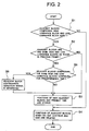
- the high/low luminance adjacent block detecting circuit 14 discriminates for each frame whether the adjacent blocks (block pair), which consist of a high luminance block and a low luminance block, exist or not in the detected high luminance block (blocks) and low luminance block (blocks) (step S1), as shown in Fig. 2. If the adjacent blocks in which the high luminance block and the low luminance block are neighboring mutually exist, whether the adjacent blocks have already been detected as adjacent blocks consisting of the same high luminance block and low luminance block in the previous frame or not is discriminated (step S2).
- step S3 If the present detected adjacent blocks are not the adjacent blocks consisting of the same high luminance block and low luminance block in the previous frame, the positions of the adjacent blocks and the present time are stored into an internal memory (not shown) (step S3). After completion of the execution in step S3, the positions of the adjacent blocks which do not continue in the previous and present frames and the stored time are deleted from the internal memory (step S4). Step S4 is also executed in the case where the adjacent blocks consisting of a high luminance block and a low luminance block do not exist in the present frame.
- step S5 If it is determined in step S2 that the adjacent blocks in the present frame has already continued the state of the same high luminance block and low luminance block in the previous frame, whether the state of the same high luminance block and low luminance block has continued for a predetermined time or not is discriminated (step S5).
- the continuation time is discriminated from the time stored in the internal memory.
- the predetermined time is set to, for example, a few seconds. If the adjacent blocks have continued the state of the same high luminance block and low luminance block for the predetermined time, the adjacent block continuation detection signal is generated to the control circuit 3 (step S6).
- step S3 follows. Also after completion of the execution in step S6, the processing routine advances to step S3.
- the adjacent block continuation detection signal is generated from the high/low luminance adjacent block detecting circuit 14.
- the control circuit 3 issues a level restriction command to the level adjusting circuit 2 in response to the adjacent block continuation detection signal.
- the level adjusting circuit 2 restricts the luminance level of the supplied pixel data D.
- the restricted pixel data D is supplied to the frame memory device 4.
- the pixel data D is sequentially supplied to the address driver 6.
- the PDP 10 is driven by the address driver 6, first sustain driver 7, and second sustain driver 8, so that an image corresponding to the input image signal is displayed by the PDP 10.
- the display by the PDP 10 if the luminance level of the pixel data D is restricted by the level adjusting circuit 2, the large temperature difference is suppressed in the boundary portion of the high luminance block and the low luminance block, so that the deterioration of the display panel of the PDP 10 can be prevented.
- the display period of time of one field is divided into N subfields, the number of light emitting times corresponding to the weight of the bit digit of the pixel data (N bits) according to the input image signal is allocated every subfield, and the light emission driving is performed.
- the number of light emitting times of each subfield can be also reduced in response to the adjacent block continuation detection signal.
- the embodiment has been described with respect to the example in which the invention is applied to the display apparatus using the PDP, the invention is not limited to it but can be also applied to another display apparatus using a display panel with an organic EL device.
- the luminance level does not decrease unnecessarily and a situation that the frame is darkened due to the luminance restriction as in the conventional apparatus can be prevented.
Abstract
Description
Claims (3)
- A display apparatus comprising:average luminance level detecting means for dividing a frame shown by an input image signal into a plurality of blocks and detecting an average luminance level of said image signal in each of the plurality of blocks;adjacent block detecting means for detecting adjacent blocks having a relation such that a difference of the average luminance levels is equal to or larger than a predetermined level from the plurality of blocks in accordance with the average luminance level of each of the plurality of blocks detected by said average luminance level detecting means;state continuation detecting means for detecting that the adjacent blocks detected by said adjacent block detecting means have continued the state where the difference of the average luminance levels is equal to or larger than the predetermined level for a predetermined time, to generate a luminance restriction command signal; anddisplay means for displaying an image corresponding to said image signal while restricting a luminance level of said image signal in response to said luminance restriction command signal.
- An apparatus according to claim 1, wherein said adjacent block detecting means includes:high luminance block detecting means for comparing the average luminance level of each of said plurality of blocks detected by said average luminance level detecting means with a first reference value, thereby detecting a block whose average luminance level is equal to or larger than said first reference value;low luminance block detecting means for comparing the average luminance level of each of said plurality of blocks detected by said average luminance level detecting means with a second reference value, thereby detecting a block whose average luminance level is equal to or smaller than said second reference value; andmeans for detecting a block pair in which the block detected by said high luminance block detecting means and the block detected by said low luminance block detecting means are neighboring mutually as the adjacent blocks.
- A displaying method comprising the steps of:dividing a frame shown by an input image signal into a plurality of blocks and detecting an average luminance level of said image signal in each of the plurality of block;detecting adjacent blocks having a relation such that a difference of the average luminance levels is equal to or larger than a predetermined level from the plurality of blocks in accordance with the average luminance level of each of the plurality of blocks;detecting that the adjacent blocks have continued the state where the difference of the average luminance levels is equal to or larger than the predetermined level for a predetermined time, to generate a luminance restriction command signal; anddisplaying an image corresponding to said image signal while restricting a luminance level of said image signal in response to said luminance restriction command signal.
Applications Claiming Priority (2)
| Application Number | Priority Date | Filing Date | Title |
|---|---|---|---|
| JP2001174062A JP4610793B2 (en) | 2001-06-08 | 2001-06-08 | Display apparatus and method |
| JP2001174062 | 2001-06-08 |
Publications (2)
| Publication Number | Publication Date |
|---|---|
| EP1265213A2 true EP1265213A2 (en) | 2002-12-11 |
| EP1265213A3 EP1265213A3 (en) | 2005-04-20 |
Family
ID=19015403
Family Applications (1)
| Application Number | Title | Priority Date | Filing Date |
|---|---|---|---|
| EP02010878A Withdrawn EP1265213A3 (en) | 2001-06-08 | 2002-05-15 | Display apparatus and display method |
Country Status (3)
| Country | Link |
|---|---|
| US (1) | US6617797B2 (en) |
| EP (1) | EP1265213A3 (en) |
| JP (1) | JP4610793B2 (en) |
Cited By (5)
| Publication number | Priority date | Publication date | Assignee | Title |
|---|---|---|---|---|
| EP1475769A2 (en) * | 2003-05-07 | 2004-11-10 | Grundig Multimedia B.V. | Method and device for improving the grey scale resolution of a pulse width modulated image display device |
| EP1591990A1 (en) | 2004-04-27 | 2005-11-02 | Pioneer Corporation | Display device drive apparatus and drive method |
| EP1603104A2 (en) * | 2004-06-03 | 2005-12-07 | LG Electronics Inc. | Plasma display apparatus and driving method of the same |
| EP1612831A2 (en) * | 2004-07-02 | 2006-01-04 | LG Electronics Inc. | Plasma display apparatus and driving method thereof |
| CN100347735C (en) * | 2002-12-27 | 2007-11-07 | 夏普株式会社 | Method for driving displaying device, displaying device and related computer programm |
Families Citing this family (12)
| Publication number | Priority date | Publication date | Assignee | Title |
|---|---|---|---|---|
| JP3995505B2 (en) * | 2002-03-25 | 2007-10-24 | 三洋電機株式会社 | Display method and display device |
| US8502762B2 (en) * | 2003-03-31 | 2013-08-06 | Sharp Kabushiki Kaisha | Image processing method and liquid-crystal display device using the same |
| US20050200291A1 (en) * | 2004-02-24 | 2005-09-15 | Naugler W. E.Jr. | Method and device for reading display pixel emission and ambient luminance levels |
| KR20050112251A (en) * | 2004-05-25 | 2005-11-30 | 삼성전자주식회사 | Display apparatus and control method thereof |
| JP5137325B2 (en) * | 2006-04-27 | 2013-02-06 | 株式会社日立製作所 | Plasma display device and processing method thereof |
| KR101279117B1 (en) * | 2006-06-30 | 2013-06-26 | 엘지디스플레이 주식회사 | OLED display and drive method thereof |
| KR100856411B1 (en) * | 2006-12-01 | 2008-09-04 | 삼성전자주식회사 | Method and apparatus for compensating illumination compensation and method and apparatus for encoding moving picture based on illumination compensation, and method and apparatus for encoding moving picture based on illumination compensation |
| KR100833758B1 (en) * | 2007-01-15 | 2008-05-29 | 삼성에스디아이 주식회사 | Organic light emitting display and image modification method |
| WO2009157224A1 (en) * | 2008-06-27 | 2009-12-30 | シャープ株式会社 | Control device of liquid crystal display device, liquid crystal display device, method for controlling liquid crystal display device, program, and recording medium |
| JP5304211B2 (en) * | 2008-12-11 | 2013-10-02 | ソニー株式会社 | Display device, brightness adjusting device, backlight device, brightness adjusting method and program |
| KR20100131232A (en) * | 2009-06-05 | 2010-12-15 | 삼성모바일디스플레이주식회사 | Display and driving method thereof |
| KR20230065423A (en) * | 2021-11-04 | 2023-05-12 | 삼성디스플레이 주식회사 | Display device |
Citations (2)
| Publication number | Priority date | Publication date | Assignee | Title |
|---|---|---|---|---|
| EP0888004A2 (en) * | 1997-06-27 | 1998-12-30 | Pioneer Electronic Corporation | Brightness controlling apparatus |
| EP0973331A1 (en) * | 1998-07-17 | 2000-01-19 | Deutsche Thomson-Brandt Gmbh | Arrangement for regulating the luminance |
Family Cites Families (7)
| Publication number | Priority date | Publication date | Assignee | Title |
|---|---|---|---|---|
| JP3455265B2 (en) * | 1994-01-25 | 2003-10-14 | パイオニア株式会社 | Driving circuit and driving method for flat display device |
| JP3345184B2 (en) * | 1994-09-07 | 2002-11-18 | パイオニア株式会社 | Multi-scan adaptive plasma display device and driving method thereof |
| JP3045284B2 (en) * | 1997-10-16 | 2000-05-29 | 日本電気株式会社 | Moving image display method and device |
| JP3642170B2 (en) * | 1998-02-02 | 2005-04-27 | 三菱電機株式会社 | Plasma display panel temperature control method and plasma display apparatus |
| JP4016493B2 (en) * | 1998-08-05 | 2007-12-05 | 三菱電機株式会社 | Display device and multi-gradation circuit thereof |
| JP3695737B2 (en) * | 1999-07-01 | 2005-09-14 | パイオニア株式会社 | Driving device for plasma display panel |
| US6396508B1 (en) * | 1999-12-02 | 2002-05-28 | Matsushita Electronics Corp. | Dynamic low-level enhancement and reduction of moving picture disturbance for a digital display |
-
2001
- 2001-06-08 JP JP2001174062A patent/JP4610793B2/en not_active Expired - Fee Related
-
2002
- 2002-05-15 EP EP02010878A patent/EP1265213A3/en not_active Withdrawn
- 2002-05-21 US US10/150,970 patent/US6617797B2/en not_active Expired - Fee Related
Patent Citations (2)
| Publication number | Priority date | Publication date | Assignee | Title |
|---|---|---|---|---|
| EP0888004A2 (en) * | 1997-06-27 | 1998-12-30 | Pioneer Electronic Corporation | Brightness controlling apparatus |
| EP0973331A1 (en) * | 1998-07-17 | 2000-01-19 | Deutsche Thomson-Brandt Gmbh | Arrangement for regulating the luminance |
Non-Patent Citations (2)
| Title |
|---|
| PATENT ABSTRACTS OF JAPAN vol. 1995, no. 11, 26 December 1995 (1995-12-26) -& JP 07 210109 A (PIONEER ELECTRON CORP), 11 August 1995 (1995-08-11) * |
| PATENT ABSTRACTS OF JAPAN vol. 1999, no. 13, 30 November 1999 (1999-11-30) -& JP 11 219152 A (MITSUBISHI ELECTRIC CORP), 10 August 1999 (1999-08-10) * |
Cited By (8)
| Publication number | Priority date | Publication date | Assignee | Title |
|---|---|---|---|---|
| CN100347735C (en) * | 2002-12-27 | 2007-11-07 | 夏普株式会社 | Method for driving displaying device, displaying device and related computer programm |
| EP1475769A2 (en) * | 2003-05-07 | 2004-11-10 | Grundig Multimedia B.V. | Method and device for improving the grey scale resolution of a pulse width modulated image display device |
| EP1475769A3 (en) * | 2003-05-07 | 2009-07-15 | Grundig Multimedia B.V. | Method and device for improving the grey scale resolution of a pulse width modulated image display device |
| EP1591990A1 (en) | 2004-04-27 | 2005-11-02 | Pioneer Corporation | Display device drive apparatus and drive method |
| EP1603104A2 (en) * | 2004-06-03 | 2005-12-07 | LG Electronics Inc. | Plasma display apparatus and driving method of the same |
| EP1603104A3 (en) * | 2004-06-03 | 2006-08-23 | LG Electronics Inc. | Plasma display apparatus and driving method of the same |
| EP1612831A2 (en) * | 2004-07-02 | 2006-01-04 | LG Electronics Inc. | Plasma display apparatus and driving method thereof |
| EP1612831A3 (en) * | 2004-07-02 | 2007-06-06 | LG Electronics Inc. | Plasma display apparatus and driving method thereof |
Also Published As
| Publication number | Publication date |
|---|---|
| JP4610793B2 (en) | 2011-01-12 |
| EP1265213A3 (en) | 2005-04-20 |
| JP2002366087A (en) | 2002-12-20 |
| US6617797B2 (en) | 2003-09-09 |
| US20020195957A1 (en) | 2002-12-26 |
Similar Documents
| Publication | Publication Date | Title |
|---|---|---|
| US6617797B2 (en) | Display apparatus and display method | |
| US6465970B2 (en) | Plasma display panel driving method | |
| US6278422B1 (en) | Method of driving plasma display panel and display apparatus | |
| US7233300B2 (en) | Apparatus and method for displaying gray scales of plasma display panel | |
| US7142175B2 (en) | Method and apparatus for displaying grayscale of plasma display panel | |
| KR20010098797A (en) | Cascade stage plasma display panel for reducing the power in writing the data | |
| US7525513B2 (en) | Method and apparatus for driving plasma display panel having operation mode selection based on motion detected | |
| US6798393B2 (en) | Plasma display device | |
| KR100603311B1 (en) | Panel driving method and apparatus | |
| US6753831B1 (en) | Display device | |
| JP2002023694A (en) | Multigradation image display device which reduces power consumption during data writing | |
| JPH10319900A (en) | Driving method of plasma display device | |
| US6999047B1 (en) | Displaying video on a plasma display panel | |
| US20100026675A1 (en) | Driving method of plasma display device | |
| KR100271132B1 (en) | Apparatus for protesting screen and driving thereof for plasma display panel | |
| KR20060001406A (en) | Driving method of plasma display panel | |
| US20070109222A1 (en) | Plasma display device and driving method thereof | |
| KR100542212B1 (en) | Driving method of plasma display panel and apparatus thereof | |
| KR100489277B1 (en) | Method and apparatus for driving plasma display panel | |
| KR100560500B1 (en) | Driving device of plasma display panel and driving method thereof | |
| KR100573136B1 (en) | Method and apparatus for driving display panel | |
| KR100257484B1 (en) | Plasma display panel and its control method | |
| JP2003066893A (en) | Driving method for plasma display panel | |
| KR100581878B1 (en) | Driving method and apparatus of plasma display panel | |
| KR100490627B1 (en) | Method and device for driving of plasma display panel |
Legal Events
| Date | Code | Title | Description |
|---|---|---|---|
| PUAI | Public reference made under article 153(3) epc to a published international application that has entered the european phase |
Free format text: ORIGINAL CODE: 0009012 |
|
| AK | Designated contracting states |
Kind code of ref document: A2 Designated state(s): AT BE CH CY DE DK ES FI FR GB GR IE IT LI LU MC NL PT SE TR |
|
| AX | Request for extension of the european patent |
Free format text: AL;LT;LV;MK;RO;SI |
|
| RAP1 | Party data changed (applicant data changed or rights of an application transferred) |
Owner name: PIONEER DISPLAY PRODUCTS CORPORATION Owner name: PIONEER CORPORATION |
|
| PUAL | Search report despatched |
Free format text: ORIGINAL CODE: 0009013 |
|
| AK | Designated contracting states |
Kind code of ref document: A3 Designated state(s): AT BE CH CY DE DK ES FI FR GB GR IE IT LI LU MC NL PT SE TR |
|
| AX | Request for extension of the european patent |
Extension state: AL LT LV MK RO SI |
|
| 17P | Request for examination filed |
Effective date: 20050413 |
|
| AKX | Designation fees paid |
Designated state(s): DE FR GB |
|
| GRAP | Despatch of communication of intention to grant a patent |
Free format text: ORIGINAL CODE: EPIDOSNIGR1 |
|
| STAA | Information on the status of an ep patent application or granted ep patent |
Free format text: STATUS: THE APPLICATION IS DEEMED TO BE WITHDRAWN |
|
| 18D | Application deemed to be withdrawn |
Effective date: 20080829 |