JP4016493B2 - Display device and multi-gradation circuit thereof - Google Patents
Display device and multi-gradation circuit thereof Download PDFInfo
- Publication number
- JP4016493B2 JP4016493B2 JP22199998A JP22199998A JP4016493B2 JP 4016493 B2 JP4016493 B2 JP 4016493B2 JP 22199998 A JP22199998 A JP 22199998A JP 22199998 A JP22199998 A JP 22199998A JP 4016493 B2 JP4016493 B2 JP 4016493B2
- Authority
- JP
- Japan
- Prior art keywords
- video signal
- dither
- average value
- signal
- pixels
- Prior art date
- Legal status (The legal status is an assumption and is not a legal conclusion. Google has not performed a legal analysis and makes no representation as to the accuracy of the status listed.)
- Expired - Fee Related
Links
Images

Classifications
-
- G—PHYSICS
- G09—EDUCATION; CRYPTOGRAPHY; DISPLAY; ADVERTISING; SEALS
- G09G—ARRANGEMENTS OR CIRCUITS FOR CONTROL OF INDICATING DEVICES USING STATIC MEANS TO PRESENT VARIABLE INFORMATION
- G09G3/00—Control arrangements or circuits, of interest only in connection with visual indicators other than cathode-ray tubes
- G09G3/20—Control arrangements or circuits, of interest only in connection with visual indicators other than cathode-ray tubes for presentation of an assembly of a number of characters, e.g. a page, by composing the assembly by combination of individual elements arranged in a matrix no fixed position being assigned to or needed to be assigned to the individual characters or partial characters
- G09G3/2007—Display of intermediate tones
- G09G3/2044—Display of intermediate tones using dithering
- G09G3/2051—Display of intermediate tones using dithering with use of a spatial dither pattern
- G09G3/2055—Display of intermediate tones using dithering with use of a spatial dither pattern the pattern being varied in time
-
- G—PHYSICS
- G09—EDUCATION; CRYPTOGRAPHY; DISPLAY; ADVERTISING; SEALS
- G09G—ARRANGEMENTS OR CIRCUITS FOR CONTROL OF INDICATING DEVICES USING STATIC MEANS TO PRESENT VARIABLE INFORMATION
- G09G3/00—Control arrangements or circuits, of interest only in connection with visual indicators other than cathode-ray tubes
- G09G3/20—Control arrangements or circuits, of interest only in connection with visual indicators other than cathode-ray tubes for presentation of an assembly of a number of characters, e.g. a page, by composing the assembly by combination of individual elements arranged in a matrix no fixed position being assigned to or needed to be assigned to the individual characters or partial characters
- G09G3/2007—Display of intermediate tones
- G09G3/2077—Display of intermediate tones by a combination of two or more gradation control methods
-
- G—PHYSICS
- G09—EDUCATION; CRYPTOGRAPHY; DISPLAY; ADVERTISING; SEALS
- G09G—ARRANGEMENTS OR CIRCUITS FOR CONTROL OF INDICATING DEVICES USING STATIC MEANS TO PRESENT VARIABLE INFORMATION
- G09G3/00—Control arrangements or circuits, of interest only in connection with visual indicators other than cathode-ray tubes
- G09G3/20—Control arrangements or circuits, of interest only in connection with visual indicators other than cathode-ray tubes for presentation of an assembly of a number of characters, e.g. a page, by composing the assembly by combination of individual elements arranged in a matrix no fixed position being assigned to or needed to be assigned to the individual characters or partial characters
- G09G3/2092—Details of a display terminals using a flat panel, the details relating to the control arrangement of the display terminal and to the interfaces thereto
-
- G—PHYSICS
- G09—EDUCATION; CRYPTOGRAPHY; DISPLAY; ADVERTISING; SEALS
- G09G—ARRANGEMENTS OR CIRCUITS FOR CONTROL OF INDICATING DEVICES USING STATIC MEANS TO PRESENT VARIABLE INFORMATION
- G09G2320/00—Control of display operating conditions
- G09G2320/02—Improving the quality of display appearance
- G09G2320/0261—Improving the quality of display appearance in the context of movement of objects on the screen or movement of the observer relative to the screen
-
- G—PHYSICS
- G09—EDUCATION; CRYPTOGRAPHY; DISPLAY; ADVERTISING; SEALS
- G09G—ARRANGEMENTS OR CIRCUITS FOR CONTROL OF INDICATING DEVICES USING STATIC MEANS TO PRESENT VARIABLE INFORMATION
- G09G2320/00—Control of display operating conditions
- G09G2320/02—Improving the quality of display appearance
- G09G2320/0271—Adjustment of the gradation levels within the range of the gradation scale, e.g. by redistribution or clipping
- G09G2320/0276—Adjustment of the gradation levels within the range of the gradation scale, e.g. by redistribution or clipping for the purpose of adaptation to the characteristics of a display device, i.e. gamma correction
-
- G—PHYSICS
- G09—EDUCATION; CRYPTOGRAPHY; DISPLAY; ADVERTISING; SEALS
- G09G—ARRANGEMENTS OR CIRCUITS FOR CONTROL OF INDICATING DEVICES USING STATIC MEANS TO PRESENT VARIABLE INFORMATION
- G09G3/00—Control arrangements or circuits, of interest only in connection with visual indicators other than cathode-ray tubes
- G09G3/20—Control arrangements or circuits, of interest only in connection with visual indicators other than cathode-ray tubes for presentation of an assembly of a number of characters, e.g. a page, by composing the assembly by combination of individual elements arranged in a matrix no fixed position being assigned to or needed to be assigned to the individual characters or partial characters
- G09G3/2007—Display of intermediate tones
- G09G3/2018—Display of intermediate tones by time modulation using two or more time intervals
- G09G3/2022—Display of intermediate tones by time modulation using two or more time intervals using sub-frames
-
- G—PHYSICS
- G09—EDUCATION; CRYPTOGRAPHY; DISPLAY; ADVERTISING; SEALS
- G09G—ARRANGEMENTS OR CIRCUITS FOR CONTROL OF INDICATING DEVICES USING STATIC MEANS TO PRESENT VARIABLE INFORMATION
- G09G3/00—Control arrangements or circuits, of interest only in connection with visual indicators other than cathode-ray tubes
- G09G3/20—Control arrangements or circuits, of interest only in connection with visual indicators other than cathode-ray tubes for presentation of an assembly of a number of characters, e.g. a page, by composing the assembly by combination of individual elements arranged in a matrix no fixed position being assigned to or needed to be assigned to the individual characters or partial characters
- G09G3/22—Control arrangements or circuits, of interest only in connection with visual indicators other than cathode-ray tubes for presentation of an assembly of a number of characters, e.g. a page, by composing the assembly by combination of individual elements arranged in a matrix no fixed position being assigned to or needed to be assigned to the individual characters or partial characters using controlled light sources
- G09G3/28—Control arrangements or circuits, of interest only in connection with visual indicators other than cathode-ray tubes for presentation of an assembly of a number of characters, e.g. a page, by composing the assembly by combination of individual elements arranged in a matrix no fixed position being assigned to or needed to be assigned to the individual characters or partial characters using controlled light sources using luminous gas-discharge panels, e.g. plasma panels
- G09G3/2803—Display of gradations
Landscapes
- Engineering & Computer Science (AREA)
- Physics & Mathematics (AREA)
- Computer Hardware Design (AREA)
- General Physics & Mathematics (AREA)
- Theoretical Computer Science (AREA)
- Control Of Indicators Other Than Cathode Ray Tubes (AREA)
- Image Processing (AREA)
- Transforming Electric Information Into Light Information (AREA)
Description
【0001】
【発明の属する技術分野】
この発明は、ディザ信号処理によってディスプレイ装置の階調表現能力を高める多階調化回路、及び当該多階調化回路を備えたディスプレイ装置に関し、特に多階調化が困難なプラズマディスプレイやディジタルマクロミラーデバイスなどに用いる多階調化回路に関する。
【0002】
【従来の技術】
明るさが様々に変化する画像を表示するためには、ディスプレイ装置には階調表現ができることが必要である。
【0003】
プラズマディスプレイ装置では、1フィールドの期間を複数のサブフィールドに分割し、画面上の各画素が各サブフィールドにおいて発光を行うか否かを、ディスプレイ装置に入力される映像信号に応じて選択することによって階調表現を行っている。
【0004】
図26に1フィールドAFを8つのサブフィールドSF0からSF7に分割して構成した表示シーケンスの例を示す。各サブフィールドSFにおける発光時間の相対比は、1:2:4:8:16:32:64:128になっており、これらの発光、非発光の組み合わせにより256(1+2+4+8+16+32+64+128)の階調を表現する能力がある。
【0005】
例えば、ある画素において127(1+2+4+8+16+32+64)という階調を表現する場合には、サブフィールドSF0からSF6において発光を行い、サブフィールドSF7においては発光を行わないとする。人間の視覚は1フィールドAF内の発光の明滅には応答しないため、サブフィールドSF0からSF6までの発光が時間方向に積分され、人間の目にはあたかも127という階調が表現されているように知覚される。
【0006】
このディスプレイ装置に映像信号を表示する場合には、映像信号を最終的に8ビットのディジタル信号に変換し、最下位ビットb0をサブフィールドSF0に、その1つ上位のビットb1をサブフィールドSF1に、さらにその1つ上位のビットb2をサブフィールドSF2に、以下同様にしてビットb2よりも1つ上位のビットb3から最上位ビットb7までをそれぞれサブフィールドSF3からSF7に割り当て、1という値が設定されたビットに対応するサブフィールドにおいては発光を行うようにし、0という値が設定されたビットに対応するサブフィールドにおいては発光を行わないようにする。例えば、2進表記で(01111111)という8ビットのディジタル映像信号を表示に用いる場合は、最下位ビットb0からビットb6までに1が設定され、最上位ビットb7には0が設定されているので、サブフィールドSF0からSF6において発光が行われ、サブフィールドSF7では発光は行われないことになる。なお、図26において、AD0からAD7は各サブフィールドSF0からSF7におけるアドレス期間、CF0からCF7は同じく維持放電期間であり、詳細は後述する。
【0007】
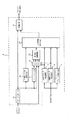
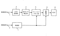
図27は従来のディスプレイ装置の階調表現方法を実現する構成例であり、1は映像信号を入力する入力端子、2は同期信号を入力する入力端子、3は入力端子1に入力された映像信号を、ディジタル信号に変換するA/D変換部、4は放送局でガンマ補正された映像信号を逆変換し、放送局で撮影された明るさを後述するPDP8(以下同様にプラズマディスプレイパネルをPDPと略記する)で再現できるようにする逆ガンマ補正部、5は逆ガンマ補正部4の出力信号を2フィールド分記憶するフィールドメモリ部、6はフィールドメモリ部5及び後述する制御部7の出力信号によりPDP8を駆動する駆動部、7は同期信号を基準として、フィールドメモリ部5、及び駆動部6を制御する制御部、8はPDPである。
【0008】
以下、上述のように構成されたディスプレイ装置の動作について説明する。
【0009】
入力端子1より入力された映像信号は、A/D変換部3で8ビットのディジタル信号に変換され、逆ガンマ補正部4においてガンマ補正の逆関数による映像信号レベルの補正が行われる。逆ガンマ補正部4から出力される8ビットの映像信号はフィールドメモリ部5で2フィールド分記憶される。フィールドメモリ部5は1フィールド分の映像信号を記憶することができる2つのフィールドメモリを持っており、入力された映像信号は、図26に示した1フィールドAF毎に異なるフィールドメモリに対して交互に書き込まれる。
【0010】
次に図26に示すサブフィールドSF0のアドレス期間AD0において、図27に示したフィールドメモリ部5から画面上のすべての画素に関して映像信号の最下位ビットのデータであるb0が読み出される。この読み出し動作は制御部7によって書き込み動作が行われていない方のフィールドメモリに対して行われるように制御される。読み出されたデータは駆動部6を通してPDP8に書き込まれる。AC型PDPの場合には、パネルにメモリ効果があるため、書き込まれたデータは、画面上のすべての画素に対して書き込み動作が行われる間中保持されている。図26に示したサブフィールドSF0のアドレス期間AD0に続く維持放電期間CF0に、図27に示した制御部7が駆動部6を制御することで、1のデータが書き込まれた画素のみPDP8は発光を行う。
【0011】
次の図26に示したサブフィールドSF1のアドレス期間AD1には、ビットb1のデータが図27に示したフィールドメモリ部5から読み出され、駆動部6を経由してPDP8に供給される。図26に示したサブフィールドSF1の維持放電期間CF1には1のデータが書き込まれた画素が、維持放電期間CF0における発光時間の2倍の時間の発光を行う。
【0012】
以下、サブフィールドSF2からSF7においても同様に、対応するビットb2からb7までの各データが各アドレス期間AD2からAD7において図27のフィールドメモリ部5から読み出され、駆動部6を経由してPDP8に供給され、1のデータが書き込まれた画素は各維持放電期間CF2からCF7に維持放電期間CF0における発光時間のそれぞれ4倍、8倍、16倍、32倍、64倍、128倍の時間の発光を行う。
【0013】
【発明が解決しようとする課題】
以上のような構成で階調表現を行うディスプレイ装置では、多階調化が時間的な制約により困難である。このようなディスプレイ装置で単純に多階調化を実現するにはサブフィールド数を増やせばよい。例えば図26に示した1フィールドAFを10個のサブフィールドに分割し、各サブフィールドの発光時間の相対比を1:2:4:8:16:32:64:128:256:512とすれば1024の階調を表現することが可能である(前述したように8個のサブフィールドSF0からSF7を用いた場合は256階調)。
【0014】
しかし、各サブフィールド(例えば、SF0からSF7)には、画面上のすべての画素に関してデータを書き込むために一定のアドレス期間(例えば、AD0からAD7)が必要であり、1フィールドAFという制限された期間内においてより多くのサブフィールドを用いて図27に示したPDP8を駆動しようとすると、アドレス期間の総和はサブフィールド数に比例して長くなる分、維持放電期間の総和はより短くなるため、ディスプレイ装置の全体的な発光輝度が低下してしまう。このためディスプレイ装置の発光輝度を十分なレベルに保ちつつ、同時に階調表現能力を高めることが困難であるという問題があった。
【0015】
また、このようなディスプレイ装置において例えば図26のような表示シーケンスで階調表現を行う場合、画素にデータをまったく書き込まない場合に表現される階調である階調0を除外して考えると、サブフィールドSF0のみにデータ1を書き込む場合の階調1が最低の階調であり、このディスプレイ装置で表現可能なすべての階調は、階調1の整数倍の明るさとなっている。
【0016】
一方で人間の視覚は暗部側で特に階調識別能力が高いため、ディスプレイ装置は特に低階調側においてより微妙な階調の差異を表現する必要がある。しかし、従来のディスプレイ装置では前述したように表現可能なすべての階調は階調1の整数倍であるから、明部においても暗部においても互いに隣接する階調間の明るさの差異は一定となり、明部では十分な階調表現能力があっても、暗部での階調表現能力が不十分になりやすく、結果的に階調が滑らかに変化する暗い画像を表示しようとすると階調の粗い不自然な画像として知覚されてしまうという問題があった。
【0017】
この発明は、ディスプレイ装置において優れた階調表現を行うための多階調化回路を提供すること、暗部側で優れた階調表現を行うための多階調化回路を提供すること、及び当該多階調化回路を備えたディスプレイ装置を提供することを目的とする。
【0018】
【課題を解決するための手段】
この発明に係るディスプレイ装置の多階調化回路は、m+n(m、nは1以上の整数)ビットのディジタル映像信号をmビットのディジタル映像信号に変換する処理を有するディスプレイ装置の多階調化回路において、ディスプレイ画面上を複数の領域に分割し、この領域内における画素の相対的な空間座標を特定する空間座標特定手段と、画素の、所定の周期内における相対的な時間座標を特定する時間座標特定手段と、空間座標特定手段及び時間座標特定手段が特定する画素を含む複数の画素に関するm+nビットのディジタル映像信号について、下位nビットのうちの少なくとも上位1ビット以上を用いて所定の平均値又は総和を演算する平均値演算手段と、少なくとも空間座標特定手段が画素について特定した空間座標、時間座標特定手段が画素について特定した時間座標、及び平均値演算手段の演算結果に基づいてディザ信号を与えるディザ信号発生手段と、空間座標特定手段が画素について特定した空間座標に存在する画素に関するディジタル映像信号に対して、ディザ信号発生手段によって与えられたディザ信号を加減算する加減算手段とを備えたものである。
【0019】
また、この発明に係るディスプレイ装置の多階調化回路は、領域を1つ以上の部分領域に分割し、平均値演算手段は、空間座標特定手段及び時間座標特定手段が特定する画素を含む部分領域内の複数の画素に関するm+nビットのディジタル映像信号について、下位nビットのうちの少なくとも上位1ビット以上を用いて所定の平均値または総和を求め、ディザ信号発生手段は、変換前のディジタル映像信号の部分領域内の平均レベルと、変換後のディジタル映像信号の部分領域内の平均レベルとが、m+nビットに換算して略等しくなるようなディザ信号の与え方を有するものである。
【0020】
また、この発明に係るディスプレイ装置の多階調化回路は、領域を1つ以上の部分領域に分割し、さらに部分領域を2つ以上の単位領域に分割し、平均値演算手段は、空間座標特定手段及び時間座標特定手段が特定する画素を含む単位領域内の複数の画素に関するm+nビットのディジタル映像信号について、下位nビットのうちの少なくとも上位1ビット以上を用いて所定の平均値または総和を求め、ディザ信号発生手段は、平均値演算手段の演算結果が、1つの部分領域を構成する各単位領域どうしにおいて略等しい場合には、変換前のディジタル映像信号の部分領域内の平均レベルと、変換後のディジタル映像信号の部分領域内の平均レベルとが、m+nビットに換算して略等しくなるようなディザ信号の与え方を有するものである。
【0021】
また、この発明に係るディスプレイ装置の多階調化回路は、領域を1つ以上の部分領域に分割し、さらに部分領域を2つ以上の単位領域に分割し、平均値演算手段は、空間座標特定手段及び時間座標特定手段が特定する画素を含む単位領域内の複数の画素に関するm+nビットのディジタル映像信号について、下位nビットのうちの少なくとも上位1ビット以上を用いて所定の平均値または総和を求め、ディザ信号発生手段は、平均値演算手段の演算結果が、連続するf(fは2以上の整数)個の時間座標にわたって、1つの部分領域を構成する各単位領域どうしにおいて略等しい場合には、変換前のディジタル映像信号の、部分領域内の連続するf個の時間座標にわたる平均レベルと、変換後のディジタル映像信号の、部分領域内の連続するf個の時間座標にわたる平均レベルとが、m+nビットに換算して略等しくなるようなディザ信号の与え方を有するものである。
【0022】
また、この発明に係るディスプレイ装置の多階調化回路は、空間座標特定手段が特定した空間座標、時間座標特定手段が特定した時間座標、平均値演算手段の演算結果、及び外部より入力されたディザパターン選択信号に基づいてディザ信号を与えるディザ信号発生手段を備え、ディザ信号発生手段は、空間座標特定手段が特定した空間座標、時間座標特定手段が特定した時間座標、及び平均値演算手段の演算結果が同じであるときでも異なる複数のディザ信号の与え方を有する場合には、ディザパターン選択信号により、異なる複数のディザ信号の与え方の中から1つの与え方を選択するものである。
【0023】
また、この発明に係るディスプレイ装置の多階調化回路は、ディジタル映像信号を1つ以上の閾値と比較する比較手段と、空間座標特定手段が特定した空間座標、時間座標特定手段が特定した時間座標、平均値演算手段の演算結果、及び比較手段の比較結果に基づいてディザ信号を与えるディザ信号発生手段を備え、ディザ信号発生手段は、空間座標特定手段が特定した空間座標、時間座標特定手段が特定した時間座標、及び平均値演算手段の演算結果が同じであるときでも異なる複数のディザ信号の与え方を有する場合には、比較手段の比較結果により、異なる複数のディザ信号の与え方の中から1つの与え方を選択するものである。
【0024】
また、この発明に係るディスプレイ装置の多階調化回路は、平均値演算手段は、空間座標特定手段が特定した空間座標に存在する画素と、この画素に関するディジタル映像信号に対して信号レベルの差異がある閾値以下であるディジタル映像信号をもつ画素とに関して、m+nビットのディジタル映像信号の下位nビットのうちの少なくとも上位1ビット以上を用いて所定の平均値又は総和を演算するものである。
【0025】
また、この発明に係るディスプレイ装置の多階調化回路は、ディジタル映像信号を1つ以上の閾値と比較する比較手段と、ディジタル映像信号の下位ビットの値を固定し、値を固定するビット長を比較手段の比較結果に応じて変化させるビットマスク手段を備えたものである。
【0026】
さらにまた、この発明に係るディスプレイ装置は、映像信号をm+nビットのディジタル映像信号に変換するA/D変換部と、m+nビットのディジタル映像信号に対してディザ信号を加減算する前述のディスプレイ装置の多階調化回路と、ディザ信号が加算されたm+nビットのディジタル映像信号の上位mビットを表示する画素とを備えたものである。
【0027】
【発明の実施の形態】
実施の形態1.
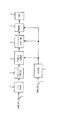
図1はこの発明の実施の形態1に関わるディスプレイ装置の全体構成を示すブロック図であり、ディスプレイ装置の多階調化を実現するものである。なお、実施の形態1であるディスプレイ装置の多階調化回路を説明するにあたり、前記図27に示すディスプレイ装置と同一構成部分には同一符号を付している。
【0028】
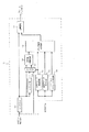
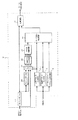
図1において、1は映像信号を入力する入力端子、2は同期信号を入力する入力端子、3は入力端子1に入力された映像信号を、ディジタル信号に変換するA/D変換部、4は放送局でガンマ補正された映像信号を逆変換し、放送局で撮影された明るさをPDP8で再現できるようにする逆ガンマ補正部、9は逆ガンマ補正部4の出力信号に対して、ディザ信号を加算する多階調化処理部、5は多階調化処理部9の出力信号を、2フィールド分記憶するフィールドメモリ部、6はフィールドメモリ部5及び後述する制御部7の出力信号によりPDP8を駆動する駆動部、7は同期信号を基準として、多階調化処理部9、フィールドメモリ部5、及び駆動部6を制御する制御部、8はPDPである。ここで逆ガンマ補正部4の出力端においては、ディスプレイで表示可能な階調数を表現するために必要なビット数よりも多いビット数を持つディジタル信号となっている。
【0029】
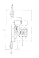
ここでさらに、多階調化処理部9について、その構成の詳細を図2に示す。
【0030】
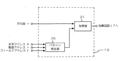
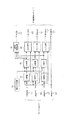
図において、10は逆ガンマ補正部4から出力されたディジタル信号を1ライン分記憶しておくラインメモリA、11はラインメモリA10から出力されたディジタル映像信号のうちディスプレイで表示できる最も低い映像信号レベルよりも低いレベルの映像信号成分(これを以下「非表示となる映像信号成分」と呼ぶ)を1ライン分記憶しておくラインメモリB、12は制御部7から出力される制御信号により各画素の画面横方向の相対座標を特定する水平アドレス発生回路、13は制御部7から出力される制御信号により各画素の画面縦方向の相対座標を特定する垂直アドレス発生回路、14は制御部7から出力される制御信号により、時間方向の相対座標をフィールド単位で特定するフィールドアドレス発生回路である。なお、前述の「1ライン」のとり方は任意であるが、ここでは画面横方向の画素一列のことをいうものとする。
【0031】
15は、逆ガンマ補正部4、ラインメモリA10から出力されたディジタル映像信号のうち非表示となる映像信号成分、及びラインメモリB11の出力に基づいて、横方向x画素(xは1以上の整数)、縦方向y画素(yは1以上の整数)にわたるx×y個の画素の非表示となる映像信号信号成分に適当な重み付けをした後にその平均値(これを以下「重み付け平均値」と呼ぶ)を求める平均値演算回路、16は水平アドレス発生回路12、垂直アドレス発生回路13、フィールドアドレス発生回路14、及び平均値演算回路15の出力からディザ信号を発生するディザ信号発生回路、17はラインメモリA10から出力されるディジタル映像信号のうちディスプレイで表示できる最も低い信号レベル以上の映像信号成分(これを以下「表示可能な映像信号成分」と呼ぶ)に対して、ディザ信号発生回路16の出力であるディザ信号を加算する加算回路である。
【0032】
以下、上述のように構成されたディスプレイ装置の動作について説明する。
【0033】
上記のディスプレイ装置において階調表現を行うための発光シーケンスは、図26に示すように1フィールドAFをSF0からSF7までの8個のサブフィールドに分割し、各サブフィールドSF0からSF7の発光時間の相対比を順に、1:2:4:8:16:32:64:128にするものとする。これにより、このディスプレイ装置には256の階調表現能力がある。
【0034】
図1に示した入力端子1より入力された映像信号は、A/D変換部3においてディスプレイで表示可能な階調数を表現するために必要なビット数である8ビットよりも多いビット数となる10ビットのディジタル映像信号に変換される。多階調化処理部9は、制御部7から出力される制御信号に基づいて逆ガンマ補正部4で逆ガンマ補正された10ビットのディジタル映像信号に適切なディザ信号を加算し、ディスプレイで表示可能な映像信号成分である上位8ビットのみをフィールドメモリ部5に出力する。
【0035】
多階調化処理部9から出力される8ビットの映像信号はフィールドメモリ部5で2フィールド分記憶される。フィールドメモリ部5は1フィールド分の映像信号を記憶することができる2つのフィールドメモリを持っており、入力された映像信号は、1フィールド毎に異なるフィールドメモリに対して交互に書き込まれる。
【0036】
次に図26に示すサブフィールドSF0のアドレス期間AD0において、図1に示したフィールドメモリ部5から画面上のすべての画素に関して映像信号の最下位ビットのデータであるb0が読み出される。この読み出し動作は制御部7によって書き込み動作が行われていない方のフィールドメモリに対して行われるように制御される。読み出されたデータは駆動部6を通してPDP8に書き込まれる。AC型PDPの場合には、パネルにメモリ効果があるため、書き込まれたデータは、画面上のすべての画素に対して書き込み動作が行われる間中保持されている。図26に示したアドレス期間AD0に続く維持放電期間CF0に、図1に示した制御部7が駆動部6を制御することで、1のデータが書き込まれた画素のみPDP8は発光を行う。
【0037】
次の図26のサブフィールドSF1のアドレス期間AD1には、ビットb1のデータが図1に示したフィールドメモリ部5から読み出され、駆動部6を経由してPDP8に供給される。図26のサブフィールドSF1の維持放電期間CF1には1のデータが書き込まれた画素が、維持放電期間CF0における発光時間の2倍の時間の発光を行う。
【0038】
以下、サブフィールドSF2からSF7も同様に対応するビットb2からb7までの各データが各アドレス期間AD2からAD7においてフィールドメモリ部5から読み出され、駆動部6を経由してPDP8に供給され、1のデータが書き込まれた画素は維持放電期間CF2からCF7に維持放電期間CF0における発光時間のそれぞれ4倍、8倍、16倍、32倍、64倍、128倍の時間の発光を行う。
【0039】
次に多階調化処理部9の動作について図2を用いながら詳細に説明する。
【0040】
逆ガンマ補正部4の出力である10ビットのディジタル映像信号はまずラインメモリA10に1ライン分記憶される。また、ラインメモリA10の出力のうち非表示となる映像信号成分である下位2ビットはラインメモリB11に出力され、そこで1ライン分記憶される。また10ビットのディジタル映像信号のうち表示可能な信号成分である上位8ビットは加算回路17に出力される。
【0041】
一方、水平アドレス発生回路12は制御部7から出力される水平同期信号に基づく制御信号により、各画素の画面横方向の相対座標を特定し、垂直アドレス発生回路13は制御部7から出力される水平、垂直同期信号に基づく制御信号により、各画素の画面縦方向の相対座標を特定し、またフィールドアドレス発生回路14は制御部7から出力される垂直同期信号に基づく制御信号により、時間方向の相対座標をフィールド単位で特定する。
【0042】
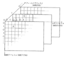
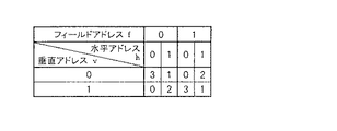
実施の形態1では水平アドレス発生回路12、垂直アドレス発生回路13、フィールドアドレス発生回路14に1ビットカウンタを導入した例について説明する。これによって例えば図3に示すように、水平・垂直アドレスは、画面上に複数存在し互いに同じ画素を共有しない2×2画素の各範囲内において、左上にある画素を基準としたときの相対的な空間座標を示し、フィールドアドレスは時間方向を2フィールドの周期で分割したときの周期内における相対的な時間座標を示すように設定される。図3において例えばAで示される位置・時刻においては、画素の水平・垂直・フィールドアドレスは、水平アドレスをh、垂直アドレスをv、フィールドアドレスをfとして、(h,v,f)=(0,1,0)と設定される。同じようにしてBで示される位置・時刻においては画素の水平・垂直・フィールドアドレスは、(h,v,f)=(1,0,1)と設定される。
【0043】
実施の形態1では、空間座標を特定するために、ディスプレイ画面上を互いに同じ画素を共有しない2×2画素の範囲に分割したが、このような空間座標を特定するために設定された複数画素で構成される範囲を以下特に「領域」と呼ぶ。ディスプレイ画面上を「領域」に分割する方法は2×2画素の範囲に限るものではなく、各「領域」毎に範囲が異なるものであってもよいし、各「領域」内の画素に対する水平・垂直アドレスの割り付け方も任意のものであってよい。なお、説明を簡単にするために、「範囲」を連続した画素(例えば、「2×2画素の範囲」は縦方向に連続した2画素及び横方向に連続した2画素からなる4画素)としているが、必ずしも連続している必要はない。
【0044】
図2に示した平均値演算回路15では逆ガンマ補正部4、ラインメモリA10から出力されるディジタル映像信号のうち、非表示となる映像信号成分である下位2ビットのディジタル信号と、ラインメモリB11から出力される非表示となる映像信号成分である2ビットのディジタル信号を用いて、縦方向に3画素、横方向に3画素にわたる3×3画素の範囲について重み付け平均値を計算する。
【0045】
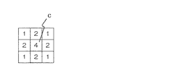
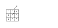
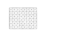
ここで、ある画素Cに関する重み付け平均値を求める場合について考える。図4は前述した3×3画素の範囲内の各画素に対する重み付けの例を示す図である。図において、画素Cそのものに対する重みは4、画素Cの上下左右の画素に対する重みは2、画素Cの左上、右上、左下及び右下の画素に対する重みは1を設定している。
【0046】
また、画素Cと画素Cに隣接する8画素について非表示となる映像信号成分が例えば図5のようになっているとする。すなわち、画素Cの非表示となる映像信号成分が3であり、画素Cの左隣、右上、左下にあたる画素の非表示となる映像信号成分がそれぞれ2、1、1であり、これ以外の5つの画素に関する非表示となる映像信号成分がすべて0とすれば、画素Cに関する重み付け平均値は、画素Cに関する非表示となる映像信号成分である3を重み4で乗じ(即ち、3×4=12)、画素Cの左隣の画素に関する非表示となる映像信号成分である2を重み2で乗じ(即ち、2×2=4)、画素Cの右上、左下の画素に関する非表示となる映像信号成分である1を重み1で乗じ(即ち、1×1=1)、その他の非表示となる映像信号成分は0であるので、これらの総和を求めることによって得られる重み付け総和18(12+4+1+1)を、重みの総和である16(4+2+2+2+2+1+1+1+1)で割った1.125の小数点第1位を四捨五入した値である1となる。なお、重み付け平均値に小数点以下の端数が出た場合には、実施の形態1では小数点第1位を四捨五入することとする。また、説明の簡単化のためになるべく10進表記を用いて説明しているが、実際のハードウェアにおいては一般に、これらの演算を2進方式(即ち、ディジタル方式)にて行っていることは言うまでもない。このようにして求められた重み付け平均値は図2のディザ信号発生回路16に出力される。
【0047】
実施の形態1では図2に示した平均値演算回路15において、重み付け平均値を求める演算を用いた例について示すが、これに限るものでなく、重みをすべて等しい値として平均値を求めてもよいし、重み付け総和を求めてもよい。重みをすべて等しい値として総和を求めるとしてもよい。以下、複数画素の非表示となる映像信号を重み付けして平均した値、重み付けをしないで平均した一般的な平均値、重み付けして総和した値、重み付けをしないで総和した値をそれぞれ単に「重み付け平均値」、「単純平均値」、「重み付け総和」、「総和」と称するとともに、このような演算値を総称して「平均値」と称することとする。なお、小数点以下の端数の処理についても任意のものであってよい。
【0048】
また、実施の形態1における図2の平均値演算回路15においては、図5に示したような画素Cを中心とした3×3画素の範囲内について平均値を求めるようにしているが、このような平均値を求める画素の範囲については任意に設定すればよい。すなわち、平均値を求める際の範囲(例えば、図5の3×3画素範囲)は、画素の空間座標を特定するために設定された範囲である「領域」(例えば、図3の2×2画素範囲)とは、独立に設定し得るものである。
【0049】
このようにして各画素は与えられた時間において、図2に示した水平アドレス発生回路12、垂直アドレス発生回路13、フィールドアドレス発生回路14、及び平均値演算回路15で行われる演算によって、水平アドレスh、垂直アドレスv、フィールドアドレスf、そして平均値aの4つの情報を持つことになる。ディザ信号発生回路16は、多段の選択器によって構成され、これら4つの情報を選択信号として、例えば図6のような1ビットのディザ信号を発生する。図は例えば(水平アドレスh,垂直アドレスv,フィールドアドレスf,平均値a)=(0,1,0,1)という空間座標、時間座標、及び平均値を持つ画素にはレベル0のディザ信号を、また(h,v,f,a)=(1,0,1,2)という空間座標、時間座標、及び平均値を持つ画素にはレベル1のディザ信号を発生することを意味する。なお、ここでの「レベル0のディザ信号を発生する」とは、ディザ信号を発生しないこと若しくはそれに同等の状態を意味し、「レベル1のディザ信号を発生する」とは、レベル0のディザ信号より大きい信号、特にここでは表示可能な映像信号成分に換算して1の大きさのディザ信号を発生することを意味する。
【0050】
図6では、画面上のどの画素においても平均値演算回路15の演算結果aが0以外の等しい値である場合には、縦方向に2画素おき、横方向に2画素おき、時間方向2フィールドおきにまったく同じディザ信号が加算されるようになっている。このように平均値演算回路15の演算結果aの各場合について設定されている1周期分のディザ信号のパターンを以下「ディザパターン」と呼ぶ。実施の形態1では横方向に2画素、縦方向に2画素、時間方向に2フィールドの周期を持つディザパターンを用いた例について説明するが、これに限るものではなく、任意の周期をもつディザパターンを採用することが可能である。また、実施の形態1では平均値演算回路15の演算結果aに対応して選択されるディザパターンの周期をすべて横方向に2画素、縦方向に2画素、時間方向に2フィールドという同じ周期を持つものとしたが、たとえば平均値が1であるときのみ横方向に4画素、縦方向に4画素、時間方向に4フィールドの周期をもつディザパターンを用いるなど、周期がディザパターンによって異なっていてもよい。
【0051】
前述のようなディザパターンにおける空間的な周期について説明する。例えば、図6においては、水平アドレス0及び1、並びに、垂直アドレス0及び1の範囲である2×2画素範囲がディザパターンの空間的な1周期である。さらに例えば、平均値演算回路15の演算結果aが3、フィールドアドレスfが0の場合に対して、2×2画素範囲のディザパターンの空間的な周期が設定され、(水平アドレスh,垂直アドレスv)=(0,0)に対してはレベル1のディザ信号が設定され、(h,v)=(1,0)に対してはレベル1が、(h,v)=(0,1)に対してはレベル0が、(h,v)=(1,1)に対してはレベル1のディザ信号が設定されている。
【0052】
このようなディザパターンが設定される画素の範囲(即ち、ディザパターンの空間的な周期)は、平均値を求める画素の範囲(例えば、図5の3×3画素範囲)や、画素の空間座標を特定するために設定された範囲である「領域」(例えば、図3の2×2画素範囲)とは、独立に設定し得るものである。
【0053】
図2に示した加算回路17では、ラインメモリA10から出力される、10ビットのディジタル映像信号のうち表示可能な映像信号成分である上位8ビットに対して、ディザ信号発生回路16で発生した1ビットのディザ信号を加算する。ディザ信号は8ビットの表示可能な映像信号成分の最下位ビットに加算される。このディザ信号が加算された8ビットの映像信号をフィールドメモリ部5に出力する。例えばディザ信号発生回路16においてレベル1のディザ信号が発生し、これを2進表記で(10010011)というレベルの8ビットの映像信号に加算する場合は、加算回路17の出力は(10010100)となる。
【0054】
以上のような構成で階調表現を行うディスプレイ装置では、ディスプレイ装置が本来持つ階調表現能力以上の階調を擬似的に表現することができ、階調が滑らかに変化する画像を忠実に再現することができる。これを図7乃至図9を用いて説明する。
【0055】
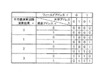
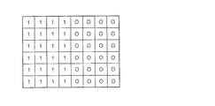
いま、縦方向に6画素、横方向に8画素を持つPDPに、滑らかに階調が変化する画像を表示する場合について考える。図7(a)は図2に示した逆ガンマ補正部4の出力である10ビットのディジタル映像信号と画素の対応関係を示す図である。すなわち、画面左上を基準として、縦1列目、2列目は0が本来表示すべき映像信号のレベルであり、以下同様に3、4列目は1が、5、6列目は2が、7、8列目は3が本来表示すべき映像信号のレベルであるとする。また、フィールドアドレスは0であるとする。
【0056】
なお図7(a)にはディスプレイ画面の外にある画素を仮想し、これらの画素に対応する映像信号も示している。図2に示した平均値演算回路15において重み付け平均値を求める際に、図7(a)の1列目、1行目、8列目、6行目にある画素については隣接する画素が8画素より少なくなるが、この場合は画面外にある仮想的な画素を用いて重み付け平均値を求める。例えば、1行1列目においては、1行1列目が0、その右隣、右下、及び下が0であるのに加え、右上、上、左上、左隣、及び左下の画素についても0という値を仮想して演算に利用する。これは水平又は垂直の有効な表示期間外にある映像信号も利用して重み付け平均値を求めることに相当する。
【0057】
図7(a)のようなA/D変換された映像信号について、図4に示した重み付けを行うと、図2の平均値演算回路15で求められる重み付け平均値は図7(b)のように各列にある画素同士で等しい値となり、2進数の小数点第1位まで求めたとすると、その値は1列目から8列目まで順に、0.0、0.0、0.5、1.0、1.5、2.0、2.5、3.0となる。例えば、図7(a)において1行2列目の画素は0である。右上、右隣、右下の画素は1である。その他、上、左上、左隣、左下、下は0である。よって、重み付け平均値は既に述べた計算によって((1×1+2×1+1×1)÷16)=0.25となる。ここで0.25は2進数で0.01であるから、小数点第1位まで求めて図7(b)のように0.0となる。なお、ここでは平均値を求める際、小数点第1位まで求めているが、さらに精度をあげてもよい。また、説明の簡単化のためなるべく10進表記で説明しているが、ハードウェア的には一般に、これらの演算を2進数のまま直接に計算していることは言うまでもない。
【0058】
実施の形態1では、前述したとおり図2に示した平均値演算回路15は小数点第1位を四捨五入するとしているので平均値演算回路15から出力される平均値は図7(c)のようになり、1列目から8列目まで順に0、0、1、1、2、2、3、3となる。
【0059】
したがって実際に表示される映像信号は前述した動作によって、図8(a)のようになる。また、図8(a)及び後述する図8(b)では図1及び2の多階調化処理部9の入出力端における映像信号を比較しやすくするために、8ビットの多階調化処理部9の出力に対して最下位ビットのさらに下位2ビットに0を挿入し、10ビットに変換した値を示している。このような方法による信号レベルの比較は多階調化処理部9の入出力を入出力端におけるそれぞれの最大レベルとの比をとることによって正規化された値で比較することとほぼ等しい。つまり、実施の形態1における多階調化処理部9の入力は10ビット(最大値1024)、出力は8ビット(最大値256)であるので、(入力値/1024)と(出力値/256)とを比較していることにほぼ等しい。さらに詳しくは、このような比較においては、10ビットのディジタル映像信号の4と、8ビットのディジタル映像信号の1とが等しい(4/1024=1/256)ことが示される。
【0060】
またディザ信号の加算法は1フィールドおきに異なるので、図8(b)に、図7(a)がフィールドアドレス1であった場合における実際に表示される映像信号を示す。
【0061】
図6に示されるディザパターンは1フィールドおきに異なるディザ信号を加算するようになっており、人間の視覚の時間的な積分効果によって、人間の目に実際に知覚される明るさは時間に対して平均化される。例えば、図8(a)のようなフィールドアドレス0における映像信号と、図8(b)のようなフィールドアドレス1における映像信号とが、視覚の時間的な積分効果によって図9に示すように平均化される。さらに1つ1つの画素は一般的に視覚的に十分小さく作られているので、人間の視覚の空間的な積分効果によってあたかも2×2画素の範囲内にある各画素が、その範囲内の映像信号の平均レベルで発光しているように知覚される。すなわちこの場合人間の目には、本来表示すべき映像である図7(a)とまったく同じ映像が再現されているように知覚される。
【0062】
なお厳密に述べると、実施の形態1においては、あるフィールドアドレス0のときに仮に平均値1に対するディザパターンが適用された場合であっても、次のフィールドアドレス1においても当該平均値1のディザパターンが適用されるとは限らない。画面の激しい切り替わり時においては、同一の画素であってもフィールドアドレス0と1で演算される平均値が異なり、適用されるディザパターンが異ってくることがあり得る。しかしながら、ディザ信号の加算が効果を奏するのは階調がゆるやかに変化する場合が中心であり、そのような画面の激しい切り替わりによる、前述のような近接するフィールドアドレス間における平均値の違いは問題とはならない。なお、階調が緩やかに変化する場合のみを選択してディザ信号を加算するなど、ディザ信号の加算を行う状況を任意に設定してもよい。
【0063】
このように実施の形態1であるディスプレイ装置では、ディスプレイ装置が本来表示できる最も低い映像信号成分の4分の1の映像信号成分までを擬似的に再現することができるので、ディスプレイの階調表現能力は擬似的には2ビット多い10ビットとなる。
【0064】
これに対して、従来のディスプレイ装置では、図7(a)に示したような非表示となる映像信号成分を含む表示例の場合、全画面が黒になってしまうため、正しく映像が再現されない。
【0065】
実施の形態2.
図10は実施の形態2である多階調化処理部9の詳細を示す図である。なお、実施の形態2ではディスプレイ装置の全体構成とその動作は実施の形態1において図1を用いて説明したものと同じであるので、これに関わる説明を省略する。さらに、実施の形態2であるディスプレイ装置の多階調化回路を説明するにあたり、図2に示したものと同一又は相当部分には同一符号を付し、説明を省略する。
【0066】
実施の形態2では、図10に示すようにセレクタ18を設け、逆ガンマ補正部4、ラインメモリA10、ラインメモリB11、水平アドレス発生回路12、垂直アドレス発生回路13の出力に基づいて、後述するような特定の2×2画素に関する非表示となる映像信号成分を選択し、平均値演算回路19に出力する。
【0067】
また、実施の形態2では、平均値演算回路19は複数画素で構成される範囲に関する「重み付け平均値」ではなく、一般的な平均値である「単純平均値」を演算する。
【0068】
次に、図10に示した多階調化処理部9の動作について説明する。
【0069】
逆ガンマ補正部4から出力された10ビットのディジタル映像信号はまずラインメモリA10に送られ、そこで1ライン分記憶される。次にラインメモリB11は、ラインメモリA10の出力のうち非表示となる映像信号成分である下位2ビットについて、やはり1ライン分記憶する。
【0070】
セレクタ18では逆ガンマ補正部4、ラインメモリA10、ラインメモリB11、水平アドレス発生回路12、及び垂直アドレス発生回路13の出力に基づいて、特定の2×2画素に関する非表示となる映像信号成分を選択し、平均値演算回路19に出力する。すなわち、ある画素Dが与えられたとき、画素Dの水平アドレスhと垂直アドレスvの組み合わせにより、図11(a)のように平均値演算回路19に出力する2×2画素を変える操作を行う。例えば画素Dの水平・垂直アドレスが(h,v)=(0,0)であれば、図10に示した平均値演算回路19に出力されるのは画素D40と、画素D40のそれぞれ右隣の画素41、1ライン下の画素42、右下の画素43の合計4つの画素に関する非表示となる映像信号成分である。同様に、画素Dの水平・垂直アドレスが(h,v)=(1,0)、(0,1)及び(1,1)のときも、画素40乃至画素43の4画素が図10に示した平均値演算回路19に出力される。
【0071】
平均値を演算する前に図10のセレクタ18でこのような操作を行うことにより、後述するように、画面上のすべての画素は、平均値を求める単位であり、画面上に複数個存在する2×2画素の範囲のいずれか1つに含まれることになる。これによって後述するように2×2画素の各範囲内の映像信号の平均レベルを多階調化処理部9の入出力端でほぼ等しくすることができ、映像をより忠実に再現することが可能となる。
【0072】
さらに平均値演算回路19では、セレクタ18から出力された2ビットの非表示となる映像信号成分の縦方向に2画素、横方向に2画素にわたる2×2画素の範囲について平均値を計算する。
【0073】
いま、ディザ信号発生部16では図6で示したものと同じディザパターンを発生するものとする。
【0074】
図6に示すように、フィールドアドレスが0である場合でも1である場合でも、すべての2×2画素の範囲について、図10のディザ信号発生回路16におけるディザパターンは平均値演算回路19から出力された平均値aと等価なディザ信号を出力するように構成されている。すなわち、平均値演算回路19から出力される2×2画素範囲における平均値aと、その2×2画素範囲に加算されるディザ信号の総和を範囲内の画素数である4で割った値とが、互いに等しくなっている。例えばフィールドアドレスfが0であり、平均値aが1である場合には、2×2画素の範囲内にある画素のうち水平アドレスh、垂直アドレスvが(h,v)=(0,0)である画素にのみレベル1のディザ信号が加算される。このディザ信号は多階調化処理部9の入力である10ビットのディジタル映像信号の下位3ビット目の位置に加算されるので、2×2画素の範囲に加算されるディザ信号のレベルの総和は10ビット換算で4に相当し、それを範囲内の画素数4で割った値は1となって平均値と等しい。なお、ここでは、平均値を求める範囲と、ディザ信号が加算される範囲とを、同一の2×2画素の範囲としたが、異なる画素範囲であってもよく、それぞれ独立に設定しうるものである。
【0075】
また、実施の形態2では、前述したような図10のセレクタ18における操作によって、平均値演算回路19では、互いに同じ画素を共有しない2×2画素の単位に分割されたディスプレイ画面上の各範囲についての平均値を求めることになるため、各2×2画素の範囲内にある4つの画素に関する平均値はすべて等しくなる。
【0076】
したがって、いかなる映像信号が逆ガンマ補正部4から出力されたとしても、平均値を求めるときに発生する誤差以外に、多階調化処理部9の入出力端で2×2画素の範囲内の映像信号の平均レベルを変化させる要因は原理的には存在しない。
【0077】
次に「部分領域」を定義する。実施の形態2では、非表示成分となる映像信号成分が2ビットである。即ち、図6に示したように、平均値演算回路19が四捨五入等の処理を行って演算する平均値aは、0、1、2、3のいずれかとなる。レベル0のディザ信号の場合には、ディザ信号発生回路16はディザ信号を発生しない、又はそれに同等であるので、ディザ信号発生回路16がディザ信号が発生する際の最小の平均値aは1である。これはディスプレイ装置が本来持つ階調表現能力である階調1の1/4に相当する。実施の形態2においてはディスプレイ装置が本来持つ階調表現能力よりも2ビット多い階調を擬似的に表現する(即ち、1/4階調までを擬似的に表現する)ために、「2×2画素範囲中の4画素のうち、1画素にはディザ信号1を加算し、残りの3画素にはディザ信号を加算しない」ようにした例である。以下、このような擬似的階調表現をするための最小の単位となる範囲を、特に「部分領域」と呼ぶ。
【0078】
実施の形態2では、ディスプレイ装置が本来持つ階調表現能力である階調1の1/4階調を表現するために、2×2画素範囲の4画素を一つのまとまりとして扱い、その4画素の範囲において、「一定の時間」同一のディザパターンが適用される場合(即ち、演算される平均値aが一定の時間等しい場合)、当該範囲における非表示となる映像信号成分の平均値(この例では平均値a=1)と当該範囲の画素の上位8ビットに対して加算されるディザ信号の平均値とが、10ビットに換算したときに略等しくなるようにディザパターンが設定されている。この例では10ビット換算の平均値aが1であり、当該範囲に加減算されたディザ信号の10ビット換算の平均値が4/4画素=1で等しい。なお、上述のような所定の範囲におけるディザ信号の平均値を、以下特に「平均レベル」と称する。
【0079】
すなわち実施の形態2は、擬似的階調表現をするための最小の単位となる範囲である「部分領域」において、「一定の時間」同一のディザパターンが適用される場合に、当該範囲における非表示となる映像信号成分の平均値と当該範囲の画素に対して加算されるディザ信号の平均レベルとが、同一のビット数に換算したときに略等しくなるようにしたものであり、特にここでは前述の「一定の時間」を1フィールドとし、「部分領域」である2×2画素の範囲に関して平均値を求めている。
【0080】
実施の形態2では特に「部分領域」を実施の形態1で定義された「画素の空間座標を特定する」ための「領域」と同じ2×2画素の範囲としているが、必ずしも同じ範囲とする必要はない。また、実施の形態2では図6に示したディザパターンの空間的な周期を「部分領域」と同じ2×2画素の範囲としているが、必ずしも同じ範囲とする必要はなく、複数の「部分領域」からなるディザパターンを設定してもよい(例えば、2×2画素範囲の「部分領域」4つからなる4×4画素範囲の空間的周期をもつディザパターンを設定してもよい)。
【0081】
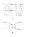
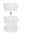
さらに例えば、いま、図11(b)に示すような2×2画素の範囲があるとする。左上画素、右上画素、左下画素、及び右下画素の非表示となる映像信号成分である下位2ビットがそれぞれ2、1、1、3である。また、(水平アドレスh,垂直アドレスv,フィールドアドレスf)は、左上画素が(0,0,1)、右上画素が(1,0,1)、左下画素が(0,1,1)、右下画素が(1,1,1)である。なお、表示可能な映像信号成分である上位8ビットはすべて0であるとする。
【0082】
図10に示した水平アドレス発生回路12及び垂直アドレス発生回路13が図11(b)の左上画素(0,0,1)を選択している場合には、セレクタ18は図11(b)の左上画素2、右上画素1、左下画素1、右下画素3を選択する。図10の平均値演算回路19は、この平均値((2+1+1+3)÷4)を演算するとともに、それを四捨五入した2をディザ信号発生回路16に出力する。平均値2が入力されたディザ信号発生回路16は、図6に示したディザパターンに基づき(水平アドレスh,垂直アドレスv,フィールドアドレスf,平均値演算回路演算結果a)=(0,0,1,2)よりレベル0のディザ信号を発生する。
【0083】
次に図11(b)の右上画素(1,0,1)について考えると、図11(a)に示したような画素の選択方法によって、前述したような左上画素(0,0,1)が選択されている場合と全く同様に、図11(b)の左上画素2、右上画素1、左下画素1、右下画素3が選択され、求められる平均値も同様の2になる。よって、図6のディザパターンに基づき(水平アドレスh,垂直アドレスv,フィールドアドレスf,平均値演算回路演算結果a)=(1,0,1,2)よりレベル1のディザ信号を発生する。同様に、左下画素(0,1,1,2)についてはレベル1のディザ信号、右下画素(1,1,1,2)についてはレベル0のディザ信号を発生する。
【0084】
図11(b)に示す2×2画素範囲について、1フィールド期間の非表示となる映像信号成分である下位2ビットの総和を求めると7(2+1+1+3)であり、これは10ビットに換算しても7である。一方、当該範囲内の各画素に対して1フィールド期間に発生したディザ信号の総和は2(0+1+1+0)、即ち、10ビットに換算すると2表記で(0000001000)となり8である。つまり、2×2画素範囲の「部分領域」内の各画素の非表示成分の総和7と、当該「部分領域」内の各画素について発生した1フィールド期間あたりのディザ信号の総和8とが10ビットに換算して略等しい。なお、同一とならないのは、図10の平均値演算回路19が平均値を計算する際に四捨五入等の処理を行うためである。
【0085】
以上のような、実施の形態2における階調表現方法によって滑らかに階調が変化する画像を正しく再現できることは、前記図7(a)のような映像を表示した場合を考えれば明らかである。この場合前述した動作により、実施の形態1とまったく同じ結果が得られる。
【0086】
実施の形態3.
実施の形態3はディザ信号発生回路16の構成・動作が実施の形態2と異なる場合についての例である。
【0087】
図12は実施の形態3であるディザ信号発生回路16の詳細を示す図である。ディザ信号発生回路16以外の構成は実施の形態2と同様であるので、説明を省略する。
【0088】
図12のディザ信号発生回路16は図10に示した平均値演算回路19の出力である平均値aに、水平アドレス発生回路12の出力である水平アドレスh、垂直アドレス発生回路13の出力である垂直アドレスv、フィールドアドレス発生回路14の出力であるフィールドアドレスfによって異なるパターンを加算することで、ディザ信号を発生する。図12において20は空間座標と時間座標から所定の2ビットの信号パターンを発生するパターン発生器、21は平均値演算回路19の出力である平均値aにパターン発生器20で発生した信号を加算する加算器である。加算器21の出力は3ビット(即ち、0から6)であるが、このうち下位2ビットを切り捨て、上位1ビットのみをディザ信号として加算回路17に出力する。
【0089】
次に、ディザ信号発生回路16を構成する各部の動作について説明する。
【0090】
図13は図12に示したパターン発生器20で発生する信号パターンの例である。すなわち、水平アドレスh、垂直アドレスv、フィールドアドレスfの組み合わせが、例えば(h,v,f)=(0,0,0)という空間座標と時間座標を持つ画素にはレベル3の信号を発生し、(h,v,f)=(1,0,1)という空間座標と時間座標を持つ画素にはレベル2の信号を発生する。
【0091】
一方、図12の加算器21では、平均値演算回路19で求めた平均値aと、パターン発生器20で発生した信号とを加算し、演算結果の上位1ビットのみを加算回路17に出力する。例えば、平均値aが2である画素に対してパターン発生器20にてレベル3の信号が発生した場合にはディザ信号は2に3加算した5、すなわち2進表記で(101)の上位1ビットである1を出力する。
【0092】
このような操作によって発生するディザ信号は、実施の形態2で発生するディザ信号とまったく同じである。したがって実施の形態3では実施の形態2とまったく同様の効果が得られる。
【0093】
実施の形態3では平均値と信号パターンとを加算する加算器21を設けたが、これに限らず例えば加算器の代わりに平均値と信号パターンとを比較する比較器を設け、平均値がパターン発生器20で発生した信号以上のレベルを持つときのみレベル1のディザ信号を出力し、それ以外のときはレベル0のディザ信号を発生するとしても同様の効果が得られる。
【0094】
実施の形態4.
図14は実施の形態4である多階調化処理部9の詳細を示す図である。なお、実施の形態4ではディスプレイ装置の全体構成とその動作は実施の形態1において図1を用いて説明したものと同じであるので、これに関わる説明を省略する。さらに、実施の形態4であるディスプレイ装置の多階調化回路を説明するにあたり、図2に示したものと同一又は相当部分には同一符号を付し、説明を省略する。
【0095】
実施の形態4ではラインメモリの代わりに1画素分の情報を記憶するレジスタを2つ用いる。すなわち図14に示したレジスタA22と、レジスタB23を用いる。またセレクタ24は逆ガンマ補正部4、レジスタA22、レジスタB23、水平アドレス発生回路12の出力に基づいて、後述するような特定の2×1画素に関する非表示となる映像信号成分を選択し、平均値演算回路19に出力する。
【0096】
逆ガンマ補正部4の出力である10ビットのディジタル映像信号はまずレジスタA22に送られ、そこで1画素分記憶される。
【0097】
また、レジスタB23はレジスタA22の出力のうち非表示となる映像信号成分である下位2ビットについてやはり1画素分記憶する。レジスタA22、レジスタB23により、ある画素Eが与えられたとき、画素Eとその左右2画素の合計3画素について非表示となる映像信号成分を一度に知ることができる。
【0098】
セレクタ24では逆ガンマ補正部4、レジスタA22、レジスタB23、及び水平アドレス発生回路12の出力に基づいて、特定の2×1画素に関する非表示となる映像信号成分を選択し、平均値演算回路19に出力する。すなわち画素Eの水平アドレスが0であれば、画素Eと画素Eの右隣にある画素についての平均値をとり、画素Eの水平アドレスが1であれば、画素Eと画素Eの左隣にある画素についての平均値をとるようにする。例えば、画素Eの水平アドレスが1であり、画素Eの非表示となる映像信号成分が2進表記で(10)であり、その左隣の画素の非表示となる映像信号成分が2進表記で(00)であれば、画素Eとその左隣にある画素に関する平均値は10進数で1となる。これにより、画面上のすべての画素は、画面上に複数個存在する平均値を求める単位である2×1画素の範囲のいずれか1つに含まれることになる。以下、平均値を求めるために設定した範囲同士が互いに同じ画素を共有しないときに、この各範囲を「単位領域」と呼ぶ。
【0099】
これ以外の部分の動作については実施の形態1と同じである。
【0100】
ディザ信号発生回路16では図6に示したディザパターンを発生するが、実施の形態2で前述したとおり、図6に示すディザパターンではいずれも2×2画素の範囲が実施の形態2で定義した「部分領域」となる。したがって、2×1画素に関する平均値によってディザ信号発生回路16を動作させる場合は、「部分領域」内に加算されるディザ信号は実施の形態2と必ずしも一致しない。
【0101】
例えば、フィールドアドレスが0の時刻においてある2×2画素の範囲内の左上、右上、左下、右下の画素に関する非表示となる映像信号成分がそれぞれ3、3、1、1であり、左上の画素の水平アドレスhと垂直アドレスvが(h,v)=(0,0)であるとする。このとき実施の形態4では、図6で示されるディザパターンに基づいて、左上と右上の画素の2つの画素にディザ信号が加算される。実施の形態2では、2×2画素の範囲内に関する平均値である2を求め、この場合には左上と右下の画素にディザ信号が加算されるので、実施の形態2と実施の形態4は必ずしも結果は一致しない。
【0102】
しかし、表示すべき映像が前記図7(a)のように、1つの「部分領域」を構成する各「単位領域」において平均値が等しい場合には、実施の形態2とまったく同じ結果が得られる。すなわちラインメモリを2個省略することによって回路を簡略化し、平均値を求める範囲を、「部分領域」よりも小さくしたとしても、滑らかに階調が変化する画像を忠実に再現することが可能であり、実施の形態2と同様な効果を得ることができる。
【0103】
以上のような実施の形態4においては、平均値を求める範囲は2×1画素範囲の「単位領域」であり、「部分領域」は2つの「単位領域」を含む2×2画素範囲である。そして、2つの「単位領域」の非表示成分の平均値が等しいとき、当該「単位領域」における非表示となる映像信号成分の平均値と、当該「部分領域」において加算されるディザ信号の平均レベルとが10ビットに換算して略等しくなるようにディザパターンが構成されており、これによって画像を忠実に再現することが可能である。
【0104】
実施の形態5.
実施の形態5ではディスプレイ装置が本来持つ階調表現能力よりも4ビット多い階調を擬似的に表現する例について考える。実施の形態5であるディスプレイ装置の構成は、実施の形態2である図1、図10に示したものと同様の構成をとるので図示することを省略し、4ビット多い階調を表現するために実施の形態2とは異なる点について説明する。
【0105】
図10において逆ガンマ補正部4からは12ビットのディジタル映像信号が出力されるものとし、逆ガンマ補正部4から出力された12ビットのディジタル映像信号はまずラインメモリA10に送られ、そこで1ライン分記憶される。
【0106】
次にラインメモリB11は、ラインメモリA10の出力のうち非表示となる映像信号成分である下位4ビットについて、やはり1ライン分記憶する。
【0107】
また水平アドレス発生回路12、垂直アドレス発生回路13、フィールドアドレス発生回路14にはそれぞれ2ビットカウンタを用い、2ビットの水平アドレス、垂直アドレス、フィールドアドレスを出力する。
【0108】
セレクタ18は実施の形態2で行ったものと同様の操作を水平アドレス発生回路12、垂直アドレス発生回路13のそれぞれ下位1ビットだけを参照して行う。セレクタ18の出力は2×2画素の範囲内の4つの画素に関する非表示となる映像信号成分である4ビットのディジタル信号である。
【0109】
さらに平均値演算回路19では、セレクタ18から出力された4ビットの非表示となる映像信号成分を縦方向に2画素、横方向に2画素にわたる2×2画素の範囲について平均値を計算する。すなわち、実施の形態5では「単位領域」は2×2画素の範囲となる。
【0110】
ディザ信号発生回路16では、水平アドレス発生回路12、垂直アドレス発生回路13、フィールドアドレス発生回路14から出力される2ビットの水平アドレスh、垂直アドレスv、フィールドアドレスfと、平均値演算回路19から出力される4ビットの平均値aに基づいて、図15に示すようなディザパターンを発生する。図では煩雑を避けるために平均値aが1の場合についてのみ示している。これ以外の、平均値aが0,2,3,4,5,6,7,8,9,10,11,12,13,14,15となる場合に発生するディザパターンについては図示することを省略するが、これらは任意のものであってよい。例えば平均値aが4,8,12となるときは図6で示した平均値aがそれぞれ1,2,3となるときに選択されるものとまったく同じディザパターンを発生するとしてもよい。この場合平均値aが4,8,12であるときには水平アドレスh、垂直アドレスv、フィールドアドレスfのそれぞれ下位1ビットのみを参照してディザ信号を発生することになる。なお、図15に示した平均値aが1の場合には、2ビットすべてを用いる。
【0111】
図10に示した加算回路17では、逆ガンマ補正部4から出力された12ビットのディジタル映像信号のうち表示可能な映像信号成分である上位8ビットに対して、ディザ信号発生回路16で発生したディザ信号を加算する。ディザ信号は8ビットの表示可能な映像信号成分の最下位ビットに加算される。
【0112】
平均値演算回路19から出力される平均値aが1のときにディザ信号発生回路16で発生するディザパターンは、図15を見れば分かるように、4×4画素の範囲内に2フィールドの期間このディザパターンが適用された場合にのみ、平均値と加算するディザ信号の平均レベルが一致するように構成されている。すなわち4×4画素の範囲内に加算されるディザ信号の平均レベルは、フィールドアドレスが0と2の時刻では12ビット換算で2となり、フィールドアドレスが1と3の時刻では12ビット換算で0となってどちらも平均値1と等しくならないが、フィールドアドレス0と1またはフィールドアドレスが2と3の2フィールドの期間にわたる4×4画素の範囲内に加算されるディザ信号の平均レベルは1となって平均値と等しくなる。
【0113】
実施の形態5は4×4画素が「部分領域」となり、1つの「部分領域」が4つの「単位領域」から構成され、2フィールドの期間で「部分領域」内の平均値とディザ信号の平均レベルが等しくなる場合についての例である。さらに述べると、実施の形態5においてはディスプレイ装置が本来持つ階調表現能力よりも4ビット多い階調を擬似的に表現する(即ち、1/16階調までを擬似的に表現する)ために、例えば「16画素のうち、1画素にはディザ信号1を加算し、残りの15画素にはディザ信号を加算しない」というようにする例であり、特に、そのようなディザ信号の加算を、視覚の空間的、時間的な積分効果が働きやすいようなディザパターンを用いて行うものである。
【0114】
図10に示したディザ信号発生回路16で発生するディザパターンは、図16のように各フィールド内で平均値とディザ信号の平均レベルとが等しくなるように構成してもよいが、この場合には4×4画素という比較的広い範囲において1つしかないディザ信号の加算位置がフィールド毎に移動するので、特に画素を視覚的に小さく作ることが比較的困難なPDPなどでは、視覚の空間的な積分効果が働きにくく、ディザ信号の加算位置がフィールド毎に移動しているのがそのまま知覚され、映像の再現性が劣化する。
【0115】
これに対して図10に示したディザ信号発生回路16において発生するディザパターンを図15のように構成すると、4×4画素の範囲内の2画素について1度にディザ信号が加算されるため、図16のディザパターンを用いた場合に比べ視覚の空間的な積分効果が働きやすい。
【0116】
ここで、図15では4×4画素の範囲内に加算されるディザ信号の平均レベルは、フィールド毎に2と0という異なる値を取るため、視覚の時間的な積分効果は働きにくくなり、特に静止画を表示するときなどはフィールド毎に異なる明るさがフリッカとして知覚されやすいが、図10に示した平均値演算回路19から出力される平均値が1のときにはディザ信号の加算によって再現すべき非表示となる映像信号成分のレベルは、ディスプレイで表示可能な最低の信号レベルの16分の1と小さいため、フリッカの程度は十分低く映像の再現性は図16を用いた場合に比べて優れている。
【0117】
実施の形態5では2フィールドで「部分領域」内の平均値とディザ信号の平均レベルが等しくなるようなディザパターンを構成したが、これに限らずfフィールド(fは2以上の整数)で平均値とディザ信号の平均レベルが等しくなるようなディザパターンを構成するとしてもよい。
【0118】
以上のように実施の形態5においては、平均値を求める範囲は2×2画素範囲の「単位領域」であり、「部分領域」は4つの「単位領域」を含む4×4画素範囲である。そして、2フィールドにわたって、この「部分領域」を構成する各「単位領域」における非表示となる映像信号成分の平均値がそれぞれ略等しいとき(この例では、のべ8個の「単位領域」の平均値が略等しいとき)、当該「部分領域」内において、ディザ信号加算前の非表示となる映像信号成分の平均値と、加算されるディザ信号の平均レベルとが12ビットに換算して略等しくなるようにディザパターンが構成されており、これによって画像を忠実に再現することが可能である。
【0119】
実施の形態6.
図17は実施の形態6である多階調化処理部9の詳細を示す図である。なお、実施の形態6ではディスプレイ装置の全体構成とその動作は実施の形態1において図1を用いて説明したものと同じであるので、これに関わる説明を省略する。さらに、実施の形態6であるディスプレイ装置の多階調化回路を説明するにあたり、図2に示したものと同一又は相当部分には同一符号を付し、説明を省略する。
【0120】
図17において、25は水平アドレス発生回路12、垂直アドレス発生回路13、フィールドアドレス発生回路14、及び平均値演算回路19の各出力、並びに外部から入力されるディザパターン選択信号44に基づいて、後述するように発生すべきディザパターンを選択するディザ信号発生回路である。
【0121】
ディザ信号発生回路25は、平均値演算回路19から出力される平均値aが1である場合には、図18に示すディザパターンAとディザパターンBの2通りのディザパターンを発生する。この2つのディザパターンの選択は図17のディザパターン選択信号44によって行う。平均値が0,2,3となる場合に発生するディザパターンについては図示することを省略するが、これらは任意のものであってよい。ディザパターンBは4フィールドの周期を持っているのでフィールドアドレス発生回路14には2ビットカウンタを用い、ディザパターンAを用いるときにはフィールドアドレスの下位1ビットのみを参照するものとする。
【0122】
これ以外は実施の形態2と同じである。
【0123】
ディザパターン選択信号は,表示すべき映像が静止画であるときにはディザパターンAを選択し、反対に動画を表示するときにはディザパターンBを選択するようにディザ信号発生回路25に要求する。静止画と動画の判別法は任意であるが、例えば同期信号を拠り所として、パソコンなどの画面を表示する場合はぼぼ静止画であるとし、放送局から送られてくる映像は動画であるとする判別を行ってもよいし、映像の動きを直接検出することによって判別を行い、加算すべきディザパターンを決定してもよい。
【0124】
ディザパターンAは図6で説明したものと同一のディザパターンであり、このディザパターンが階調が滑らかに変化するような静止画を忠実に再現することができることはすでに実施の形態2で述べた通りである。
【0125】
ここで、ディザパターンBを動画を表示するときに選択する理由を説明するにあたり、図19乃至図21を用いる。
【0126】
図7(a)で用いたものと同じ縦方向に6画素、横方向に8画素を持つPDPを考え、このPDPに暗い縦帯を表示した場合について考える。すなわち、図17の逆ガンマ補正部4の出力端においては、図19に示すように10ビットのディジタル映像信号のレベルが縦1列目から4列目までは1となっており、この1というレベルの暗い縦帯が本来表示すべき映像信号であるとする。
【0127】
ここでさらにこの暗い縦帯が画面の右方向に1フィールドあたり1画素の割合で画面上右方向に移動しているとする。したがって時刻0において暗い縦帯が縦1列目から4列目まで表示されていたとすると、時刻0から4フィールド後には縦5列目から8列目に暗い縦帯が表示されることになる。
【0128】
このような映像を図18に示したディザパターンAを用いて表示すると、図20(a)乃至(b)のようになる。ただし図では簡単のため暗い縦帯が表示されている部分のみを示し、図8(a)及び(b)で行ったように図17に示した多階調化処理部9の出力である表示可能な映像信号成分を10ビットに換算した値で示している。この場合、暗い縦帯の動きに完全に追随して映像を観測している人には、各フィールドで表示されているレベルは平均化され、図20(c)に示すような2本の縦線状の固定パターンとして観測される。このようにディザパターンAでは動画の場合には静止画に比べて映像の再現性が劣化する。
【0129】
これに対して、図18に示したディザパターンBを用いて表示すると各時刻に表示されている映像と、4フィールド分の映像を平均化した映像は図21のようになり、暗い縦帯の動きに完全に追随して映像を観測している人にも、固定パターンは知覚されず、本来表示すべき映像が忠実に再現されるようになる。
【0130】
しかし静止画を表示する際には4フィールドという比較的長い周期を持つディザパターンBでは視覚の時間的な積分効果が働きにくく、特に表示すべき映像が暗い場合などは、ディザ信号の加算位置がフィールド毎に移動しているのが知覚されやすい。
【0131】
このように複数のディザパターンを用意し、表示すべき映像毎に最適なディザパターンを選択することによって、映像の再現性を高めることが可能である。
【0132】
実施の形態7.
図22は実施の形態7である多階調化処理部9の詳細を示す図である。なお、実施の形態7ではディスプレイ装置の全体構成とその動作は実施の形態1において図1を用いて説明したものと同じであるので、これに関わる説明を省略する。さらに、実施の形態7であるディスプレイ装置の多階調化回路を説明するにあたり、図2に示したものと同一又は相当部分には同一符号を付し、説明を省略する。
【0133】
実施の形態7は実施の形態5と同様に、ディスプレイ装置が本来持つ階調表現能力よりも最大で4ビット多い階調を擬似的に表現する例について考える。以下に実施の形態5と異なる部分について説明する。
【0134】
図22において、26はラインメモリA10から出力される12ビットのディジタル映像信号のレベルと後述する閾値を比較し、その比較結果をディザ信号発生回路27に出力する付加ビット数選択回路である。
【0135】
ディザ信号発生回路27においては、16通りのディザパターンが用意されており、水平アドレス発生回路12、垂直アドレス発生回路13、フィールドアドレス発生回路14、及び平均値演算回路19の出力、並びに付加ビット数選択回路26の比較結果に基づいて、ディザ信号を発生する。
【0136】
次に付加ビット数選択回路26の動作について説明する。付加ビット数選択回路26ではディスプレイで表示できる最も低い映像信号成分の1倍に相当する16と、2倍に相当する32とを閾値として、逆ガンマ補正部4から出力される12ビットのディジタル映像信号が0から15の間であるときには(00)、16から31であるときは(01)、32以上の場合は(10)という2ビットのディジタル信号をそれぞれディザ信号発生回路27に出力する。
【0137】
ここでディザ信号発生回路27で発生する16通りのディザパターンは、実施の形態5と同じであるとする(例えば、図15)。実施の形態7では以降の説明において混同を避けるため、実施の形態5で用いた、16通りの平均値に対応して選択されるディザパターンに0から15までの番号をつける。例えば、実施の形態5において平均値が3のときに選択されるディザパターンには3番という番号をつけ、平均値が12のときに選択されるディザパターンには12番という番号をつける。
【0138】
ディザ信号発生回路27では、水平アドレス発生回路12、垂直アドレス発生回路13、フィールドアドレス発生回路14、及び平均値演算回路19の出力、並びに、付加ビット数選択回路26の比較結果に基づいてディザ信号を発生する。すなわち、付加ビット数選択回路26の出力が(00)である場合には、平均値と同じ番号を持つディザパターンを選択し、(01)である場合には、平均値が0、1であるときには0番、平均値が2、3であるときには2番、平均値が4、5であるときには4番、平均値が6、7であるときには6番、平均値が8、9であるときには8番、平均値が10、11であるときには10番、平均値が12、13であるときには12番、平均値が14、15であるときには14番のディザパターンをそれぞれ選択し、(10)である場合には平均値が0、1、2、3であるときには0番、平均値が4、5、6、7であるときには4番、平均値が8、9、10、11であるときには8番、平均値が12、13、14、15であるときには12番のディザパターンを選択する。
【0139】
以上の操作により、逆ガンマ補正部4から出力される映像信号のレベルが、ディスプレイで表示できる最も低い信号レベルの1倍未満であるときには、選択可能なディザパターンは0番から15番までの各ディザパターンとなるので、このときにはディスプレイ装置が本来持つ階調表現能力よりも4ビット多い階調を擬似的に表現することが可能であり、また、映像信号のレベルがディスプレイで表示できる最も低い信号レベルの1倍以上2倍未満であるときには、選択可能なディザパターンは0,2,4,6,8,10,12,14の各ディザパターンとなるので、このときにはディスプレイ装置が本来持つ階調表現能力よりも3ビット多い階調を擬似的に表現することが可能であり、映像信号のレベルがディスプレイで表示できる最も低い信号レベルの2倍以上であるときには、選択可能なディザパターンは0,4,8,12の各ディザパターンとなるので、このときにはディスプレイ装置が本来持つ階調表現能力よりも2ビット多い階調を擬似的に表現することが可能である。
【0140】
このように擬似的な階調表現能力を映像信号のレベルに応じて変化させたことの効果について以下に述べる。
【0141】
人間の視覚は暗部の階調識別能力の方が明部のそれよりも高いため、ディスプレイ装置においても暗部の階調表現能力を特に高くする必要がある。しかし、一般にディザ信号の加算によって再現すべき映像信号成分のレベルが低ければ低いほど、固定パターンやフリッカなどの弊害が少ないディザパターンを構成することは困難になる。
【0142】
したがって、ディザ信号を加算することによる弊害よりもディスプレイの擬似的な階調表現能力の方が優先される暗部側では、より低い映像信号成分のレベルを再現できるようにし、ディスプレイの擬似的な階調表現能力よりもディザ信号を加算することによる弊害の方が問題となる明部側では、低い映像信号成分の再現精度を落とすことにより、全体的な画質を損なうことなく、人間の視覚特性にあった階調表現を行うことができる。
【0143】
実施の形態7ではディスプレイの擬似的な階調表現能力を2つの固定値を閾値として変化させたが、閾値のレベル、個数などはこれに限らず任意の値でよい。また閾値を固定値とせず、表示する映像の全体的な明るさや時間などに基づいて動的に変化させても同様の効果が得られる。
【0144】
実施の形態8.
図23は実施の形態8である多階調化処理部9の詳細を示す図である。なお、実施の形態8ではディスプレイ装置の全体構成とその動作は実施の形態1において図1を用いて説明したものと同じであるので、これに関わる説明を省略する。さらに、実施の形態8であるディスプレイ装置の多階調化回路を説明するにあたり、図2に示したものと同一又は相当部分には同一符号を付し、説明を省略する。
【0145】
図23において、28はラインメモリA10から出力される10ビットの映像信号を1ライン分記憶するラインメモリB、29は逆ガンマ補正部4、ラインメモリA10、ラインメモリB28から出力される10ビットの映像信号から、水平アドレス発生回路12、垂直アドレス発生回路13の出力に基づいて、実施の形態2の図11(a)で説明したものと同様な操作によって、特定の2×2画素に関する10ビットの映像信号を選択し、後述する信号成分抽出回路30に出力するセレクタである。
【0146】
図24は信号成分抽出回路30の詳細を示す図である。
【0147】
図において、映像信号48は注目する画素に関する映像信号であり、映像信号45、映像信号46、映像信号47は平均値を求めるべき画素と隣接する、同じ2×2画素の範囲内に存在する3つの画素に関する映像信号である。これらの映像信号はすべてセレクタ29より出力される信号である。
【0148】
また32は映像信号48からそれぞれ映像信号45、映像信号46、映像信号47を減算する3個の減算器、33はある決まった閾値を発生する閾値発生回路、34は減算器32の出力の絶対値と閾値発生回路33で発生した閾値とを比較し、減算器32の出力が閾値発生回路33で発生した閾値以下のときはレベル1を、そうでないときはレベル0を出力する3個の比較器、35は映像信号45、映像信号46、映像信号47のうち非表示となる映像信号成分である2ビットの信号成分の各ビットと比較器34の出力との論理積を出力する3個のAND回路、36は比較器34の出力に基づいて、映像信号48との差が閾値発生回路33で発生した閾値以下となっている映像信号を持つ画素の数を特定する画素数取得回路である。
【0149】
これより、図の信号成分49は、映像信号48と映像信号45の差の絶対値がある閾値以下のときには映像信号45の非表示となる映像信号成分である下位2ビットとなり、映像信号48と映像信号45の差の絶対値がある閾値より多いときには2ビットでレベル0の信号となる。これは信号成分50、信号成分51についても同様で、それぞれ映像信号46、映像信号47の下位2ビット、または2ビットのレベル0の信号となる。信号成分52については必ず映像信号48の非表示となる映像信号成分である下位2ビットが出力される。また図の画素数53は映像信号45、映像信号46、映像信号47がいずれも映像信号48とある閾値より大きい差をもつときには1を、いずれか1つが映像信号48と閾値以下の差であるときには2を、3つのうち2つが映像信号48と閾値以下の差であるときには3を、3つすべてが閾値以下の差であるときには4となる。これら信号成分49、信号成分50、信号成分51、信号成分52、画素数53の値はすべて平均値演算回路31に出力される。
【0150】
平均値演算回路31では信号成分抽出回路30の出力である、信号成分49、信号成分50、信号成分51、信号成分52の総和を求め、それをやはり信号成分抽出回路30の出力である画素数53で除算する。
【0151】
このような信号成分抽出回路30、平均値演算回路31における演算を例をあげて具体的に説明する。ある2×2画素について、左上にある画素に関する映像信号が10ビットで0であり、右上にある画素に関する映像信号が10ビットで1であり、左下にある画素に関する映像信号が10ビットで2であり、右下にある画素に関する映像信号が10ビットで32である場合を考える。このとき閾値発生回路33には10ビットで16という値が設定されているものとする。
【0152】
左上、右上、左下の画素に関する平均値はいずれも左上、右上、左下の画素に関する非表示となる映像信号成分の総和である3を画素数の3で割った1である。ここで左上、右上、左下の画素に関する平均値を求めるときに右下の画素を除外するのは左上、右上、左下の画素に関する映像信号のレベルと右下の画素に関する映像信号のレベルの差の絶対値が閾値である16よりも大きいからである。したがって同様な理由により、右下の画素に関する平均値は、右下の画素に関する非表示となる映像信号成分である0を画素数の1で割った0となる。
【0153】
これ以外の部分の構成、動作については実施の形態2と同様である。
【0154】
実施の形態7において、図23に示した信号成分抽出回路30、平均値演算回路31によって実現される演算により、階調がなだらかに変化している部分のみを抽出して平均値を求めることができる。このようにして求められた平均値に基づいてディザ信号を加算することにより、画像をより忠実に再現することが可能である。
【0155】
このことは、例えば黒の背景に1画素の幅を持つ縦線を画面上に表示する場合について考えてみれば非常に明らかである。この場合、実施の形態2であるディスプレイ装置では、縦線に隣接する本来は黒が表示されるはずの画素にディザ信号が加算されてしまうが、実施の形態7であるディスプレイ装置では、閾値を適切に設定することによりこのようなことは起こらない。
【0156】
実施の形態9.
実施の形態9は図1の逆ガンマ補正部4の構成、動作が実施の形態2と異なる場合についての例である。また実施の形態9では、A/D変換部3では入力された映像信号を8ビットのディジタル映像信号に変換して出力し、逆ガンマ補正部4は10ビットのディジタル映像信号を出力するとする。
【0157】
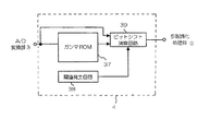
実施の形態9では、逆ガンマ補正部4で行われる演算をROMで実現する。すなわち、逆ガンマ補正部4の入力をROMのアドレスとして、そのアドレスに書き込まれているデータを読み出すことによって逆ガンマ補正を行うとする。
【0158】
図25は実施の形態9である逆ガンマ補正部4の構成を示す図である。図において、37はA/D変換部3から出力された8ビットのディジタル信号に対してガンマ補正の逆補正を行うガンマROM、38はある1つの閾値を発生する閾値発生回路、39はガンマROM37の出力である8ビットのディジタル信号に対して後述するようなビットシフト演算を行うビットシフト演算回路である。ここでガンマROM37は8ビットのアドレスを持ち、各アドレスに対して8ビットのデータを読み出せるものとする。
【0159】
逆ガンマ補正部4は放送局側で撮影された明るさをPDPなどのディスプレイ装置において再現するために必要な演算を行うが、一般にこの演算は、逆ガンマ補正部4の入出力のレベルをそれぞれの最大のレベルで正規化したときに、出力値が入力値の2.2乗となるようにする。例えばガンマROM37に入力される映像信号のレベルが8ビットで109であるときには、ガンマROM37の入力の最大レベルが255であるので、109を255で除算し、2.2乗した値がガンマROM37の出力をガンマROM37の出力の最大レベルで正規化した値となる。
【0160】
ここで、A/D変換部3から出力される映像信号のレベルが8ビットで128未満であるときは逆ガンマ補正の本来の演算結果を2ビット左シフトした値をガンマROM37にあらかじめ書き込んでおくようにする。例えばA/D変換部3から出力される映像信号のレベルが8ビットで109であるときには、ガンマROM37の出力は10ビット精度とすると2進表記で(0001110001)という値になるが、ガンマROM37には8ビットのデータしか書き込めないので、あらかじめ2ビット左シフトしておき、10ビットのうちの上位8ビットである(01110001)という値を書き込むようにする。
【0161】
一方、A/D変換部3から出力される映像信号のレベルが8ビットで128以上であるときにはガンマROM37にデータを書き込む際に前述のようなビットシフトは行わない。例えばA/D変換部3から出力される映像信号のレベルが8ビットで143であるときには、143を255で除算し、2.2乗した値に8ビットのディジタル信号の最大レベルである255を乗算した値である、2進表記で(01000111)という値を書き込むようにする。
【0162】
次に、ビットシフト演算回路39の動作について説明する。ビットシフト演算回路39では、A/D変換部3から出力される8ビットのディジタル映像信号のレベルが128未満であるときには、ガンマROM37から出力される8ビットのディジタル映像信号の最上位ビットのさらに上に2ビットを付加し、付加した2つのビットに0を設定したのち10ビットのディジタル映像信号として出力する。また、A/D変換部3から出力される8ビットのディジタル映像信号のレベルが128以上であるときには、ガンマROM37から出力される8ビットのディジタル映像信号の最下位ビットの下に2ビットを付加し、付加した2つのビットに0を設定したのち出力する。
【0163】
例えば、A/D変換部3から出力される映像信号のレベルが8ビットで109であり、ガンマROM37の出力が2進表記で(01110001)という値であるときには、ビットシフト演算回路39は(0001110001)という10ビットの信号を出力し、また例えば、A/D変換部3から出力される映像信号のレベルが8ビットで143であり、ガンマROM37の出力が2進表記で(01000111)という値であるときには、ビットシフト演算回路39は(0100011100)という10ビットの信号を出力する。
【0164】
以上のようなガンマROM37、ビットシフト演算回路39により実現される演算では低階調側ほど演算の精度が高くなっている。すなわち、A/D変換部3から出力される映像信号のレベルが8ビットで128未満であるときには10ビットの精度で逆ガンマ補正の演算を行い、A/D変換部3から出力される映像信号のレベルが8ビットで128以上であるときには8ビットの精度で逆ガンマ補正の演算を行っている。
【0165】
したがって明部側では非表示となる映像信号成分は常に0であり、2×2画素の範囲内にある4個の画素に関する映像信号のレベルがいずれも128以上のときには、範囲内の各画素に関する平均値はいずれも0となる。このとき例えば図6のようなディザパターンをディザ信号発生回路16において発生する場合には映像信号にはディザ信号はまったく加算されない。
【0166】
一方、人間の視覚は暗部の階調識別能力の方が明部のそれよりも高いので、暗部側においてのみディザ信号を加算するとしても一般には十分である。実施の形態9では実現される逆ガンマ補正の演算は低階調側で精度が高いので、適切なディザ信号の加算によって低階調側での階調の再現性を高くすることができ、人間の視覚特性に合った階調表現を行うことができる。
【0167】
実施の形態9では1つの閾値に基づいてビットシフトの演算を変えたが、閾値の個数やビットシフト量の設定は任意である。例えば閾値をt1、t2、t3の3個設定し、逆ガンマ補正前の映像信号のレベルがt1未満であるとき、t1以上t2未満であるとき、t2以上t3未満であるとき、t3以上であるときの4通りに場合をわけて、それぞれの場合に演算結果を3ビット、2ビット、1ビット、0ビットだけ左シフトした値をガンマROM37にあらかじめ書き込んでおくとしてもよい。
【0168】
また、実施の形態8では逆ガンマ補正の演算を低階調側で精度の高いものとしたが、低階調側で精度を高くする演算は任意のものであってよい。たとえば逆ガンマ補正の演算ではなく、図1に示した多階調化処理部9において平均値を求める演算について、閾値を設けて演算精度を変えるとしてもよい。
【0169】
なお実施の形態1から実施の形態9までの説明では、簡単のため白黒表示のプラズマディスプレイ装置について説明したが、この発明はこれに限ることなくカラー表示においても適用することが可能である。例えば、カラー表示の単位である1つの絵素が赤色、緑色、青色の三原色の画素で構成される場合などは、各色に対して例えば図1に示した多階調化処理部9で行った演算を適用することにより同様の効果が得られる。この場合、例えば「2×2画素の範囲内にある画素」という表現を「2×2絵素の範囲内にある赤色の画素」、「2×2絵素の範囲内にある緑色の画素」、「2×2絵素の範囲内にある青色の画素」と読み替え、「右隣の画素」という表現を「右隣の絵素内にある同色の画素」と読み替える、などとすればよい。絵素の構成が赤色、緑色、青色の三原色の画素と異なる場合にも適切な読み替えを行い、ディスプレイ装置の構成・動作を変更することによってこの発明を容易に適用することができる。
【0170】
また、実施の形態1から実施の形態9までの説明では、この発明によるディスプレイ装置及びその多階調化回路として、プラズマディスプレイ装置を例にとり説明したが、これに限るものでない。特に、DMD(ディジタルマイクロミラーデバイス)、EL(エレクトロ・ルミネッセンス)ディスプレイ、液晶ディスプレイ装置などのディスプレイ装置にも適用が可能である。
【0171】
【発明の効果】
この発明は、以上説明したように構成されているので、以下に示すような効果を奏する。
【0172】
この発明に係るディスプレイ装置の多階調化回路においては、m+n(m、nは1以上の整数)ビットのディジタル映像信号をmビットのディジタル映像信号に変換する処理を有するディスプレイ装置の多階調化回路において、ディスプレイ画面上を複数の領域に分割し、この領域内における画素の相対的な空間座標を特定する空間座標特定手段と、画素の、所定の周期内における相対的な時間座標を特定する時間座標特定手段と、空間座標特定手段及び時間座標特定手段が特定する画素を含む複数の画素に関するm+nビットのディジタル映像信号について、下位nビットのうちの少なくとも上位1ビット以上を用いて所定の平均値又は総和を演算する平均値演算手段と、少なくとも空間座標特定手段が画素について特定した空間座標、時間座標特定手段が画素について特定した時間座標、及び平均値演算手段の演算結果に基づいてディザ信号を与えるディザ信号発生手段と、空間座標特定手段が画素について特定した空間座標に存在する画素に関するディジタル映像信号に対して、ディザ信号発生手段によって与えられたディザ信号を加減算する加減算手段とを備えたので、人間の視覚の空間的・時間的な積分効果を利用してディスプレイで本来表示できる最も低い映像信号成分よりもさらに低い映像信号成分までも擬似的に再現することができ、階調が滑らかに変化する画像を正しく再現できるディスプレイ装置の多階調化回路を得ることができる。
【0173】
また、この発明に係るディスプレイ装置の多階調化回路においては、領域を1つ以上の部分領域に分割し、平均値演算手段は、空間座標特定手段及び時間座標特定手段が特定する画素を含む部分領域内の複数の画素に関するm+nビットのディジタル映像信号について、下位nビットのうちの少なくとも上位1ビット以上を用いて所定の平均値または総和を求め、ディザ信号発生手段は、変換前のディジタル映像信号の部分領域内の平均レベルと、変換後のディジタル映像信号の部分領域内の平均レベルとが、m+nビットに換算して略等しくなるようなディザ信号の与え方を有するので、階調が滑らかに変化する画像をより忠実に再現できるディスプレイ装置の多階調化回路を得ることができる。
【0174】
また、この発明に係るディスプレイ装置の多階調化回路においては、領域を1つ以上の部分領域に分割し、さらに部分領域を2つ以上の単位領域に分割し、平均値演算手段は、空間座標特定手段及び時間座標特定手段が特定する画素を含む単位領域内の複数の画素に関するm+nビットのディジタル映像信号について、下位nビットのうちの少なくとも上位1ビット以上を用いて所定の平均値または総和を求め、ディザ信号発生手段は、平均値演算手段の演算結果が、1つの部分領域を構成する各単位領域どうしにおいて略等しい場合には、変換前のディジタル映像信号の部分領域内の平均レベルと、変換後のディジタル映像信号の部分領域内の平均レベルとが、m+nビットに換算して略等しくなるようなディザ信号の与え方を有するので、回路を簡略化しながら、階調が滑らかに変化する画像を正しく再現するディスプレイ装置の多階調化回路を得ることができる。
【0175】
また、この発明に係るディスプレイ装置の多階調化回路においては、領域を1つ以上の部分領域に分割し、さらに部分領域を2つ以上の単位領域に分割し、平均値演算手段は、空間座標特定手段及び時間座標特定手段が特定する画素を含む単位領域内の複数の画素に関するm+nビットのディジタル映像信号について、下位nビットのうちの少なくとも上位1ビット以上を用いて所定の平均値または総和を求め、ディザ信号発生手段は、平均値演算手段の演算結果が、連続するf(fは2以上の整数)個の時間座標にわたって、1つの部分領域を構成する各単位領域どうしにおいて略等しい場合には、変換前のディジタル映像信号の、部分領域内の連続するf個の時間座標にわたる平均レベルと、変換後のディジタル映像信号の、部分領域内の連続するf個の時間座標にわたる平均レベルとが、m+nビットに換算して略等しくなるようなディザ信号の与え方を有するので、人間の視覚の空間的、時間的な積分効果が働きやすいようなディザ信号を与えることができ、階調が滑らかに変化する画像を正しく再現できるディスプレイ装置の多階調化回路を得ることができる。
【0176】
また、この発明に係るディスプレイ装置の多階調化回路においては、空間座標特定手段が特定した空間座標、時間座標特定手段が特定した時間座標、平均値演算手段の演算結果、及び外部より入力されたディザパターン選択信号に基づいてディザ信号を与えるディザ信号発生手段を備え、ディザ信号発生手段は、空間座標特定手段が特定した空間座標、時間座標特定手段が特定した時間座標、及び平均値演算手段の演算結果が同じであるときでも異なる複数のディザ信号の与え方を有する場合には、ディザパターン選択信号により、異なる複数のディザ信号の与え方の中から1つの与え方を選択するので、ディスプレイ装置に表示する映像に応じて最適なディザ信号の与え方を選択することができ、階調が滑らかに変化する画像を正しく再現することができるディスプレイ装置の多階調化回路を得ることができる。
【0177】
また、この発明に係るディスプレイ装置の多階調化回路においては、ディジタル映像信号を1つ以上の閾値と比較する比較手段と、空間座標特定手段が特定した空間座標、時間座標特定手段が特定した時間座標、平均値演算手段の演算結果、及び比較手段の比較結果に基づいてディザ信号を与えるディザ信号発生手段を備え、ディザ信号発生手段は、空間座標特定手段が特定した空間座標、時間座標特定手段が特定した時間座標、及び平均値演算手段の演算結果が同じであるときでも異なる複数のディザ信号の与え方を有する場合には、比較手段の比較結果により、異なる複数のディザ信号の与え方の中から1つの与え方を選択するので、ディザパターンを加減算することによって発生する固定パターンやフリッカなどの弊害を少なくしながら、階調が滑らかに変化する画像を正しく再現することができるディスプレイ装置の多階調化回路を得ることができる。
【0178】
また、この発明に係るディスプレイ装置の多階調化回路においては、平均値演算手段は、空間座標特定手段が特定した空間座標に存在する画素と、この画素に関するディジタル映像信号に対して信号レベルの差異がある閾値以下であるディジタル映像信号をもつ画素とに関して、m+nビットのディジタル映像信号の下位nビットのうちの少なくとも上位1ビット以上を用いて所定の平均値又は総和を演算するので、階調が滑らかに変化する部分のみを抽出して適切なディザ信号を加算することができ、階調が滑らかに変化する画像をより正しく再現することができるディスプレイ装置の多階調化回路を得ることができる。
【0179】
また、この発明に係るディスプレイ装置の多階調化回路においては、ディジタル映像信号を1つ以上の閾値と比較する比較手段と、ディジタル映像信号の下位ビットの値を固定し、値を固定するビット長を比較手段の比較結果に応じて変化させるビットマスク手段を備えたので、特に低階調側で演算の精度を高くすることができ、階調が滑らかに変化する比較的暗い画像を正しく再現することができるディスプレイ装置の多階調化回路を得ることができる。
【0180】
さらにまた、この発明に係るディスプレイ装置においては、映像信号をm+nビットのディジタル映像信号に変換するA/D変換部と、m+nビットのディジタル映像信号に対してディザ信号を加減算する前述のようなディスプレイ装置の多階調化回路と、ディザ信号が加算されたm+nビットのディジタル映像信号の上位mビットを表示する画素とを備えたので、人間の視覚の空間的・時間的な積分効果を利用してディスプレイで本来表示できる最も低い映像信号成分よりもさらに低い映像信号成分までも擬似的に再現することができ、階調が滑らかに変化する画像を正しく再現できるディスプレイ装置を得ることができる。
【図面の簡単な説明】
【図1】 この発明に係る実施の形態1におけるディスプレイ装置の全体構成の一例を示す図である。
【図2】 この発明に係る実施の形態1における多階調化処理部の一例を示す図である。
【図3】 この発明に係る実施の形態1におけるディスプレイ画面上の各画素の空間座標及び時間座標の対応関係の一例を示す図である。
【図4】 この発明に係る実施の形態1における重み付け平均値を求める際の重み付けの一例を示す図である。
【図5】 この発明に係る実施の形態1における画素と映像信号の対応関係の一例を示す図である。
【図6】 この発明に係る実施の形態1、2、及び4におけるディザパターンの一例を示す図である。
【図7】 この発明に係る実施の形態1におけるディザパターンの加算による階調再現効果を説明するための図である。
【図8】 この発明に係る実施の形態1におけるディザパターン加算後の画像の一例を示す図である。
【図9】 この発明に係る実施の形態1におけるディザパターンによる視覚の時間的な積分効果の一例を示す図である。
【図10】 この発明に係る実施の形態2におけるディザ信号発生回路の一例を示す図である。
【図11】 この発明に係る実施の形態2における平均値の求め方の一例を説明する図である。
【図12】 この発明に係る実施の形態3における別の多階調化処理部の構成の一例を示す図である。
【図13】 この発明に係る実施の形態3におけるパターン発生器で発生する信号パターンの一例を示す図である。
【図14】 この発明に係る実施の形態4における別の多階調化処理部の構成の一例を示す図である。
【図15】 この発明に係る実施の形態5におけるディザパターンの一例を示す図である。
【図16】 この発明に係る実施の形態5における別のディザパターンの一例を示す図である。
【図17】 この発明に係る実施の形態6における別の多階調化処理部の構成の一例を示す図である。
【図18】 この発明に係る実施の形態6におけるディザパターンの一例を示す図である。
【図19】 この発明に係る実施の形態6におけるディザパターンの加算による階調再現効果の一例を説明する図である。
【図20】 この発明に係る実施の形態6におけるディザパターンAを加算した画像の一例を示す図である。
【図21】 この発明に係る実施の形態6におけるディザパターンBを加算した画像の一例を示す図である。
【図22】 この発明に係る実施の形態7におけるディスプレイ装置の多階調化処理部の構成の一例を示す図である。
【図23】 この発明に係る実施の形態8におけるディスプレイ装置の多階調化処理部の構成の一例を示す図である。
【図24】 この発明に係る実施の形態8における信号成分抽出回路の一例を示す図である。
【図25】 この発明に係る実施の形態9における逆ガンマ補正部の構成の一例を示す図である。
【図26】 従来のディスプレイ装置の発光シーケンスを示す図である。
【図27】 従来のディスプレイ装置の構成を示す図である。
【符号の説明】
1 映像信号入力端子、 2 同期信号入力端子、 3 A/D変換部、
4 逆ガンマ補正部、 5 フィールドメモリ部、 6 駆動部、
7 制御部、 8 PDP、 9 多階調化処理部、 10 ラインメモリA、
11,28 ラインメモリB、 12 水平アドレス発生回路、
13 垂直アドレス発生回路、 14 フィールドアドレス発生回路、
15,19,31 平均値演算回路、
16,25,27 ディザ信号発生回路、 17 加算回路、
18,24,29 セレクタ、 20 パターン発生器、 21 加算器、
22 レジスタA、 23 レジスタB、 26 付加ビット数選択回路、
30 信号成分抽出回路、 32 減算器、 33,38 閾値発生回路、
34 比較器、 35 AND回路、 36 画素数取得回路、
37 ガンマROM、 39 ビットシフト演算回路、
44 ディザパターン選択信号。[0001]
BACKGROUND OF THE INVENTION
The present invention relates to a multi-gradation circuit that increases the gradation expression capability of a display device by dither signal processing, and a display device including the multi-gradation circuit, and more particularly to a plasma display or digital macro that is difficult to achieve multi-gradation. The present invention relates to a multi-gradation circuit used for a mirror device or the like.
[0002]
[Prior art]
In order to display an image with varying brightness, the display device must be able to express gradation.
[0003]
In the plasma display device, one field period is divided into a plurality of subfields, and whether or not each pixel on the screen emits light in each subfield is selected according to a video signal input to the display device. Is used to express gradation.
[0004]
FIG. 26 shows an example of a display sequence configured by dividing one field AF into eight subfields SF0 to SF7. The relative ratio of the light emission time in each subfield SF is 1: 2: 4: 8: 16: 32: 64: 128, and the gradation of 256 (1 + 2 + 4 + 8 + 16 + 32 + 64 + 128) is expressed by the combination of light emission and non-light emission. Have the ability to
[0005]
For example, when a gradation of 127 (1 + 2 + 4 + 8 + 16 + 32 + 64) is expressed in a certain pixel, light is emitted in the subfields SF0 to SF6, and light is not emitted in the subfield SF7. Since human vision does not respond to the flickering of the light emission in one field AF, the light emission from the subfields SF0 to SF6 is integrated in the time direction so that the human eye expresses a gradation of 127. Perceived.
[0006]
When a video signal is displayed on this display device, the video signal is finally converted into an 8-bit digital signal, and the least significant bit b0 is subfield SF0 and the one higher bit b1 is subfield SF1. In addition, the bit b2 that is one higher bit is assigned to the subfield SF2, and the bits b3 to the highest bit b7 that are one bit higher than the bit b2 are assigned to the subfields SF3 to SF7, respectively. In the subfield corresponding to the set bit, light emission is performed, and in the subfield corresponding to the bit set to 0, light emission is not performed. For example, when an 8-bit digital video signal (01111111) in binary notation is used for display, 1 is set from the least significant bit b0 to bit b6, and 0 is set to the most significant bit b7. The subfields SF0 to SF6 emit light, and the subfield SF7 does not emit light. In FIG. 26, AD0 to AD7 are address periods in the subfields SF0 to SF7, and CF0 to CF7 are similarly sustain discharge periods, which will be described in detail later.
[0007]
FIG. 27 is a configuration example for realizing a gray scale expression method of a conventional display device, where 1 is an input terminal for inputting a video signal, 2 is an input terminal for inputting a synchronization signal, and 3 is an image input to the
[0008]
Hereinafter, the operation of the display device configured as described above will be described.
[0009]
The video signal input from the
[0010]
Next, in the address period AD0 of the subfield SF0 shown in FIG. 26, b0 which is the data of the least significant bit of the video signal is read from all the pixels on the screen from the
[0011]
In the next address period AD1 of the subfield SF1 shown in FIG. 26, the data of the bit b1 is read from the
[0012]
Similarly, in the subfields SF2 to SF7, the corresponding data from the corresponding bits b2 to b7 are read out from the
[0013]
[Problems to be solved by the invention]
In a display device that performs gradation expression with the above-described configuration, it is difficult to increase the number of gradations due to time restrictions. In order to simply realize multi-gradation with such a display device, the number of subfields may be increased. For example, one field AF shown in FIG. 26 is divided into 10 subfields, and the relative ratio of the light emission times of each subfield is set to 1: 2: 4: 8: 16: 32: 64: 128: 256: 512. For example, it is possible to represent 1024 gradations (256 gradations when using eight subfields SF0 to SF7 as described above).
[0014]
However, each subfield (eg, SF0 to SF7) requires a certain address period (eg, AD0 to AD7) to write data for all pixels on the screen and is limited to one field AF. If the
[0015]
In addition, when performing gradation expression in such a display device in a display sequence as shown in FIG. 26, for example, considering
[0016]
On the other hand, since human vision has a particularly high gradation discrimination ability on the dark side, the display device needs to express a more delicate gradation difference particularly on the low gradation side. However, in the conventional display device, as described above, all gradations that can be expressed are integer multiples of
[0017]
The present invention provides a multi-gradation circuit for performing excellent gradation expression in a display device, providing a multi-gradation circuit for performing excellent gradation expression on the dark side, and An object of the present invention is to provide a display device provided with a multi-gradation circuit.
[0018]
[Means for Solving the Problems]
The multi-gradation circuit of the display device according to the present invention provides multi-gradation of a display device having a process of converting an m + n (m, n is an integer of 1 or more) bit digital video signal into an m-bit digital video signal. In the circuit, the display screen is divided into a plurality of areas, the spatial coordinate specifying means for specifying the relative spatial coordinates of the pixels in the area, and the relative time coordinates of the pixels within a predetermined period are specified. A predetermined average using at least one higher order bit of the lower n bits for the m + n bit digital video signal relating to a plurality of pixels including the time coordinate specifying means and the pixels specified by the spatial coordinate specifying means and the time coordinate specifying means Average value calculation means for calculating values or sums, and at least spatial coordinate and time coordinate characteristics specified by the spatial coordinate specifying means for pixels. A dither signal generating means for providing a dither signal based on a time coordinate specified by the means for the pixel and a calculation result of the average value calculating means, and a digital video signal relating to a pixel existing in the spatial coordinates specified by the spatial coordinate specifying means for the pixel. On the other hand, addition / subtraction means for adding / subtracting the dither signal given by the dither signal generating means is provided.
[0019]
Further, the multi-gradation circuit of the display device according to the present invention divides the region into one or more partial regions, and the average value calculating means includes a portion specified by the spatial coordinate specifying means and the time coordinate specifying means. For a m + n-bit digital video signal relating to a plurality of pixels in the region, a predetermined average value or sum is obtained by using at least one upper bit among the lower n bits, and the dither signal generating means The dither signal is given in such a manner that the average level in the partial area and the average level in the partial area of the converted digital video signal are substantially equal in terms of m + n bits.
[0020]
Further, the multi-gradation circuit of the display device according to the present invention divides the region into one or more partial regions, further divides the partial region into two or more unit regions, and the average value calculation means includes spatial coordinates. For an m + n-bit digital video signal relating to a plurality of pixels in the unit area including the pixels specified by the specifying means and the time coordinate specifying means, a predetermined average value or sum is obtained using at least one upper bit of the lower n bits. The dither signal generating means obtains the average level in the partial area of the digital video signal before conversion when the calculation results of the average value calculating means are substantially equal in the unit areas constituting one partial area, A dither signal is provided in such a manner that the average level in the partial area of the converted digital video signal is substantially equal in terms of m + n bits.
[0021]
Further, the multi-gradation circuit of the display device according to the present invention divides the region into one or more partial regions, further divides the partial region into two or more unit regions, and the average value calculation means includes spatial coordinates. For an m + n-bit digital video signal relating to a plurality of pixels in the unit area including the pixels specified by the specifying means and the time coordinate specifying means, a predetermined average value or sum is obtained using at least one upper bit of the lower n bits. The dither signal generation means obtains the case where the calculation result of the average value calculation means is substantially equal in the unit areas constituting one partial area over continuous f (f is an integer of 2 or more) time coordinates. Is the average level of the digital video signal before conversion over f time coordinates in the partial region, and the continuous level of the converted digital video signal in the partial region. The average level over f-number of time coordinates, and has a way of giving substantially equal such a dither signal in terms of m + n bits.
[0022]
Further, the multi-gradation circuit of the display device according to the present invention receives the spatial coordinates specified by the spatial coordinate specifying means, the time coordinates specified by the time coordinate specifying means, the calculation result of the average value calculating means, and an external input. Dither signal generating means for providing a dither signal based on the dither pattern selection signal is provided. The dither signal generating means includes spatial coordinates specified by the spatial coordinate specifying means, time coordinates specified by the time coordinate specifying means, and average value calculating means. Even when the calculation results are the same, when a plurality of different dither signal application methods are provided, one of the different dither signal application methods is selected by the dither pattern selection signal.
[0023]
Further, the multi-gradation circuit of the display device according to the present invention includes a comparing means for comparing a digital video signal with one or more threshold values, a spatial coordinate specified by the spatial coordinate specifying means, and a time specified by the time coordinate specifying means. Dither signal generating means for providing a dither signal based on the coordinates, the calculation result of the average value calculating means, and the comparison result of the comparing means, and the dither signal generating means includes the spatial coordinates and the time coordinate specifying means specified by the spatial coordinate specifying means Even when the calculation result of the average value calculation means is the same, the plurality of different dither signal application methods are different depending on the comparison result of the comparison means. One way of giving is selected.
[0024]
In the multi-gradation circuit of the display device according to the present invention, the average value calculating means has a difference in signal level with respect to a pixel existing at a spatial coordinate specified by the spatial coordinate specifying means and a digital video signal related to the pixel. For a pixel having a digital video signal that is less than or equal to a certain threshold value, a predetermined average value or sum is calculated using at least the upper one bit of the lower n bits of the digital video signal of m + n bits.
[0025]
Further, the multi-gradation circuit of the display device according to the present invention comprises a comparison means for comparing a digital video signal with one or more threshold values, a value of a lower bit of the digital video signal, and a bit length for fixing the value. Is provided with bit mask means for changing the signal according to the comparison result of the comparison means.
[0026]
Furthermore, the display device according to the present invention includes an A / D converter that converts a video signal into an m + n-bit digital video signal, and a multiplicity of the aforementioned display device that adds and subtracts a dither signal to the m + n-bit digital video signal. A gradation circuit and a pixel for displaying the upper m bits of an m + n-bit digital video signal added with a dither signal are provided.
[0027]
DETAILED DESCRIPTION OF THE INVENTION
FIG. 1 is a block diagram showing the overall configuration of a display apparatus according to
[0028]
In FIG. 1, 1 is an input terminal for inputting a video signal, 2 is an input terminal for inputting a synchronization signal, 3 is an A / D converter for converting the video signal input to the
[0029]
Here, the configuration of the
[0030]
In the figure, 10 is a line memory A for storing one line of the digital signal output from the inverse
[0031]
15 is a horizontal x pixel (x is an integer equal to or greater than 1) based on the inverse
[0032]
Hereinafter, the operation of the display device configured as described above will be described.
[0033]
As shown in FIG. 26, a light emission sequence for performing gradation expression in the display device described above divides one field AF into eight subfields SF0 to SF7, and the light emission time of each subfield SF0 to SF7. The relative ratios are set to 1: 2: 4: 8: 16: 32: 64: 128 in order. As a result, this display device has 256 gradation expression capabilities.
[0034]
The video signal input from the
[0035]
The 8-bit video signal output from the
[0036]
Next, in the address period AD0 of the subfield SF0 shown in FIG. 26, b0 which is the data of the least significant bit of the video signal is read from all the pixels on the screen from the
[0037]
In the next address period AD1 of the subfield SF1 in FIG. 26, the data of bit b1 is read from the
[0038]
Similarly, in the subfields SF2 to SF7, data corresponding to the bits b2 to b7 are similarly read from the
[0039]
Next, the operation of the
[0040]
The 10-bit digital video signal output from the inverse
[0041]
On the other hand, the horizontal
[0042]
In the first embodiment, an example in which a 1-bit counter is introduced into the horizontal
[0043]
In the first embodiment, in order to specify the spatial coordinates, the display screen is divided into a range of 2 × 2 pixels that do not share the same pixels, but a plurality of pixels set to specify such spatial coordinates In the following, the range constituted by is particularly referred to as “region”. The method of dividing the display screen into “regions” is not limited to the range of 2 × 2 pixels, and the range may be different for each “region”, or the horizontal for pixels in each “region” The vertical address assignment method may be arbitrary. In order to simplify the description, “range” is a continuous pixel (for example, “a 2 × 2 pixel range” is four pixels including two pixels continuous in the vertical direction and two pixels continuous in the horizontal direction). Are not necessarily continuous.
[0044]
In the average
[0045]
Here, consider a case where a weighted average value for a certain pixel C is obtained. FIG. 4 is a diagram showing an example of weighting for each pixel in the range of 3 × 3 pixels described above. In the figure, the weight for the pixel C itself is 4, the weight for the upper, lower, left and right pixels of the pixel C is 2, and the weight for the upper left, upper right, lower left and lower right pixels of the pixel C is 1.
[0046]
Also, assume that the video signal components that are not displayed for the pixel C and the eight pixels adjacent to the pixel C are as shown in FIG. That is, the video signal component that is not displayed on the pixel C is 3, the video signal components that are not displayed on the pixel on the left side, the upper right side, and the lower left side of the pixel C are 2, 1, 1, respectively. If the non-display video signal components for one pixel are all 0, the weighted average value for the pixel C is multiplied by the
[0047]
In the first embodiment, the average
[0048]
Further, in the average
[0049]
In this way, each pixel has a horizontal address by a calculation performed by the horizontal
[0050]
In FIG. 6, when the calculation result a of the average
[0051]
A spatial period in the dither pattern as described above will be described. For example, in FIG. 6, a
[0052]
The range of pixels in which such a dither pattern is set (that is, the spatial cycle of the dither pattern) is the range of pixels for which an average value is calculated (for example, the 3 × 3 pixel range in FIG. 5) or the spatial coordinates of the pixels. The “region” (for example, the 2 × 2 pixel range in FIG. 3), which is a range set for specifying “”, can be set independently.
[0053]
In the
[0054]
The display device that performs gradation expression with the above configuration can simulate the gradation more than the original gradation expression capability of the display device, and faithfully reproduce the image whose gradation changes smoothly can do. This will be described with reference to FIGS.
[0055]
Consider a case in which an image with a smoothly changing gradation is displayed on a PDP having 6 pixels in the vertical direction and 8 pixels in the horizontal direction. FIG. 7A is a diagram showing the correspondence between the 10-bit digital video signal, which is the output of the inverse
[0056]
In FIG. 7A, pixels outside the display screen are assumed to be virtual, and video signals corresponding to these pixels are also shown. When the average
[0057]
When the A / D converted video signal as shown in FIG. 7A is weighted as shown in FIG. 4, the weighted average value obtained by the average
[0058]
In the first embodiment, as described above, the average
[0059]
Therefore, the actually displayed video signal becomes as shown in FIG. 8A by the above-described operation. Further, in FIG. 8A and FIG. 8B described later, in order to make it easy to compare video signals at the input / output terminals of the
[0060]
Since the dither signal addition method is different every other field, FIG. 8B shows a video signal actually displayed when FIG.
[0061]
The dither pattern shown in FIG. 6 adds different dither signals every other field. Due to the temporal integration effect of human vision, the brightness actually perceived by the human eye varies with time. Averaged. For example, the video signal at
[0062]
Strictly speaking, in the first embodiment, even if a dither pattern for the
[0063]
As described above, in the display device according to the first embodiment, up to a quarter of the lowest video signal component that can be originally displayed by the display device can be reproduced in a pseudo manner. The capacity is pseudo 10 bits, which is 2 bits more.
[0064]
On the other hand, in the conventional display device, in the case of the display example including the non-displayed video signal component as shown in FIG. 7A, the entire screen is black, so that the video is not reproduced correctly. .
[0065]
FIG. 10 is a diagram showing details of the
[0066]
In the second embodiment, a
[0067]
In the second embodiment, the average
[0068]
Next, the operation of the
[0069]
The 10-bit digital video signal output from the inverse
[0070]
The
[0071]
By performing such an operation with the
[0072]
Further, the average
[0073]
Now, it is assumed that the
[0074]
As shown in FIG. 6, regardless of whether the field address is 0 or 1, the dither pattern in the dither
[0075]
Further, in the second embodiment, each range on the display screen divided into units of 2 × 2 pixels that do not share the same pixel in the average
[0076]
Therefore, no matter what video signal is output from the inverse
[0077]
Next, a “partial area” is defined. In the second embodiment, the video signal component that is a non-display component is 2 bits. That is, as shown in FIG. 6, the average value a calculated by the average
[0078]
In the second embodiment, in order to express a ¼ gradation of
[0079]
That is, in the second embodiment, when the same dither pattern is applied for a “certain time” in the “partial region” which is the minimum unit for expressing the pseudo gradations, The average value of the video signal component to be displayed and the average level of the dither signal added to the pixels in the range are substantially equal when converted to the same number of bits. The aforementioned “certain time” is defined as one field, and an average value is obtained with respect to a 2 × 2 pixel range which is a “partial region”.
[0080]
In the second embodiment, the “partial region” is set to the same 2 × 2 pixel range as the “region” for “specifying the spatial coordinates of the pixel” defined in the first embodiment. There is no need. In the second embodiment, the spatial period of the dither pattern shown in FIG. 6 is the same 2 × 2 pixel range as that of the “partial region”. May be set (for example, a dither pattern having a spatial period of 4 × 4 pixel range including 4 “partial regions” of 2 × 2 pixel range may be set).
[0081]
Further, for example, assume that there is a 2 × 2 pixel range as shown in FIG. The lower 2 bits, which are video signal components that are not displayed in the upper left pixel, the upper right pixel, the lower left pixel, and the lower right pixel, are 2, 1, 1, 3, respectively. Also, (horizontal address h, vertical address v, field address f) is (0, 0, 1) for the upper left pixel, (1, 0, 1) for the upper right pixel, (0, 1, 1) for the lower left pixel, The lower right pixel is (1, 1, 1). It is assumed that the upper 8 bits which are displayable video signal components are all 0.
[0082]
When the horizontal
[0083]
Next, considering the upper right pixel (1, 0, 1) in FIG. 11B, the upper left pixel (0, 0, 1) as described above is obtained by the pixel selection method as shown in FIG. 11 is selected, the upper
[0084]
In the 2 × 2 pixel range shown in FIG. 11B, the sum of the lower 2 bits, which are the video signal components that are not displayed in one field period, is 7 (2 + 1 + 1 + 3), which is converted to 10 bits. Is also 7. On the other hand, the sum of the dither signals generated in one field period for each pixel in the range is 2 (0 + 1 + 1 + 0), that is, when converted to 10 bits, it is 8 (000000000000) in 2 notations. That is, the sum 7 of the non-display components of each pixel in the “partial region” of the 2 × 2 pixel range and the
[0085]
As described above, it is obvious that an image having a smoothly changing gradation can be correctly reproduced by the gradation expression method according to the second embodiment in consideration of a case where an image as shown in FIG. 7A is displayed. In this case, the same result as in the first embodiment can be obtained by the operation described above.
[0086]
The third embodiment is an example in which the configuration and operation of the dither
[0087]
FIG. 12 is a diagram showing details of the dither
[0088]
The dither
[0089]
Next, the operation of each part constituting the dither
[0090]
FIG. 13 shows an example of a signal pattern generated by the
[0091]
On the other hand, the
[0092]
The dither signal generated by such an operation is exactly the same as the dither signal generated in the second embodiment. Therefore, the third embodiment can obtain the same effect as the second embodiment.
[0093]
In the third embodiment, the
[0094]
FIG. 14 is a diagram showing details of the
[0095]
In the fourth embodiment, two registers for storing information for one pixel are used instead of the line memory. That is, the register A22 and the register B23 shown in FIG. 14 are used. The
[0096]
The 10-bit digital video signal output from the inverse
[0097]
The register B23 also stores one pixel for the lower 2 bits that are non-displayed video signal components in the output of the register A22. When a certain pixel E is given by the register A22 and the register B23, it is possible to know video signal components that are not displayed at once for the pixel E and the two pixels on the left and right in total.
[0098]
The
[0099]
Other parts of the operation are the same as those in the first embodiment.
[0100]
The dither
[0101]
For example, the non-display video signal components related to the upper left, upper right, lower left, and lower right pixels in the range of 2 × 2 pixels at the time when the field address is 0 are 3, 3, 1, 1, respectively, It is assumed that the horizontal address h and the vertical address v of the pixel are (h, v) = (0, 0). At this time, in the fourth embodiment, the dither signal is added to the two pixels of the upper left and upper right pixels based on the dither pattern shown in FIG. In the second embodiment, 2 which is an average value in the range of 2 × 2 pixels is obtained, and in this case, since the dither signal is added to the upper left and lower right pixels, the second embodiment and the fourth embodiment. Does not necessarily match the results.
[0102]
However, when the average value is equal in each “unit area” constituting one “partial area” as shown in FIG. 7A, the same result as in the second embodiment is obtained. It is done. In other words, by omitting two line memories, the circuit is simplified, and even if the range for obtaining the average value is smaller than the “partial region”, it is possible to faithfully reproduce an image with smoothly changing gradations. Yes, the same effect as in the second embodiment can be obtained.
[0103]
In
[0104]
In the fifth embodiment, an example will be considered in which a gradation that is 4 bits more than the original gradation expression capability of the display device is represented in a pseudo manner. The configuration of the display device according to the fifth embodiment is the same as that shown in FIGS. 1 and 10 according to the second embodiment, so that it is omitted from the drawing and expresses a gradation with 4 bits more. Differences from the second embodiment will be described.
[0105]
In FIG. 10, it is assumed that a 12-bit digital video signal is output from the inverse
[0106]
Next, the line memory B11 also stores the lower 4 bits, which are non-displayed video signal components, of the output of the line memory A10 for one line.
[0107]
Each of the horizontal
[0108]
The
[0109]
Further, the average
[0110]
In the dither
[0111]
In the
[0112]
The dither pattern generated by the dither
[0113]
In the fifth embodiment, 4 × 4 pixels are “partial regions”, and one “partial region” is composed of four “unit regions”, and the average value of the “partial region” and the dither signal in a period of two fields. It is an example about the case where an average level becomes equal. More specifically, in the fifth embodiment, in order to express a gradation that is 4 bits more than the original gradation expression capability of the display device (that is, to artificially express up to 1/16 gradation). For example, in the example, “a
[0114]
The dither pattern generated by the dither
[0115]
On the other hand, when the dither pattern generated in the dither
[0116]
Here, in FIG. 15, since the average level of the dither signal added within the range of 4 × 4 pixels takes different values of 2 and 0 for each field, the visual temporal integration effect becomes difficult to work. When displaying a still image or the like, brightness different for each field is easily perceived as flicker, but when the average value output from the average
[0117]
In the fifth embodiment, the dither pattern is configured such that the average value in the “partial region” and the average level of the dither signal are equal in two fields. However, the present invention is not limited to this, and the average is performed in the f field (f is an integer of 2 or more). A dither pattern in which the value and the average level of the dither signal are equal may be configured.
[0118]
As described above, in the fifth embodiment, the range for obtaining the average value is a “unit region” of a 2 × 2 pixel range, and the “partial region” is a 4 × 4 pixel range including four “unit regions”. . When the average values of the non-display video signal components in each “unit area” constituting this “partial area” are approximately equal over two fields (in this example, a total of eight “unit areas”). In the “partial region”, the average value of the video signal components that are not displayed before the addition of the dither signal and the average level of the added dither signal are converted into 12 bits. The dither patterns are configured so as to be equal, thereby making it possible to faithfully reproduce the image.
[0119]
Embodiment 6 FIG.
FIG. 17 is a diagram showing details of the
[0120]
In FIG. 17,
[0121]
When the average value a output from the average
[0122]
The rest is the same as in the second embodiment.
[0123]
The dither pattern selection signal requests the dither
[0124]
The dither pattern A is the same as that described with reference to FIG. 6, and it has already been described in the second embodiment that this dither pattern can faithfully reproduce a still image whose gradation changes smoothly. Street.
[0125]
Here, FIGS. 19 to 21 will be used to explain the reason for selecting the dither pattern B when displaying a moving image.
[0126]
Consider a case where a PDP having 6 pixels in the vertical direction and 8 pixels in the horizontal direction as in FIG. 7A is used, and a dark vertical band is displayed on the PDP. That is, at the output terminal of the inverse
[0127]
Here, it is further assumed that this dark vertical band is moving rightward on the screen at a rate of one pixel per field in the rightward direction of the screen. Therefore, if the dark vertical band is displayed from the first column to the fourth column at
[0128]
When such an image is displayed using the dither pattern A shown in FIG. 18, it becomes as shown in FIGS. However, for the sake of simplicity, only the portion where the dark vertical band is displayed is shown for the sake of simplicity, and the display which is the output of the
[0129]
On the other hand, when the image is displayed using the dither pattern B shown in FIG. 18, the image displayed at each time and the image obtained by averaging the images for four fields are as shown in FIG. Even for a person who observes the video completely following the movement, the fixed pattern is not perceived and the video to be originally displayed is reproduced faithfully.
[0130]
However, when displaying a still image, the dither pattern B having a relatively long period of four fields is difficult to work with the temporal integration effect, and especially when the image to be displayed is dark, the addition position of the dither signal is It is easy to perceive that each field is moving.
[0131]
In this way, by preparing a plurality of dither patterns and selecting an optimal dither pattern for each video to be displayed, it is possible to improve the reproducibility of the video.
[0132]
Embodiment 7 FIG.
FIG. 22 is a diagram showing details of the
[0133]
In the seventh embodiment, as in the fifth embodiment, an example is considered in which a gradation that is a maximum of 4 bits larger than the original gradation expression capability of the display device is represented in a pseudo manner. Hereinafter, parts different from the fifth embodiment will be described.
[0134]
In FIG. 22,
[0135]
In the dither
[0136]
Next, the operation of the additional bit
[0137]
Here, it is assumed that the 16 dither patterns generated by the dither
[0138]
In the dither
[0139]
With the above operation, when the level of the video signal output from the inverse
[0140]
The effect of changing the pseudo gradation expression capability in accordance with the level of the video signal as described above will be described below.
[0141]
In human vision, since the dark part gradation discrimination ability is higher than that of the bright part, it is necessary to particularly enhance the dark part gradation expression ability in the display device. However, in general, the lower the level of a video signal component to be reproduced by adding dither signals, the more difficult it is to construct a dither pattern with less adverse effects such as fixed patterns and flickers.
[0142]
Therefore, on the dark side where the pseudo gradation expression ability of the display is prioritized over the harmful effects of adding the dither signal, a lower level of the video signal component can be reproduced, and the pseudo level of the display can be reproduced. On the bright side, where the negative effect of adding dither signals is more problematic than the ability to express tones, by reducing the reproduction accuracy of low video signal components, the overall image quality is not impaired and human visual characteristics are reduced. It is possible to perform the gradation expression.
[0143]
In the seventh embodiment, the pseudo gradation expression capability of the display is changed using two fixed values as threshold values. However, the threshold level, the number, and the like are not limited to this and may be arbitrary values. Further, the same effect can be obtained even if the threshold value is not set to a fixed value and is dynamically changed based on the overall brightness or time of the video to be displayed.
[0144]
FIG. 23 is a diagram showing details of the
[0145]
In FIG. 23, 28 is a line memory B for storing one line of a 10-bit video signal output from the line memory A10, 29 is a 10-bit output from the inverse
[0146]
FIG. 24 is a diagram showing details of the signal
[0147]
In the figure, a video signal 48 is a video signal relating to a pixel of interest, and the
[0148]
Reference numeral 32 denotes three subtractors for subtracting the
[0149]
As a result, the signal component 49 in the figure becomes the lower 2 bits that are the video signal component that is not displayed when the absolute value of the difference between the video signal 48 and the
[0150]
The average
[0151]
The calculation in the signal
[0152]
The average value for the upper left, upper right, and lower left pixels is 1 obtained by dividing 3 which is the sum of the non-display video signal components for the upper left, upper right, and lower left pixels by the number of pixels of 3. Here, when calculating the average value for the upper left, upper right, and lower left pixels, the lower right pixel is excluded because of the difference between the level of the video signal for the upper left, upper right, and lower left pixels and the level of the video signal for the lower right pixels. This is because the absolute value is larger than 16, which is the threshold value. Therefore, for the same reason, the average value related to the lower right pixel is 0 obtained by dividing 0, which is a non-displayed video signal component related to the lower right pixel, by 1 of the number of pixels.
[0153]
The configuration and operation of the other parts are the same as in the second embodiment.
[0154]
In the seventh embodiment, the average value can be obtained by extracting only the portion where the gradation is gently changed by the calculation realized by the signal
[0155]
This is very clear when considering a case where a vertical line having a width of one pixel is displayed on the screen on a black background, for example. In this case, in the display device according to the second embodiment, the dither signal is added to the pixel that should be originally displayed adjacent to the vertical line, but in the display device according to the seventh embodiment, the threshold value is set. This does not happen when properly configured.
[0156]
The ninth embodiment is an example in which the configuration and operation of the inverse
[0157]
In the ninth embodiment, the calculation performed by the inverse
[0158]
FIG. 25 is a diagram illustrating a configuration of the inverse
[0159]
The inverse
[0160]
Here, when the level of the video signal output from the A /
[0161]
On the other hand, when the level of the video signal output from the A /
[0162]
Next, the operation of the bit
[0163]
For example, when the level of the video signal output from the A /
[0164]
In the calculation realized by the
[0165]
Therefore, the video signal component that is not displayed on the bright side is always 0, and when the level of the video signal related to the four pixels in the range of 2 × 2 pixels is 128 or more, the video signal component is related to each pixel in the range. All of the average values are zero. At this time, for example, when the dither pattern as shown in FIG. 6 is generated in the dither
[0166]
On the other hand, in human vision, the dark part gradation discrimination ability is higher than that of the bright part, so it is generally sufficient to add the dither signal only on the dark part side. Since the inverse gamma correction calculation realized in the ninth embodiment is highly accurate on the low gradation side, the reproducibility of the gradation on the low gradation side can be increased by adding an appropriate dither signal, and human Gradation expression that matches the visual characteristics of the image.
[0167]
Although the bit shift calculation is changed based on one threshold value in the ninth embodiment, the number of threshold values and the bit shift amount are arbitrarily set. For example, when three threshold values t1, t2, and t3 are set and the level of the video signal before inverse gamma correction is less than t1, t1 or more and less than t2, t2 or more and less than t3, t3 or more Depending on the case, the value obtained by shifting the calculation result to the left by 3 bits, 2 bits, 1 bit, and 0 bits may be written in the
[0168]
In the eighth embodiment, the inverse gamma correction is performed with high precision on the low gradation side, but the computation for increasing the precision on the low gradation side may be arbitrary. For example, instead of the inverse gamma correction calculation, for the calculation for obtaining the average value in the
[0169]
In the description from the first embodiment to the ninth embodiment, the black-and-white display plasma display device has been described for the sake of simplicity. However, the present invention is not limited to this and can be applied to a color display. For example, when one picture element which is a unit of color display is composed of pixels of three primary colors of red, green, and blue, for example, the
[0170]
In the description of the first to ninth embodiments, the plasma display device has been described as an example of the display device and its multi-gradation circuit according to the present invention. However, the present invention is not limited to this. In particular, the present invention can also be applied to display devices such as DMD (digital micromirror device), EL (electroluminescence) display, and liquid crystal display device.
[0171]
【The invention's effect】
Since the present invention is configured as described above, the following effects can be obtained.
[0172]
In the multi-gradation circuit of the display device according to the present invention, the multi-gradation of the display device having processing for converting a digital video signal of m + n (m, n is an integer of 1 or more) bits into a digital video signal of m bits. In the control circuit, the display screen is divided into a plurality of areas, the spatial coordinate specifying means for specifying the relative spatial coordinates of the pixels in the area, and the relative time coordinates of the pixels within the predetermined period are specified. A time coordinate specifying means, and a m + n-bit digital video signal relating to a plurality of pixels including pixels specified by the spatial coordinate specifying means and the time coordinate specifying means, using at least one upper bit among the lower n bits Mean value calculating means for calculating an average value or sum, and spatial coordinates specified for pixels by at least the spatial coordinate specifying means, A dither signal generating means for providing a dither signal based on the time coordinates specified by the coordinate specifying means for the pixels and the calculation result of the average value calculating means, and a digital video relating to the pixels existing in the spatial coordinates specified by the spatial coordinate specifying means for the pixels Addition / subtraction means for adding / subtracting the dither signal given by the dither signal generation means to / from the signal, so that the lowest video that can be originally displayed on the display using the spatial and temporal integration effects of human vision Even a video signal component lower than the signal component can be reproduced in a pseudo manner, and a multi-gradation circuit of a display device that can correctly reproduce an image whose gradation changes smoothly can be obtained.
[0173]
In the multi-gradation circuit of the display device according to the present invention, the area is divided into one or more partial areas, and the average value calculation means includes pixels specified by the space coordinate specifying means and the time coordinate specifying means. For a m + n-bit digital video signal relating to a plurality of pixels in the partial area, a predetermined average value or sum is obtained using at least the upper 1 bits of the lower n bits, and the dither signal generating means Since the average level in the partial area of the signal and the average level in the partial area of the converted digital video signal are substantially equal in terms of m + n bits, the gradation is smooth. Therefore, it is possible to obtain a multi-gradation circuit of a display device that can more faithfully reproduce an image that changes.
[0174]
In the multi-gradation circuit of the display device according to the present invention, the area is divided into one or more partial areas, and the partial area is further divided into two or more unit areas. For an m + n-bit digital video signal relating to a plurality of pixels in the unit area including the pixels specified by the coordinate specifying means and the time coordinate specifying means, a predetermined average value or total sum using at least the upper 1 bits of the lower n bits The dither signal generating means calculates the average level in the partial area of the digital video signal before conversion when the calculation results of the average value calculating means are substantially equal in the unit areas constituting one partial area. Since the average level in the partial area of the converted digital video signal is substantially equal when converted to m + n bits, While simplifying the circuit, it is possible to gradation obtain multi-gradation circuit of a display device to correctly reproduce smoothly varying image.
[0175]
In the multi-gradation circuit of the display device according to the present invention, the area is divided into one or more partial areas, and the partial area is further divided into two or more unit areas. For an m + n-bit digital video signal relating to a plurality of pixels in the unit area including the pixels specified by the coordinate specifying means and the time coordinate specifying means, a predetermined average value or total sum using at least the upper 1 bits of the lower n bits And the dither signal generation means is such that the calculation result of the average value calculation means is substantially equal in unit areas constituting one partial area over f (f is an integer of 2 or more) continuous time coordinates. Includes the average level of the digital video signal before the conversion over f time coordinates in the partial area and the digital video signal after the conversion within the partial area. Since the average level over continuous f time coordinates has a method of giving a dither signal that is substantially equal in terms of m + n bits, the spatial and temporal integration effects of human vision are likely to work. It is possible to obtain a multi-gradation circuit of a display device that can provide a dither signal and correctly reproduce an image whose gradation changes smoothly.
[0176]
Further, in the multi-gradation circuit of the display device according to the present invention, the spatial coordinates specified by the spatial coordinate specifying means, the time coordinates specified by the time coordinate specifying means, the calculation result of the average value calculating means, and the external input. Dither signal generating means for providing a dither signal based on the dither pattern selection signal, the dither signal generating means including spatial coordinates specified by the spatial coordinate specifying means, time coordinates specified by the time coordinate specifying means, and average value calculating means Even when the result of the calculation is the same, when a plurality of different dither signal application methods are provided, one of the different dither signal application methods is selected by the dither pattern selection signal. The optimal dither signal can be given according to the image displayed on the device, and images with smoothly changing gradation can be reproduced correctly. It is possible to obtain multi-gradation circuit of a display device capable Rukoto.
[0177]
Further, in the multi-gradation circuit of the display device according to the present invention, the comparing means for comparing the digital video signal with one or more threshold values, the spatial coordinates specified by the spatial coordinate specifying means, and the time coordinate specifying means specified Dither signal generating means for providing a dither signal based on the time coordinate, the calculation result of the average value calculating means, and the comparison result of the comparing means, the dither signal generating means specifying the spatial coordinates and the time coordinates specified by the spatial coordinate specifying means Even when the time coordinate specified by the means and the calculation result of the average value calculation means are the same, if there are different ways of giving dither signals, how to give different dither signals depending on the comparison result of the comparison means Since one method is selected from the above, it is necessary to reduce the adverse effects such as fixed patterns and flickers generated by adding and subtracting dither patterns. Can be gradation obtain multi-gradation circuit of a display device capable of correctly reproducing a smoothly varying image.
[0178]
Further, in the multi-gradation circuit of the display device according to the present invention, the average value calculating means has a signal level with respect to a pixel existing in the spatial coordinates specified by the spatial coordinate specifying means and a digital video signal related to the pixels. For a pixel having a digital video signal whose difference is less than or equal to a certain threshold value, a predetermined average value or sum is calculated using at least one upper bit of the lower n bits of the digital video signal of m + n bits. It is possible to obtain a multi-gradation circuit of a display device that can extract only a portion where the change is smooth and add an appropriate dither signal, and more accurately reproduce an image whose gradation changes smoothly. it can.
[0179]
Further, in the multi-gradation circuit of the display device according to the present invention, the comparison means for comparing the digital video signal with one or more threshold values, the value of the lower bit of the digital video signal being fixed, and the bit for fixing the value A bit mask means that changes the length according to the comparison result of the comparison means is provided, so that the accuracy of calculation can be increased especially on the low gradation side, and a relatively dark image with a smoothly changing gradation can be reproduced correctly. A multi-gradation circuit of a display device that can be obtained can be obtained.
[0180]
Furthermore, in the display device according to the present invention, an A / D converter for converting a video signal into an m + n bit digital video signal, and a display as described above for adding / subtracting a dither signal to the m + n bit digital video signal Since the device has a multi-gradation circuit and a pixel that displays the upper m bits of an m + n-bit digital video signal added with a dither signal, it uses the spatial and temporal integration effects of human vision. Thus, even a video signal component that is lower than the lowest video signal component that can be originally displayed on the display can be reproduced in a pseudo manner, and a display device that can correctly reproduce an image whose gradation changes smoothly can be obtained.
[Brief description of the drawings]
FIG. 1 is a diagram showing an example of the overall configuration of a display device according to
FIG. 2 is a diagram showing an example of a multi-gradation processing unit in
FIG. 3 is a diagram showing an example of a correspondence relationship between a spatial coordinate and a time coordinate of each pixel on the display screen in the first embodiment according to the present invention.
FIG. 4 is a diagram showing an example of weighting when obtaining a weighted average value in the first embodiment according to the present invention.
FIG. 5 is a diagram showing an example of a correspondence relationship between a pixel and a video signal in the first embodiment according to the present invention.
FIG. 6 is a diagram showing an example of a dither pattern in the first, second, and fourth embodiments according to the present invention.
FIG. 7 is a diagram for explaining a gradation reproduction effect by adding a dither pattern in the first embodiment according to the present invention.
FIG. 8 is a diagram showing an example of an image after dither pattern addition in the first embodiment according to the present invention.
FIG. 9 is a diagram showing an example of a visual temporal integration effect by a dither pattern in the first embodiment according to the present invention.
FIG. 10 is a diagram showing an example of a dither signal generation circuit according to the second embodiment of the present invention.
FIG. 11 is a diagram for explaining an example of how to obtain an average value in the second embodiment according to the present invention.
FIG. 12 is a diagram showing an example of the configuration of another multi-gradation processing unit in
FIG. 13 is a diagram showing an example of a signal pattern generated by a pattern generator in the third embodiment according to the present invention.
FIG. 14 is a diagram showing an example of the configuration of another multi-gradation processing unit in
FIG. 15 shows an example of a dither pattern in the fifth embodiment according to the present invention.
FIG. 16 is a diagram showing an example of another dither pattern in the fifth embodiment according to the present invention.
FIG. 17 is a diagram showing an example of the configuration of another multi-gradation processing unit in Embodiment 6 according to the present invention.
FIG. 18 shows an example of a dither pattern according to the sixth embodiment of the present invention.
FIG. 19 is a diagram for explaining an example of a gradation reproduction effect by adding dither patterns in the sixth embodiment according to the present invention.
FIG. 20 is a diagram showing an example of an image obtained by adding a dither pattern A according to the sixth embodiment of the present invention.
FIG. 21 is a diagram showing an example of an image obtained by adding a dither pattern B according to the sixth embodiment of the present invention.
FIG. 22 is a diagram showing an example of a configuration of a multi-gradation processing unit of a display device in Embodiment 7 according to the present invention.
FIG. 23 is a diagram showing an example of the configuration of a multi-gradation processing unit of a display device in
FIG. 24 shows an example of a signal component extraction circuit according to the eighth embodiment of the present invention.
FIG. 25 is a diagram showing an example of the configuration of an inverse gamma correction unit according to the ninth embodiment of the present invention.
FIG. 26 is a diagram showing a light emission sequence of a conventional display device.
FIG. 27 is a diagram showing a configuration of a conventional display device.
[Explanation of symbols]
1 video signal input terminal, 2 synchronization signal input terminal, 3 A / D converter,
4 Inverse gamma correction unit, 5 Field memory unit, 6 Drive unit,
7 control unit, 8 PDP, 9 multi-gradation processing unit, 10 line memory A,
11, 28 line memory B, 12 horizontal address generation circuit,
13 vertical address generation circuit, 14 field address generation circuit,
15, 19, 31 Average value calculation circuit,
16, 25, 27 dither signal generation circuit, 17 addition circuit,
18, 24, 29 selector, 20 pattern generator, 21 adder,
22 register A, 23 register B, 26 additional bit number selection circuit,
30 signal component extraction circuit, 32 subtractor, 33,38 threshold value generation circuit,
34 comparator, 35 AND circuit, 36 pixel number acquisition circuit,
37 Gamma ROM, 39 bit shift arithmetic circuit,
44 Dither pattern selection signal.
Claims (9)
ディスプレイ画面上を複数の領域に分割し、この領域内における画素の相対的な空間座標を特定する空間座標特定手段と、
所定の周期内における前記画素の相対的な時間座標を特定する時間座標特定手段と、
前記空間座標特定手段及び前記時間座標特定手段が特定する前記画素を含む複数の画素に関するm+nビットのディジタル映像信号について、下位nビットのうちの少なくとも上位1ビット以上を用いて所定の平均値又は総和を演算する平均値演算手段と、
少なくとも前記空間座標特定手段が前記画素について特定した空間座標、前記時間座標特定手段が前記画素について特定した時間座標、及び前記平均値演算手段の演算結果に基づいてディザ信号を与えるディザ信号発生手段と、
前記空間座標特定手段が前記画素について特定した空間座標に存在する画素に関するディジタル映像信号に対して、前記ディザ信号発生手段によって与えられたディザ信号を加減算する加減算手段とを備えたことを特徴とするディスプレイ装置の多階調化回路。In a multi-gradation circuit of a display apparatus having a process of converting an m + n (m, n is an integer of 1 or more) bit digital signal into an m bit digital video signal,
A spatial coordinate specifying unit that divides the display screen into a plurality of regions and specifies relative spatial coordinates of pixels in the region;
Time coordinate specifying means for specifying relative time coordinates of the pixels within a predetermined period;
For an m + n-bit digital video signal related to a plurality of pixels including the pixel specified by the spatial coordinate specifying means and the time coordinate specifying means, a predetermined average value or summation is made using at least one upper bit among lower n bits Mean value calculating means for calculating
Dither signal generating means for providing a dither signal based on at least the spatial coordinates specified by the spatial coordinate specifying means for the pixels, the time coordinates specified by the time coordinate specifying means for the pixels, and the calculation result of the average value calculating means; ,
Addition / subtraction means for adding / subtracting the dither signal provided by the dither signal generating means to / from a digital video signal relating to a pixel existing at the spatial coordinates specified by the pixel by the spatial coordinate specifying means. Multi-gradation circuit for display device.
平均値演算手段は、空間座標特定手段及び時間座標特定手段が特定する画素を含む前記部分領域内の複数の画素に関するm+nビットのディジタル映像信号について、下位nビットのうちの少なくとも上位1ビット以上を用いて所定の平均値または総和を求め、
ディザ信号発生手段は、変換前のディジタル映像信号の前記部分領域内の平均レベルと、前記変換後のディジタル映像信号の前記部分領域内の平均レベルとが、m+nビットに換算して略等しくなるようなディザ信号の与え方を有することを特徴とする請求項1に記載のディスプレイ装置の多階調化回路。Dividing the region into one or more partial regions,
The average value calculating means outputs at least one upper bit of the lower n bits of the m + n bit digital video signal relating to the plurality of pixels in the partial area including the pixels specified by the space coordinate specifying means and the time coordinate specifying means. To obtain a given average or sum,
The dither signal generating means converts the average level in the partial area of the digital video signal before conversion and the average level in the partial area of the converted digital video signal to be substantially equal in terms of m + n bits. 2. The multi-gradation circuit for a display device according to claim 1, further comprising a method for providing a dither signal.
平均値演算手段は、空間座標特定手段及び時間座標特定手段が特定する画素を含む前記単位領域内の複数の画素に関するm+nビットのディジタル映像信号について、下位nビットのうちの少なくとも上位1ビット以上を用いて所定の平均値または総和を求め、
ディザ信号発生手段は、前記平均値演算手段の演算結果が、1つの部分領域を構成する各単位領域どうしにおいて略等しい場合には、変換前のディジタル映像信号の前記部分領域内の平均レベルと、前記変換後のディジタル映像信号の前記部分領域内の平均レベルとが、m+nビットに換算して略等しくなるようなディザ信号の与え方を有することを特徴とする請求項1に記載のディスプレイ装置の多階調化回路。Dividing the region into one or more partial regions, further dividing the partial region into two or more unit regions;
The average value calculating means outputs at least one upper bit of the lower n bits of the m + n-bit digital video signal relating to the plurality of pixels in the unit area including the pixels specified by the spatial coordinate specifying means and the time coordinate specifying means. To obtain a given average or sum,
The dither signal generation means, when the calculation result of the average value calculation means is substantially equal in each unit area constituting one partial area, the average level in the partial area of the digital video signal before conversion, 2. The display device according to claim 1, wherein a dither signal is provided such that an average level in the partial area of the converted digital video signal is substantially equal in terms of m + n bits. Multi-gradation circuit.
平均値演算手段は、空間座標特定手段及び時間座標特定手段が特定する画素を含む前記単位領域内の複数の画素に関するm+nビットのディジタル映像信号について、下位nビットのうちの少なくとも上位1ビット以上を用いて所定の平均値または総和を求め、
ディザ信号発生手段は、前記平均値演算手段の演算結果が、連続するf(fは2以上の整数)個の時間座標にわたって、1つの部分領域を構成する各単位領域どうしにおいて略等しい場合には、変換前のディジタル映像信号の、前記部分領域内の前記連続するf個の時間座標にわたる平均レベルと、前記変換後のディジタル映像信号の、前記部分領域内の前記連続するf個の時間座標にわたる平均レベルとが、m+nビットに換算して略等しくなるようなディザ信号の与え方を有することを特徴とする請求項1に記載のディスプレイ装置の多階調化回路。Dividing the region into one or more partial regions, further dividing the partial region into two or more unit regions;
The average value calculating means outputs at least one upper bit of the lower n bits of the m + n-bit digital video signal relating to the plurality of pixels in the unit area including the pixels specified by the spatial coordinate specifying means and the time coordinate specifying means. To obtain a given average or sum,
The dither signal generation means is configured so that when the calculation result of the average value calculation means is substantially equal in the unit areas constituting one partial area over f (f is an integer of 2 or more) continuous time coordinates. The average level of the digital video signal before conversion over the continuous f time coordinates in the partial area, and the digital video signal after conversion over the continuous f time coordinates in the partial area. 2. The multi-gradation circuit for a display device according to claim 1, wherein a dither signal is provided such that the average level is substantially equal in terms of m + n bits.
前記ディザ信号発生手段は、前記空間座標特定手段が特定した空間座標、前記時間座標特定手段が特定した時間座標、及び前記平均値演算手段の演算結果が同じであるときでも異なる複数のディザ信号の与え方を有する場合には、前記ディザパターン選択信号により、前記異なる複数のディザ信号の与え方の中から1つの与え方を選択することを特徴とする請求項1に記載のディスプレイ装置の多階調化回路。Dither signal generating means for providing a dither signal based on the spatial coordinates specified by the spatial coordinate specifying means, the time coordinates specified by the time coordinate specifying means, the calculation result of the average value calculating means, and the dither pattern selection signal input from the outside. Prepared,
The dither signal generation means includes a plurality of different dither signals even when the spatial coordinates specified by the spatial coordinate specification means, the time coordinates specified by the time coordinate specification means, and the calculation result of the average value calculation means are the same. The display apparatus according to claim 1, wherein, in the case of having a giving method, one giving method is selected from the plurality of different dither signal giving methods by the dither pattern selection signal. Tuning circuit.
前記ディザ信号発生手段は、前記空間座標特定手段が特定した空間座標、前記時間座標特定手段が特定した時間座標、及び前記平均値演算手段の演算結果が同じであるときでも異なる複数のディザ信号の与え方を有する場合には、前記比較手段の比較結果により、前記異なる複数のディザ信号の与え方の中から1つの与え方を選択することを特徴とする請求項1に記載のディスプレイ装置の多階調化回路。Comparing means for comparing the digital video signal with one or more threshold values, spatial coordinates specified by the spatial coordinate specifying means, time coordinates specified by the time coordinate specifying means, calculation results of the average value calculating means, and comparison of the comparing means A dither signal generating means for providing a dither signal based on the result;
The dither signal generation means may include a plurality of different dither signals even when the spatial coordinates specified by the spatial coordinate specification means, the time coordinates specified by the time coordinate specification means, and the calculation result of the average value calculation means are the same. 2. The display device according to claim 1, wherein, when there is a giving method, one giving method is selected from among the plurality of different dither signal giving methods according to a comparison result of the comparing means. Gradation circuit.
Priority Applications (2)
| Application Number | Priority Date | Filing Date | Title |
|---|---|---|---|
| JP22199998A JP4016493B2 (en) | 1998-08-05 | 1998-08-05 | Display device and multi-gradation circuit thereof |
| US09/354,442 US6476824B1 (en) | 1998-08-05 | 1999-07-16 | Luminance resolution enhancement circuit and display apparatus using same |
Applications Claiming Priority (1)
| Application Number | Priority Date | Filing Date | Title |
|---|---|---|---|
| JP22199998A JP4016493B2 (en) | 1998-08-05 | 1998-08-05 | Display device and multi-gradation circuit thereof |
Publications (2)
| Publication Number | Publication Date |
|---|---|
| JP2000056726A JP2000056726A (en) | 2000-02-25 |
| JP4016493B2 true JP4016493B2 (en) | 2007-12-05 |
Family
ID=16775517
Family Applications (1)
| Application Number | Title | Priority Date | Filing Date |
|---|---|---|---|
| JP22199998A Expired - Fee Related JP4016493B2 (en) | 1998-08-05 | 1998-08-05 | Display device and multi-gradation circuit thereof |
Country Status (2)
| Country | Link |
|---|---|
| US (1) | US6476824B1 (en) |
| JP (1) | JP4016493B2 (en) |
Families Citing this family (80)
| Publication number | Priority date | Publication date | Assignee | Title |
|---|---|---|---|---|
| DE69937029T9 (en) | 1998-10-12 | 2008-09-04 | Victor Company of Japan, Ltd., Yokohama | Signal processing method and device for gray scale video signal in a matrix display device |
| EP1026655A1 (en) * | 1999-02-01 | 2000-08-09 | Deutsche Thomson-Brandt Gmbh | Method for power level control of a display device and apparatus for carrying out the method |
| US6965389B1 (en) * | 1999-09-08 | 2005-11-15 | Victor Company Of Japan, Ltd. | Image displaying with multi-gradation processing |
| FR2798494B1 (en) * | 1999-09-14 | 2002-03-29 | St Microelectronics Sa | ERROR DISTRIBUTION FOR APPROXIMATING THE COLOR OF PIXELS IN A DIGITAL IMAGE |
| US6894698B2 (en) * | 2000-01-11 | 2005-05-17 | Sun Microsystems, Inc. | Recovering added precision from L-bit samples by dithering the samples prior to an averaging computation |
| US20040227769A9 (en) * | 2000-03-31 | 2004-11-18 | Imation Corp. | Color image display accuracy using comparison of colored objects to dithered background |
| US7119760B2 (en) * | 2000-03-31 | 2006-10-10 | Kodak Graphic Communications Canada Company | Color image display accuracy using green-limited gamma estimate |
| US20030091229A1 (en) * | 2000-03-31 | 2003-05-15 | Imation Corp. | Color image display accuracy using comparison of complex shapes to reference background |
| TW511046B (en) * | 2000-04-19 | 2002-11-21 | Koninkl Philips Electronics Nv | Matrix display device and method of displaying successive frames |
| DE60130449T2 (en) * | 2000-04-25 | 2008-06-12 | Koninklijke Philips Electronics N.V. | METHOD FOR ERROR REDUCTION IN INDICATORS WITH MULTILAYER CONTROL IN SUB-FIELDS |
| JP3738890B2 (en) * | 2000-04-27 | 2006-01-25 | パイオニア株式会社 | Driving method of plasma display panel |
| JP2002040983A (en) * | 2000-07-27 | 2002-02-08 | Sony Corp | Display control device and display control method |
| JP2004508578A (en) * | 2000-08-30 | 2004-03-18 | コーニンクレッカ フィリップス エレクトロニクス エヌ ヴィ | Matrix display device including multiple line addressing |
| JP4320117B2 (en) * | 2000-11-22 | 2009-08-26 | 富士フイルム株式会社 | Image display method and image display apparatus |
| JP4610793B2 (en) * | 2001-06-08 | 2011-01-12 | パナソニック株式会社 | Display apparatus and method |
| JP4731738B2 (en) * | 2001-06-12 | 2011-07-27 | パナソニック株式会社 | Display device |
| JP2003015588A (en) * | 2001-06-28 | 2003-01-17 | Pioneer Electronic Corp | Display device |
| JP3745655B2 (en) * | 2001-07-27 | 2006-02-15 | シャープ株式会社 | Color signal correction circuit, color signal correction device, color signal correction method, color signal correction program, and display device |
| US7098876B2 (en) * | 2001-09-06 | 2006-08-29 | Samsung Sdi Co., Ltd. | Image display method and system for plasma display panel |
| JP4023716B2 (en) * | 2001-12-27 | 2007-12-19 | シャープ株式会社 | Resolution correction apparatus, resolution correction program, and computer-readable recording medium recording resolution correction program |
| US7098927B2 (en) | 2002-02-01 | 2006-08-29 | Sharp Laboratories Of America, Inc | Methods and systems for adaptive dither structures |
| JP5049445B2 (en) * | 2002-03-15 | 2012-10-17 | 株式会社日立製作所 | Display device and driving method thereof |
| JP4064268B2 (en) * | 2002-04-10 | 2008-03-19 | パイオニア株式会社 | Display device and display method using subfield method |
| GB2381144B (en) * | 2002-04-12 | 2003-10-01 | Sendo Int Ltd | Image or video processing |
| JP2004078059A (en) * | 2002-08-22 | 2004-03-11 | Rohm Co Ltd | Display device |
| JP4805522B2 (en) * | 2002-12-26 | 2011-11-02 | パナソニック株式会社 | Display device |
| US7443365B2 (en) | 2003-01-06 | 2008-10-28 | Matsushita Electric Industrial Co., Ltd. | Display unit and display method |
| JP4606735B2 (en) * | 2003-01-06 | 2011-01-05 | パナソニック株式会社 | Display device and display method |
| KR100477972B1 (en) * | 2003-01-15 | 2005-03-23 | 삼성에스디아이 주식회사 | Plasma display panel and gray display method thereof |
| JP4214459B2 (en) * | 2003-02-13 | 2009-01-28 | ソニー株式会社 | Signal processing apparatus and method, recording medium, and program |
| JP4144374B2 (en) * | 2003-02-25 | 2008-09-03 | ソニー株式会社 | Image processing apparatus and method, recording medium, and program |
| JP2004301976A (en) * | 2003-03-31 | 2004-10-28 | Nec Lcd Technologies Ltd | Video signal processor |
| JP4079102B2 (en) * | 2003-05-22 | 2008-04-23 | ソニー株式会社 | Display device and image display method |
| JP4161809B2 (en) * | 2003-06-04 | 2008-10-08 | ブラザー工業株式会社 | Halftone image processing apparatus, image forming apparatus, and image processing program |
| JP4392584B2 (en) * | 2003-06-27 | 2010-01-06 | ソニー株式会社 | Signal processing apparatus, signal processing method, program, and recording medium |
| JP4084262B2 (en) * | 2003-08-08 | 2008-04-30 | 三星エスディアイ株式会社 | Luminance correction circuit, luminance correction method, video display device, and video display method |
| US7352373B2 (en) * | 2003-09-30 | 2008-04-01 | Sharp Laboratories Of America, Inc. | Systems and methods for multi-dimensional dither structure creation and application |
| KR100599746B1 (en) * | 2003-10-16 | 2006-07-12 | 삼성에스디아이 주식회사 | A driving apparatus of plasma display panel and a gray display method thereof |
| KR100536233B1 (en) * | 2003-10-23 | 2005-12-12 | 삼성에스디아이 주식회사 | A gray display method of plasma display panel and a driving apparatus of plasma display panel |
| US7180525B1 (en) | 2003-11-25 | 2007-02-20 | Sun Microsystems, Inc. | Spatial dithering to overcome limitations in RGB color precision of data interfaces when using OEM graphics cards to do high-quality antialiasing |
| US7420571B2 (en) * | 2003-11-26 | 2008-09-02 | Lg Electronics Inc. | Method for processing a gray level in a plasma display panel and apparatus using the same |
| KR100512104B1 (en) * | 2003-11-26 | 2005-09-05 | 엘지전자 주식회사 | Method for processing a gray scale in a display device and apparatus using the same |
| KR100533727B1 (en) * | 2003-12-01 | 2005-12-06 | 엘지전자 주식회사 | Apparatus for Driving Plasma Display Panel |
| KR100499102B1 (en) * | 2003-12-15 | 2005-07-01 | 엘지전자 주식회사 | Apparatus and Method of Driving Plasma Display Panel |
| KR100552908B1 (en) * | 2003-12-16 | 2006-02-22 | 엘지전자 주식회사 | Method and Apparatus for Driving Plasma Display Panel |
| KR100524313B1 (en) * | 2003-12-16 | 2005-11-01 | 엘지전자 주식회사 | Method and Apparatus of Processing Video data For Display Apparatus |
| KR20050069827A (en) * | 2003-12-31 | 2005-07-05 | 엘지전자 주식회사 | Method for increasing number of scale in plasma display panel |
| US7602359B2 (en) | 2004-02-02 | 2009-10-13 | Seiko Epson Corporation | Image signal correcting method, correcting circuit, electro-optical device, and electronic apparatus |
| EP1580715B1 (en) * | 2004-03-18 | 2008-11-12 | LG Electronics Inc. | Plasma display apparatus and image processing method suitable thereto |
| JP2005321442A (en) * | 2004-05-06 | 2005-11-17 | Pioneer Electronic Corp | Dither processing circuit of display device |
| US7542620B1 (en) * | 2004-08-16 | 2009-06-02 | Apple Inc. | Robust temporal dithering and filtering |
| US7474316B2 (en) * | 2004-08-17 | 2009-01-06 | Sharp Laboratories Of America, Inc. | Bit-depth extension of digital displays via the use of models of the impulse response of the visual system |
| FR2875666A1 (en) * | 2004-09-21 | 2006-03-24 | Thomson Licensing Sa | METHOD AND DEVICE FOR PROCESSING A VIDEO SIGNAL TO COMPENSATE DEFECTS OF DISPLAY DEVICES |
| US7483010B2 (en) * | 2004-12-22 | 2009-01-27 | Himax Technologies Limited | Frame-varying addressing method of color sequential display |
| KR100646187B1 (en) * | 2004-12-31 | 2006-11-14 | 엘지전자 주식회사 | Driving Method for Plasma Display Panel |
| US20060145975A1 (en) * | 2005-01-06 | 2006-07-06 | Texas Instruments Incorporated | Method and system for displaying an image |
| US7593587B1 (en) * | 2005-04-12 | 2009-09-22 | The United States Of America As Represented By The Secretary Of The Army | Spectral feature generation using high-pass filtering for scene anomaly detection |
| KR100745979B1 (en) | 2006-01-04 | 2007-08-06 | 삼성전자주식회사 | Apparatus and method for dithering for multitoning |
| CN101427297B (en) * | 2006-02-22 | 2011-06-08 | 株式会社普利司通 | Information equipment |
| JP2007333913A (en) * | 2006-06-14 | 2007-12-27 | Sony Corp | Display device |
| CN101473656B (en) * | 2006-06-29 | 2011-09-14 | 汤姆森许可贸易公司 | Adaptive filtering based on pixel |
| US8374234B2 (en) * | 2006-09-29 | 2013-02-12 | Francis S. J. Munoz | Digital scaling |
| KR100855988B1 (en) * | 2007-03-13 | 2008-09-02 | 삼성전자주식회사 | Method and apparatus for executing random temporal/spatial dithering process and liquid crystal display device using the same |
| JP4851388B2 (en) * | 2007-05-16 | 2012-01-11 | 浜松ホトニクス株式会社 | Imaging device |
| JP2009086228A (en) * | 2007-09-28 | 2009-04-23 | Toshiba Corp | Device and method of processing video image signal |
| JP4627773B2 (en) * | 2007-10-16 | 2011-02-09 | Okiセミコンダクタ株式会社 | Drive circuit device |
| US8610705B2 (en) | 2007-11-12 | 2013-12-17 | Lg Display Co., Ltd. | Apparatus and method for driving liquid crystal display device |
| US8451298B2 (en) * | 2008-02-13 | 2013-05-28 | Qualcomm Mems Technologies, Inc. | Multi-level stochastic dithering with noise mitigation via sequential template averaging |
| NO330275B1 (en) * | 2008-12-19 | 2011-03-21 | Tandberg Telecom As | Procedure in a video coding / decoding process |
| US20100207959A1 (en) * | 2009-02-13 | 2010-08-19 | Apple Inc. | Lcd temporal and spatial dithering |
| JP4721146B2 (en) * | 2009-02-17 | 2011-07-13 | 株式会社デンソー | Raindrop detection device and wiper automatic control device having the same |
| KR101671519B1 (en) * | 2010-04-09 | 2016-11-02 | 엘지디스플레이 주식회사 | Liquid crystal display and dithering method thereof |
| KR101707586B1 (en) * | 2010-09-28 | 2017-02-17 | 삼성디스플레이 주식회사 | 3 dimensional image display device |
| US20120154428A1 (en) | 2010-12-16 | 2012-06-21 | Apple Inc. | Spatio-temporal color luminance dithering techniques |
| CN103888683B (en) * | 2014-03-24 | 2015-05-27 | 深圳市中兴移动通信有限公司 | Mobile terminal and shooting method thereof |
| JP7007789B2 (en) | 2015-06-26 | 2022-01-25 | シナプティクス・ジャパン合同会社 | Display panel driver and display panel drive method |
| KR102503819B1 (en) * | 2016-08-31 | 2023-02-23 | 엘지디스플레이 주식회사 | Timing controlor and display device including the same |
| JP7006519B2 (en) | 2018-06-14 | 2022-01-24 | 株式会社Jvcケンウッド | Video signal processing device, dither pattern generation method, and dither pattern generation program |
| US10834314B2 (en) | 2018-09-25 | 2020-11-10 | Jvckenwood Corporation | Image signal processing device, dither pattern generating method, and dither pattern generating program |
| CN114519967B (en) * | 2022-02-21 | 2024-04-16 | 北京京东方显示技术有限公司 | Source driving device, control method thereof and display system |
Family Cites Families (12)
| Publication number | Priority date | Publication date | Assignee | Title |
|---|---|---|---|---|
| US3961134A (en) * | 1975-05-09 | 1976-06-01 | Bell Telephone Laboratories, Incorporated | Bi-level display system |
| US4827343A (en) * | 1987-10-02 | 1989-05-02 | North American Philips Consumer Elec. Corp. | Method and apparatus for reducing analog/digital converter requirements in picture-in-picture television circuits |
| US5777599A (en) * | 1992-02-14 | 1998-07-07 | Oki Electric Industry Co., Ltd. | Image generation device and method using dithering |
| JP2900967B2 (en) | 1993-04-08 | 1999-06-02 | 株式会社富士通ゼネラル | Image display method and apparatus |
| US5726718A (en) | 1994-09-30 | 1998-03-10 | Texas Instruments Incorporated | Error diffusion filter for DMD display |
| JPH08149398A (en) | 1994-11-21 | 1996-06-07 | Matsushita Electric Ind Co Ltd | Image displaying device |
| US5712657A (en) * | 1995-03-28 | 1998-01-27 | Cirrus Logic, Inc. | Method and apparatus for adaptive dithering |
| JP3354741B2 (en) * | 1995-04-17 | 2002-12-09 | 富士通株式会社 | Halftone display method and halftone display device |
| US5917963A (en) * | 1995-09-21 | 1999-06-29 | Canon Kabushiki Kaisha | Image processing apparatus and image processing method |
| US5673065A (en) * | 1995-12-29 | 1997-09-30 | Intel Corporation | Color reduction and conversion using an ordinal lookup table |
| US6008794A (en) * | 1998-02-10 | 1999-12-28 | S3 Incorporated | Flat-panel display controller with improved dithering and frame rate control |
| GB2336930B (en) * | 1998-04-29 | 2002-05-08 | Sharp Kk | Light modulating devices |
-
1998
- 1998-08-05 JP JP22199998A patent/JP4016493B2/en not_active Expired - Fee Related
-
1999
- 1999-07-16 US US09/354,442 patent/US6476824B1/en not_active Expired - Fee Related
Also Published As
| Publication number | Publication date |
|---|---|
| JP2000056726A (en) | 2000-02-25 |
| US6476824B1 (en) | 2002-11-05 |
Similar Documents
| Publication | Publication Date | Title |
|---|---|---|
| JP4016493B2 (en) | Display device and multi-gradation circuit thereof | |
| KR100473514B1 (en) | Apparatus and method for making a gray scale display with subframes | |
| KR100595077B1 (en) | Image display apparatus | |
| US6097368A (en) | Motion pixel distortion reduction for a digital display device using pulse number equalization | |
| KR100339983B1 (en) | Detector For Detecting Pseudo-Contour Noise And Display Apparatus Using The Detector | |
| KR100734455B1 (en) | Image display apparatus | |
| JP3365630B2 (en) | Display driving method and apparatus | |
| EP1300823A1 (en) | Display device, and display method | |
| US7483084B2 (en) | Image display apparatus and image display method | |
| JP2005024690A (en) | Display unit and driving method of display | |
| US20050248508A1 (en) | Display apparatus | |
| JPH10116053A (en) | Display device | |
| JP2001083926A (en) | Animation false contour compensating method, and image display device using it | |
| US20070222712A1 (en) | Image Display Apparatus and Method of Driving the Same | |
| US20060007251A1 (en) | Display apparatus and control method thereof | |
| KR101077251B1 (en) | Method for processing video pictures for false contours and dithering noise compensation | |
| JP2994634B2 (en) | Display device | |
| KR100825355B1 (en) | Image display apparatus and method for driving the same | |
| JPH09258688A (en) | Display device | |
| KR100687558B1 (en) | Image display method and image display apparatus | |
| JPH10301533A (en) | Display device | |
| KR100589312B1 (en) | Driving circuit of plasma display | |
| KR100420032B1 (en) | A method for displaying pictures on plasma display panel and an apparatus thereof | |
| KR100414107B1 (en) | Method for processing gray scale of a plasma display panel | |
| JP2003177696A (en) | Device and method for display |
Legal Events
| Date | Code | Title | Description |
|---|---|---|---|
| RD01 | Notification of change of attorney |
Free format text: JAPANESE INTERMEDIATE CODE: A7421 Effective date: 20040628 |
|
| A621 | Written request for application examination |
Free format text: JAPANESE INTERMEDIATE CODE: A621 Effective date: 20050421 |
|
| A977 | Report on retrieval |
Free format text: JAPANESE INTERMEDIATE CODE: A971007 Effective date: 20070808 |
|
| TRDD | Decision of grant or rejection written | ||
| A01 | Written decision to grant a patent or to grant a registration (utility model) |
Free format text: JAPANESE INTERMEDIATE CODE: A01 Effective date: 20070828 |
|
| A61 | First payment of annual fees (during grant procedure) |
Free format text: JAPANESE INTERMEDIATE CODE: A61 Effective date: 20070910 |
|
| FPAY | Renewal fee payment (event date is renewal date of database) |
Free format text: PAYMENT UNTIL: 20100928 Year of fee payment: 3 |
|
| FPAY | Renewal fee payment (event date is renewal date of database) |
Free format text: PAYMENT UNTIL: 20110928 Year of fee payment: 4 |
|
| FPAY | Renewal fee payment (event date is renewal date of database) |
Free format text: PAYMENT UNTIL: 20110928 Year of fee payment: 4 |
|
| FPAY | Renewal fee payment (event date is renewal date of database) |
Free format text: PAYMENT UNTIL: 20120928 Year of fee payment: 5 |
|
| FPAY | Renewal fee payment (event date is renewal date of database) |
Free format text: PAYMENT UNTIL: 20130928 Year of fee payment: 6 |
|
| LAPS | Cancellation because of no payment of annual fees |