EP1261120B1 - Leistungsoptimierte Eingangsschaltung - Google Patents
Leistungsoptimierte Eingangsschaltung Download PDFInfo
- Publication number
- EP1261120B1 EP1261120B1 EP02360135A EP02360135A EP1261120B1 EP 1261120 B1 EP1261120 B1 EP 1261120B1 EP 02360135 A EP02360135 A EP 02360135A EP 02360135 A EP02360135 A EP 02360135A EP 1261120 B1 EP1261120 B1 EP 1261120B1
- Authority
- EP
- European Patent Office
- Prior art keywords
- transistor
- current source
- input circuit
- resistor
- input
- Prior art date
- Legal status (The legal status is an assumption and is not a legal conclusion. Google has not performed a legal analysis and makes no representation as to the accuracy of the status listed.)
- Expired - Lifetime
Links
Images
Classifications
-
- G—PHYSICS
- G05—CONTROLLING; REGULATING
- G05F—SYSTEMS FOR REGULATING ELECTRIC OR MAGNETIC VARIABLES
- G05F3/00—Non-retroactive systems for regulating electric variables by using an uncontrolled element, or an uncontrolled combination of elements, such element or such combination having self-regulating properties
- G05F3/02—Regulating voltage or current
- G05F3/08—Regulating voltage or current wherein the variable is DC
- G05F3/10—Regulating voltage or current wherein the variable is DC using uncontrolled devices with non-linear characteristics
- G05F3/16—Regulating voltage or current wherein the variable is DC using uncontrolled devices with non-linear characteristics being semiconductor devices
- G05F3/18—Regulating voltage or current wherein the variable is DC using uncontrolled devices with non-linear characteristics being semiconductor devices using Zener diodes
Definitions
- the invention relates to an input circuit.
- Input circuits are used in all areas of electrical engineering and Electronics used. They are used for example for galvanic isolation. For this purpose, for example, an opto-coupler in the input circuit used.
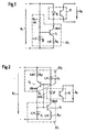
- Fig. 1 shows a known input circuit comprising an opto-coupler O and a current source ST1.
- the current source ST1 includes an ohmic resistor R V , a Zener diode S, a transistor T 1 and a series resistive resistor R S1.
- the value of the series resistor R V 10 kOhm
- that of the series resistor R S1 2.2 kOhm
- the turn-on voltage of the Zener diode S 4.7 volts.
- the transistor T 1 is, for example, an npn transistor, through which a 1.8 mAmpère current is set.
- Series resistor R V and Zener diode S are connected in series.
- Series resistor R S1 , transistor T 1 and opto-coupler O are also connected in series.
- the base of the transistor T 1 is connected to the series resistor R V and Zener diode S.
- the positive input of the input circuit is connected to the series resistor R V and the opto-coupler O, the negative input with Zener diode S and series resistor R S. Between positive and negative input is the input voltage U E.
- the input circuit is designed for an input voltage range of 10 volts to 72 volts. Such relatively high fluctuations in the input voltage occur, for example, in the railway signaling technology sector and there in an assembly for the parallel input / output.
- Low input voltages lead to a low power loss, high input voltages lead to a high power loss.
- a high power loss leads to a high self-heating of the input circuit.
- the series resistor R V generates a lot of heat, resulting in a high power consumption results and requires additional equipment for cooling to counteract overheating.
- EP 0 477 596 A2 discloses a DC blocking converter circuit disclosed.
- the circuit includes a voltage divider, one Base circuit, an oscillating circuit and an output circuit as well as for the feedback and regulation of the output voltage Comparator and an optocoupler.
- the circuit includes in particular a first current source having a first transistor, a second current source with a second transistor, an intermediate resistor and a Assembly for galvanic isolation, wherein the first transistor with the negative input of the input circuit is connected and wherein the second transistor on the one hand with the positive input of the Input circuit and the other with the base of the second transistor connected is.
- DE 3432567 C1 is a circuit arrangement for Short circuit monitoring revealed. It will come in series with the Consumer switched first transistor and one of it Basic voltage divider ratio changing, with its base with the Realized collector of the first transistor connected second transistor.
- an input circuit which is a current source includes, which has a current limiting resistor with is connected to an optocoupler.
- the object of the invention is a power-optimized input circuit provide.
- Fig. 1 Compared with the prior art of Fig. 1 can significantly more Inputs are realized, which processes more information can be.
- the power dissipation e.g. to the Factor 11, may e.g. 11 times the number of inputs can be realized.
- the power loss (heat generation) at constant Number of inputs can be reduced by a factor of 11.
- Fig. 2 shows a schematic representation of an inventive Input circuit.
- the input circuit according to the invention includes two current sources ST1, ST2, a device for electrical isolation as well as an ohmic intermediate resistor R Z.
- the component for galvanic isolation is designed as an opto-coupler O. At the output of the opto-coupler O is the output voltage U A of the input circuit.
- the arrangement of the two current sources ST1, ST2 may be referred to as antiserial.
- Intermediate resistor (R Z ) and opto-coupler (O) are each connected between the two current sources (ST 1 , ST 2 ).
- Current source ST 1 includes transistor T 1 , Zener diode S 1 and ohmic series resistance R S1 .
- Current source ST 2 includes transistor T 2 , Zener diode S 2 and ohmic series resistance R S2 .
- the transistor T 1 is, for example, an npn transistor, through which a 1.8 mAmpère current is set.
- the transistor T 2 is, for example, a pnp transistor, through which a 0.59 mAmpère current is set.
- the value of the intermediate resistance R Z is for example 220 kOhm.
- the power loss P at the second current source ST 2 is a value of 3.1 mWatt for an input voltage of 10 volts and a value of 39 mWatt for an input voltage of 72 volts.
- the power loss at the input voltage 72 volts is more than a factor of 11 below the power loss in the prior art input circuit in Fig. 1.
- a current source includes a transistor, a Zener diode and a resistor.
- the power source can also a self-conducting field effect transistor with or without resistance exhibit.
Landscapes
- Physics & Mathematics (AREA)
- Engineering & Computer Science (AREA)
- Nonlinear Science (AREA)
- Electromagnetism (AREA)
- General Physics & Mathematics (AREA)
- Radar, Positioning & Navigation (AREA)
- Automation & Control Theory (AREA)
- Amplifiers (AREA)
- Direct Current Feeding And Distribution (AREA)
- Dc-Dc Converters (AREA)
- Electronic Switches (AREA)
Description
Claims (4)
- Eingangsschaltung beinhaltend eine erste Stromquelle (ST1) mit einem ersten Transistor (T1), eine zweite Stromquelle (ST2) mit einem zweiten Transistor (T2), einen Zwischenwiderstand (RZ) und eine Baugruppe zur galvanischen Trennung, wobei der erste Transistor (T1) mit dem negativen Eingang der Eingangsschaltung verbunden ist und wobei der zweite Transistor (T2) zum einen mit dem positiven Eingang der Eingangsschaltung und zum anderen mit der Basis des zweiten Transistors (T2) verbunden ist, dadurch gekennzeichnet, dass der Zwischenwiderstand direkt (RZ) zwischen die Basis des ersten Transistors (T1) und die Basis des zweiten Transistors (T2) geschaltet ist, und dass die Baugruppe zur galvanischen Trennung direkt zwischen die Basis des zweiten Transistors (T2) und den ersten Transistor (T1) geschaltet ist.
- Eingangsschaltung gemäß Anspruch 1, dadurch gekennzeichnet, dass jede Stromquelle (ST1; ST2) zusätzlich einen Widerstand (RS1; RS2) und eine Zener-Diode (S1; S2) aufweist.
- Eingangsschaltung gemäß Anspruch 2, dadurch gekennzeichnet, dass Widerstand (RS1) und Transistor (T1) der ersten Stromquelle (ST1), die Baugruppe zur galvanischen Trennung und die Zener-Diode (S2) der zweiten Stromquelle (ST2) in Reihe geschaltet sind, dass die Zener-Diode (S1) der ersten Stromquelle (ST1), und der Transistor (T2) und der Widerstand (RS2) der zweiten Stromquelle (ST2) in Reihe geschaltet sind, dass die Basis des Transistors (T1) der ersten Stromquelle (ST1) mit dem Zwischenwiderstand (RZ), dem Transistor (T2) der zweiten Stromquelle (ST2) sowie der Zener-Diode (S1) der ersten Stromquelle (ST1) verbunden ist, und dass die Basis des Transistors (T2) der zweiten Stromquelle (ST2) mit dem Zwischenwiderstand (RZ), der Zener-Diode (S2) der zweiten Stromquelle (ST2) und der Baugruppe zur galvanischen Trennung verbunden ist.
- Eingangsschaltung gemäß Anspruch 1, dadurch gekennzeichnet, dass die Baugruppe zur galvanischen Trennung als Opto-Koppler (O) ausgeführt ist.
Applications Claiming Priority (2)
| Application Number | Priority Date | Filing Date | Title |
|---|---|---|---|
| DE10125283 | 2001-05-23 | ||
| DE10125283A DE10125283A1 (de) | 2001-05-23 | 2001-05-23 | Leistungsoptimierte Eingansschaltung |
Publications (2)
| Publication Number | Publication Date |
|---|---|
| EP1261120A1 EP1261120A1 (de) | 2002-11-27 |
| EP1261120B1 true EP1261120B1 (de) | 2004-12-01 |
Family
ID=7685963
Family Applications (1)
| Application Number | Title | Priority Date | Filing Date |
|---|---|---|---|
| EP02360135A Expired - Lifetime EP1261120B1 (de) | 2001-05-23 | 2002-04-29 | Leistungsoptimierte Eingangsschaltung |
Country Status (3)
| Country | Link |
|---|---|
| EP (1) | EP1261120B1 (de) |
| AT (1) | ATE284087T1 (de) |
| DE (2) | DE10125283A1 (de) |
Families Citing this family (1)
| Publication number | Priority date | Publication date | Assignee | Title |
|---|---|---|---|---|
| DE102017131200B4 (de) * | 2017-12-22 | 2019-09-05 | Pilz Gmbh & Co. Kg | Digitale Eingangsschaltung zum Empfangen digitaler Eingangssignale eines Signalgebers |
Family Cites Families (5)
| Publication number | Priority date | Publication date | Assignee | Title |
|---|---|---|---|---|
| DE3150176C2 (de) * | 1981-12-18 | 1984-05-30 | Licentia Patent-Verwaltungs-Gmbh, 6000 Frankfurt | Elektronischer Konstantstromgeber für Hochspannungsgeräte |
| DE3432567C1 (de) * | 1984-09-05 | 1985-12-05 | Standard Elektrik Lorenz Ag, 7000 Stuttgart | Schaltungsanordnung zur Kurzschlußüberwachung |
| DE3916832A1 (de) * | 1989-05-19 | 1990-11-22 | Siemens Ag | Schaltungsanordnung zm potentialfreien erfassen von binaeren elektrischen signalen |
| AT399626B (de) * | 1990-09-26 | 1995-06-26 | Siemens Ag Oesterreich | Sperrwandlerschaltung |
| US6043703A (en) * | 1997-07-30 | 2000-03-28 | Allen-Bradley Company, Llc | Low power active input circuit |
-
2001
- 2001-05-23 DE DE10125283A patent/DE10125283A1/de not_active Withdrawn
-
2002
- 2002-04-29 AT AT02360135T patent/ATE284087T1/de not_active IP Right Cessation
- 2002-04-29 DE DE50201652T patent/DE50201652D1/de not_active Expired - Lifetime
- 2002-04-29 EP EP02360135A patent/EP1261120B1/de not_active Expired - Lifetime
Also Published As
| Publication number | Publication date |
|---|---|
| DE10125283A1 (de) | 2002-11-28 |
| EP1261120A1 (de) | 2002-11-27 |
| DE50201652D1 (de) | 2005-01-05 |
| ATE284087T1 (de) | 2004-12-15 |
Similar Documents
| Publication | Publication Date | Title |
|---|---|---|
| DE69505633T2 (de) | Gleichrichterbrückenschaltung mit aktiven schaltern und einer aktiven steuerschaltung | |
| DE3632746C2 (de) | Schaltungsanordnung zur Erzeugung einer Wechselspannung | |
| DE3907410C1 (de) | ||
| DE68913277T2 (de) | Schutz für Leistungswandler gegen Spannungsspitzen. | |
| DE102007060219A1 (de) | Gleichrichterschaltung | |
| DE10392856T5 (de) | Aktiver Emi Filter | |
| DE102013107941A1 (de) | Stromwandler mit parallel betätigten Schaltelementen | |
| EP1110035A2 (de) | Verfahren und vorrichtung zur steuerung eines abschaltbaren stromrichterventils mit der reihenschaltzahl zwei oder grösser | |
| DE102014107815A1 (de) | System und Verfahren zum Ansteuern von Transistoren | |
| DE102019001761A1 (de) | Motorantriebsvorrichtung | |
| DE3009506A1 (de) | Gleichspannungswandler | |
| WO2002023704A1 (de) | Schaltungsanordnung zur energieversorgung für eine ansteuerschaltung eines leistungshalbleiterschalters und verfahren zur bereitstellung der ansteuerenergie für einen leistungshalbleiterschalter | |
| DE10125283A1 (de) | Leistungsoptimierte Eingansschaltung | |
| DE102019118341B3 (de) | Linearlichteinheit, Lichtquellenmodul für eine solche Linearlichteinheit sowie Verfahren zum Betreiben einer solchen Linearlichteinheit | |
| DE10314842A1 (de) | Stromerfassungsschaltung für einen DC/DC-Wandler | |
| DE10339470A1 (de) | Steuerschaltung für ein Schaltnetzteil | |
| US20020017942A1 (en) | Voltage division method for protection a gainst load dump conditions | |
| DE112020005368T5 (de) | Halbleitervorrichtung | |
| DE60212085T2 (de) | Schaltnetzteil mit verringerter oberwellenbelastung des netzes | |
| DE2425579C3 (de) | Schaltungsanordnung für den Anschluß eines mit einem elektronischen Decoder versehenen Rundsteuerempfängers an ein Wechselspannungsnetz | |
| DE102020117172A1 (de) | Elektrische Schaltungsanordnung, Leistungsmodul, Wechselrichterschaltung und Kraftfahrzeug | |
| DE102025145349B3 (de) | Verfahren zum Betreiben eines Energieumformers, Energieumformer zum elektrischen Koppeln eines Gleichspannungsbordnetzes mit einer elektrischen Maschine sowie Kraftfahrzeug | |
| DE4428674A1 (de) | Verfahren und Vorrichtung zur Steuerung des Abschaltvorgangs eines spannungsgesteuerten, abschaltbaren Leistungshalbleiter-Schalters | |
| DE102018219328B4 (de) | Erkennen eines Drahtbruchfehlers in einem Stromkreis | |
| DE102004020792B4 (de) | Elektrischer Schaltwandler mit hoher Eingangsspannung |
Legal Events
| Date | Code | Title | Description |
|---|---|---|---|
| PUAI | Public reference made under article 153(3) epc to a published international application that has entered the european phase |
Free format text: ORIGINAL CODE: 0009012 |
|
| 17P | Request for examination filed |
Effective date: 20021001 |
|
| AK | Designated contracting states |
Kind code of ref document: A1 Designated state(s): AT BE CH CY DE DK ES FI FR GB GR IE IT LI LU MC NL PT SE TR |
|
| AX | Request for extension of the european patent |
Free format text: AL;LT;LV;MK;RO;SI |
|
| 17Q | First examination report despatched |
Effective date: 20030203 |
|
| AKX | Designation fees paid |
Designated state(s): AT BE CH CY DE DK ES FI FR GB GR IE IT LI LU MC NL PT SE TR |
|
| GRAP | Despatch of communication of intention to grant a patent |
Free format text: ORIGINAL CODE: EPIDOSNIGR1 |
|
| GRAS | Grant fee paid |
Free format text: ORIGINAL CODE: EPIDOSNIGR3 |
|
| GRAA | (expected) grant |
Free format text: ORIGINAL CODE: 0009210 |
|
| AK | Designated contracting states |
Kind code of ref document: B1 Designated state(s): AT BE CH CY DE DK ES FI FR GB GR IE IT LI LU MC NL PT SE TR |
|
| PG25 | Lapsed in a contracting state [announced via postgrant information from national office to epo] |
Ref country code: IE Free format text: LAPSE BECAUSE OF FAILURE TO SUBMIT A TRANSLATION OF THE DESCRIPTION OR TO PAY THE FEE WITHIN THE PRESCRIBED TIME-LIMIT Effective date: 20041201 Ref country code: FI Free format text: LAPSE BECAUSE OF FAILURE TO SUBMIT A TRANSLATION OF THE DESCRIPTION OR TO PAY THE FEE WITHIN THE PRESCRIBED TIME-LIMIT Effective date: 20041201 Ref country code: NL Free format text: LAPSE BECAUSE OF FAILURE TO SUBMIT A TRANSLATION OF THE DESCRIPTION OR TO PAY THE FEE WITHIN THE PRESCRIBED TIME-LIMIT Effective date: 20041201 Ref country code: TR Free format text: LAPSE BECAUSE OF FAILURE TO SUBMIT A TRANSLATION OF THE DESCRIPTION OR TO PAY THE FEE WITHIN THE PRESCRIBED TIME-LIMIT Effective date: 20041201 |
|
| REG | Reference to a national code |
Ref country code: GB Ref legal event code: FG4D Free format text: NOT ENGLISH |
|
| REG | Reference to a national code |
Ref country code: CH Ref legal event code: EP |
|
| GBT | Gb: translation of ep patent filed (gb section 77(6)(a)/1977) |
Effective date: 20041201 |
|
| REG | Reference to a national code |
Ref country code: IE Ref legal event code: FG4D Free format text: GERMAN |
|
| REF | Corresponds to: |
Ref document number: 50201652 Country of ref document: DE Date of ref document: 20050105 Kind code of ref document: P |
|
| PG25 | Lapsed in a contracting state [announced via postgrant information from national office to epo] |
Ref country code: SE Free format text: LAPSE BECAUSE OF FAILURE TO SUBMIT A TRANSLATION OF THE DESCRIPTION OR TO PAY THE FEE WITHIN THE PRESCRIBED TIME-LIMIT Effective date: 20050301 Ref country code: DK Free format text: LAPSE BECAUSE OF FAILURE TO SUBMIT A TRANSLATION OF THE DESCRIPTION OR TO PAY THE FEE WITHIN THE PRESCRIBED TIME-LIMIT Effective date: 20050301 Ref country code: GR Free format text: LAPSE BECAUSE OF FAILURE TO SUBMIT A TRANSLATION OF THE DESCRIPTION OR TO PAY THE FEE WITHIN THE PRESCRIBED TIME-LIMIT Effective date: 20050301 |
|
| PG25 | Lapsed in a contracting state [announced via postgrant information from national office to epo] |
Ref country code: ES Free format text: LAPSE BECAUSE OF FAILURE TO SUBMIT A TRANSLATION OF THE DESCRIPTION OR TO PAY THE FEE WITHIN THE PRESCRIBED TIME-LIMIT Effective date: 20050312 |
|
| PG25 | Lapsed in a contracting state [announced via postgrant information from national office to epo] |
Ref country code: AT Free format text: LAPSE BECAUSE OF NON-PAYMENT OF DUE FEES Effective date: 20050429 Ref country code: LU Free format text: LAPSE BECAUSE OF NON-PAYMENT OF DUE FEES Effective date: 20050429 Ref country code: CY Free format text: LAPSE BECAUSE OF FAILURE TO SUBMIT A TRANSLATION OF THE DESCRIPTION OR TO PAY THE FEE WITHIN THE PRESCRIBED TIME-LIMIT Effective date: 20050429 |
|
| PG25 | Lapsed in a contracting state [announced via postgrant information from national office to epo] |
Ref country code: MC Free format text: LAPSE BECAUSE OF NON-PAYMENT OF DUE FEES Effective date: 20050430 Ref country code: BE Free format text: LAPSE BECAUSE OF NON-PAYMENT OF DUE FEES Effective date: 20050430 |
|
| NLV1 | Nl: lapsed or annulled due to failure to fulfill the requirements of art. 29p and 29m of the patents act | ||
| REG | Reference to a national code |
Ref country code: IE Ref legal event code: FD4D |
|
| PLBE | No opposition filed within time limit |
Free format text: ORIGINAL CODE: 0009261 |
|
| STAA | Information on the status of an ep patent application or granted ep patent |
Free format text: STATUS: NO OPPOSITION FILED WITHIN TIME LIMIT |
|
| BERE | Be: lapsed |
Owner name: ALCATEL Effective date: 20050430 |
|
| 26N | No opposition filed |
Effective date: 20050902 |
|
| ET | Fr: translation filed | ||
| PG25 | Lapsed in a contracting state [announced via postgrant information from national office to epo] |
Ref country code: CH Free format text: LAPSE BECAUSE OF NON-PAYMENT OF DUE FEES Effective date: 20060430 Ref country code: LI Free format text: LAPSE BECAUSE OF NON-PAYMENT OF DUE FEES Effective date: 20060430 |
|
| REG | Reference to a national code |
Ref country code: CH Ref legal event code: PL |
|
| BERE | Be: lapsed |
Owner name: *ALCATEL Effective date: 20050430 |
|
| PG25 | Lapsed in a contracting state [announced via postgrant information from national office to epo] |
Ref country code: PT Free format text: LAPSE BECAUSE OF NON-PAYMENT OF DUE FEES Effective date: 20050501 |
|
| REG | Reference to a national code |
Ref country code: FR Ref legal event code: PLFP Year of fee payment: 15 |
|
| REG | Reference to a national code |
Ref country code: FR Ref legal event code: PLFP Year of fee payment: 16 |
|
| REG | Reference to a national code |
Ref country code: FR Ref legal event code: PLFP Year of fee payment: 17 |
|
| PGFP | Annual fee paid to national office [announced via postgrant information from national office to epo] |
Ref country code: FR Payment date: 20200414 Year of fee payment: 19 Ref country code: DE Payment date: 20200415 Year of fee payment: 19 |
|
| PGFP | Annual fee paid to national office [announced via postgrant information from national office to epo] |
Ref country code: IT Payment date: 20200414 Year of fee payment: 19 Ref country code: GB Payment date: 20200411 Year of fee payment: 19 |
|
| REG | Reference to a national code |
Ref country code: DE Ref legal event code: R119 Ref document number: 50201652 Country of ref document: DE |
|
| GBPC | Gb: european patent ceased through non-payment of renewal fee |
Effective date: 20210429 |
|
| PG25 | Lapsed in a contracting state [announced via postgrant information from national office to epo] |
Ref country code: DE Free format text: LAPSE BECAUSE OF NON-PAYMENT OF DUE FEES Effective date: 20211103 Ref country code: GB Free format text: LAPSE BECAUSE OF NON-PAYMENT OF DUE FEES Effective date: 20210429 Ref country code: FR Free format text: LAPSE BECAUSE OF NON-PAYMENT OF DUE FEES Effective date: 20210430 |
|
| PG25 | Lapsed in a contracting state [announced via postgrant information from national office to epo] |
Ref country code: IT Free format text: LAPSE BECAUSE OF NON-PAYMENT OF DUE FEES Effective date: 20200429 |
|
| PG25 | Lapsed in a contracting state [announced via postgrant information from national office to epo] |
Ref country code: IT Free format text: LAPSE BECAUSE OF NON-PAYMENT OF DUE FEES Effective date: 20210429 |