EP1258911A2 - Method of using titanium doped aluminium oxide for passivation of ferroelectric materials and devices including the same - Google Patents
Method of using titanium doped aluminium oxide for passivation of ferroelectric materials and devices including the same Download PDFInfo
- Publication number
- EP1258911A2 EP1258911A2 EP02006938A EP02006938A EP1258911A2 EP 1258911 A2 EP1258911 A2 EP 1258911A2 EP 02006938 A EP02006938 A EP 02006938A EP 02006938 A EP02006938 A EP 02006938A EP 1258911 A2 EP1258911 A2 EP 1258911A2
- Authority
- EP
- European Patent Office
- Prior art keywords
- titanium
- oxygen
- aluminum
- range
- argon
- Prior art date
- Legal status (The legal status is an assumption and is not a legal conclusion. Google has not performed a legal analysis and makes no representation as to the accuracy of the status listed.)
- Withdrawn
Links
Images



Classifications
-
- H—ELECTRICITY
- H10—SEMICONDUCTOR DEVICES; ELECTRIC SOLID-STATE DEVICES NOT OTHERWISE PROVIDED FOR
- H10D—INORGANIC ELECTRIC SEMICONDUCTOR DEVICES
- H10D84/00—Integrated devices formed in or on semiconductor substrates that comprise only semiconducting layers, e.g. on Si wafers or on GaAs-on-Si wafers
- H10D84/80—Integrated devices formed in or on semiconductor substrates that comprise only semiconducting layers, e.g. on Si wafers or on GaAs-on-Si wafers characterised by the integration of at least one component covered by groups H10D12/00 or H10D30/00, e.g. integration of IGFETs
-
- H—ELECTRICITY
- H10—SEMICONDUCTOR DEVICES; ELECTRIC SOLID-STATE DEVICES NOT OTHERWISE PROVIDED FOR
- H10D—INORGANIC ELECTRIC SEMICONDUCTOR DEVICES
- H10D1/00—Resistors, capacitors or inductors
- H10D1/60—Capacitors
- H10D1/68—Capacitors having no potential barriers
- H10D1/682—Capacitors having no potential barriers having dielectrics comprising perovskite structures
-
- H—ELECTRICITY
- H10—SEMICONDUCTOR DEVICES; ELECTRIC SOLID-STATE DEVICES NOT OTHERWISE PROVIDED FOR
- H10N—ELECTRIC SOLID-STATE DEVICES NOT OTHERWISE PROVIDED FOR
- H10N30/00—Piezoelectric or electrostrictive devices
- H10N30/80—Constructional details
- H10N30/88—Mounts; Supports; Enclosures; Casings
- H10N30/883—Additional insulation means preventing electrical, physical or chemical damage, e.g. protective coatings
-
- H—ELECTRICITY
- H10—SEMICONDUCTOR DEVICES; ELECTRIC SOLID-STATE DEVICES NOT OTHERWISE PROVIDED FOR
- H10P—GENERIC PROCESSES OR APPARATUS FOR THE MANUFACTURE OR TREATMENT OF DEVICES COVERED BY CLASS H10
- H10P14/00—Formation of materials, e.g. in the shape of layers or pillars
- H10P14/60—Formation of materials, e.g. in the shape of layers or pillars of insulating materials
- H10P14/63—Formation of materials, e.g. in the shape of layers or pillars of insulating materials characterised by the formation processes
- H10P14/6326—Deposition processes
- H10P14/6328—Deposition from the gas or vapour phase
- H10P14/6329—Deposition from the gas or vapour phase using physical ablation of a target, e.g. physical vapour deposition or pulsed laser deposition
-
- H—ELECTRICITY
- H10—SEMICONDUCTOR DEVICES; ELECTRIC SOLID-STATE DEVICES NOT OTHERWISE PROVIDED FOR
- H10P—GENERIC PROCESSES OR APPARATUS FOR THE MANUFACTURE OR TREATMENT OF DEVICES COVERED BY CLASS H10
- H10P14/00—Formation of materials, e.g. in the shape of layers or pillars
- H10P14/60—Formation of materials, e.g. in the shape of layers or pillars of insulating materials
- H10P14/65—Formation of materials, e.g. in the shape of layers or pillars of insulating materials characterised by treatments performed before or after the formation of the materials
- H10P14/6516—Formation of materials, e.g. in the shape of layers or pillars of insulating materials characterised by treatments performed before or after the formation of the materials of treatments performed after formation of the materials
- H10P14/6529—Formation of materials, e.g. in the shape of layers or pillars of insulating materials characterised by treatments performed before or after the formation of the materials of treatments performed after formation of the materials by exposure to a gas or vapour
-
- H—ELECTRICITY
- H10—SEMICONDUCTOR DEVICES; ELECTRIC SOLID-STATE DEVICES NOT OTHERWISE PROVIDED FOR
- H10P—GENERIC PROCESSES OR APPARATUS FOR THE MANUFACTURE OR TREATMENT OF DEVICES COVERED BY CLASS H10
- H10P14/00—Formation of materials, e.g. in the shape of layers or pillars
- H10P14/60—Formation of materials, e.g. in the shape of layers or pillars of insulating materials
- H10P14/65—Formation of materials, e.g. in the shape of layers or pillars of insulating materials characterised by treatments performed before or after the formation of the materials
- H10P14/6516—Formation of materials, e.g. in the shape of layers or pillars of insulating materials characterised by treatments performed before or after the formation of the materials of treatments performed after formation of the materials
- H10P14/6529—Formation of materials, e.g. in the shape of layers or pillars of insulating materials characterised by treatments performed before or after the formation of the materials of treatments performed after formation of the materials by exposure to a gas or vapour
- H10P14/6532—Formation of materials, e.g. in the shape of layers or pillars of insulating materials characterised by treatments performed before or after the formation of the materials of treatments performed after formation of the materials by exposure to a gas or vapour by exposure to a plasma
-
- H—ELECTRICITY
- H10—SEMICONDUCTOR DEVICES; ELECTRIC SOLID-STATE DEVICES NOT OTHERWISE PROVIDED FOR
- H10P—GENERIC PROCESSES OR APPARATUS FOR THE MANUFACTURE OR TREATMENT OF DEVICES COVERED BY CLASS H10
- H10P14/00—Formation of materials, e.g. in the shape of layers or pillars
- H10P14/60—Formation of materials, e.g. in the shape of layers or pillars of insulating materials
- H10P14/69—Inorganic materials
- H10P14/692—Inorganic materials composed of oxides, glassy oxides or oxide-based glasses
- H10P14/6938—Inorganic materials composed of oxides, glassy oxides or oxide-based glasses the material containing at least one metal element, e.g. metal oxides, metal oxynitrides or metal oxycarbides
- H10P14/6939—Inorganic materials composed of oxides, glassy oxides or oxide-based glasses the material containing at least one metal element, e.g. metal oxides, metal oxynitrides or metal oxycarbides characterised by the metal
- H10P14/69391—Inorganic materials composed of oxides, glassy oxides or oxide-based glasses the material containing at least one metal element, e.g. metal oxides, metal oxynitrides or metal oxycarbides characterised by the metal the material containing aluminium, e.g. Al2O3
-
- H—ELECTRICITY
- H10—SEMICONDUCTOR DEVICES; ELECTRIC SOLID-STATE DEVICES NOT OTHERWISE PROVIDED FOR
- H10P—GENERIC PROCESSES OR APPARATUS FOR THE MANUFACTURE OR TREATMENT OF DEVICES COVERED BY CLASS H10
- H10P14/00—Formation of materials, e.g. in the shape of layers or pillars
- H10P14/60—Formation of materials, e.g. in the shape of layers or pillars of insulating materials
- H10P14/69—Inorganic materials
- H10P14/692—Inorganic materials composed of oxides, glassy oxides or oxide-based glasses
- H10P14/6938—Inorganic materials composed of oxides, glassy oxides or oxide-based glasses the material containing at least one metal element, e.g. metal oxides, metal oxynitrides or metal oxycarbides
- H10P14/6939—Inorganic materials composed of oxides, glassy oxides or oxide-based glasses the material containing at least one metal element, e.g. metal oxides, metal oxynitrides or metal oxycarbides characterised by the metal
- H10P14/69394—Inorganic materials composed of oxides, glassy oxides or oxide-based glasses the material containing at least one metal element, e.g. metal oxides, metal oxynitrides or metal oxycarbides characterised by the metal the material containing titanium, e.g. TiO2
-
- H—ELECTRICITY
- H10—SEMICONDUCTOR DEVICES; ELECTRIC SOLID-STATE DEVICES NOT OTHERWISE PROVIDED FOR
- H10P—GENERIC PROCESSES OR APPARATUS FOR THE MANUFACTURE OR TREATMENT OF DEVICES COVERED BY CLASS H10
- H10P14/00—Formation of materials, e.g. in the shape of layers or pillars
- H10P14/60—Formation of materials, e.g. in the shape of layers or pillars of insulating materials
- H10P14/69—Inorganic materials
- H10P14/692—Inorganic materials composed of oxides, glassy oxides or oxide-based glasses
- H10P14/6938—Inorganic materials composed of oxides, glassy oxides or oxide-based glasses the material containing at least one metal element, e.g. metal oxides, metal oxynitrides or metal oxycarbides
- H10P14/6939—Inorganic materials composed of oxides, glassy oxides or oxide-based glasses the material containing at least one metal element, e.g. metal oxides, metal oxynitrides or metal oxycarbides characterised by the metal
- H10P14/69397—Inorganic materials composed of oxides, glassy oxides or oxide-based glasses the material containing at least one metal element, e.g. metal oxides, metal oxynitrides or metal oxycarbides characterised by the metal the material containing two or more metal elements
-
- H—ELECTRICITY
- H10—SEMICONDUCTOR DEVICES; ELECTRIC SOLID-STATE DEVICES NOT OTHERWISE PROVIDED FOR
- H10P—GENERIC PROCESSES OR APPARATUS FOR THE MANUFACTURE OR TREATMENT OF DEVICES COVERED BY CLASS H10
- H10P72/00—Handling or holding of wafers, substrates or devices during manufacture or treatment thereof
- H10P72/04—Apparatus for manufacture or treatment
- H10P72/0402—Apparatus for fluid treatment
- H10P72/0418—Apparatus for fluid treatment for etching
- H10P72/0422—Apparatus for fluid treatment for etching for wet etching
- H10P72/0426—Apparatus for fluid treatment for etching for wet etching with the semiconductor substrates being dipped in baths or vessels
Definitions
- This invention relates to a method of using titanium-doped aluminum oxide for passivation of ferroelectric materials and devices including the same and, more particularly, to a method of using titanium-doped aluminum oxide for passivation of ferroelectric materials and devices including the same in FeRAM and DRAM applications.
- FeRAM Ferroelectric random access memory
- DRAM dynamic random access memory
- FeRAM structures therefore, may be widely used in the future, if these structures can be successfully integrated into real working devices.
- ferroelectric materials into real devices, however, has resulted in many difficulties.
- the ferroelectric material is usually sandwiched between a bottom and a top electrode in order to polarize the ferroelectric material. Passivation of the ferroelectric material, therefore, usually requires passivation of the metal/ferroelectric/metal (MFM) structure.
- MFM metal/ferroelectric/metal
- Platinum (Pt) has been widely used as the material for the top and bottom electrodes in ferroelectric material based devices such as capacitors.
- the major drawback of using Platinum as a top electrode is its catalytic nature with Hydrogen.
- Titanium Dioxide has been shown to have passivation properties toward gas annealing in a forming gas ambient
- the pressure may range from only a few mTorr to 76 Torr or higher.
- a very thin layer of Al 2 O 3 has also been shown to be effective in protecting ferroelectric capacitors during forming gas annealing.
- MFM structures with TiO 2 passivation layers have been shown to be more susceptible to leakage after the forming gas annealing step.
- Al 2 O 3 layers deposited by physical vapor deposition (PVD) show large stress factors and are difficult to oxidize.
- PVD physical vapor deposition
- This invention comprises a passivation material that can be used in nonvolatile memory devices, DRAMs, capacitors, pyroelectric infrared sensors, optical displays, optical switches, piezoelectric transducers, and surface acoustic wave devices. More particularly, the invention comprises a titanium-doped aluminum oxide layer for passivation of ferroelectric materials and a method of manufacturing the same and, more particularly, to a titanium-doped aluminum oxide layer for passivation of ferroelectric materials that has reduced stress and improved passivation properties, and that is easy to deposit and be oxidized.
- the invention comprises an integrated circuit device comprising a ferroelectric material positioned between first and second metal electrodes; and a passivation layer positioned on said first electrode, said passivation layer comprising Titanium doped Aluminum Oxide.
- the invention also comprises a method of manufacturing an integrated circuit device including a ferroelectric structure having a passivation layer, comprising the steps of: providing a deposition chamber, providing in said deposition chamber a ferroelectric structure including a ferroelectric material positioned between top and bottom electrodes; providing Aluminum and Titanium targets in said deposition chamber, and sputtering said Aluminum and said Titanium targets so as to form a Titanium doped Aluminum Oxide passivation layer on said top electrode.
- an object of the invention is to provide a passivation material that can be used in nonvolatile memory devices, DRAMs, capacitors, pyroelectric infrared sensors, optical displays, optical switches, piezoelectric transducers, or surface acoustic wave devices.
- Another object of the invention is to provide a titanium-doped aluminum oxide layer for passivation of ferroelectric materials and a method of manufacturing the same.
- a further object of the invention is to provide a titanium-doped aluminum oxide layer for passivation of ferroelectric materials that has reduced stress and improved passivation properties
- Still a further object of the invention is to provide a titanium-doped aluminum oxide layer for passivation of ferroelectric materials that is easy to deposit and be oxidized.
- FIG. 1 is a photograph of a damaged prior art MFM structure having an Al 2 O 3 passivation layer after forming gas annealing.
- FIG. 2 is a photograph of a damaged prior art MFM structure having a TiO 2 passivation layer after annealing in an oxygen ambient
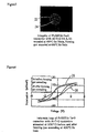
- FIG. 3 is a photograph of an undamaged MFM structure having a Titanium doped Aluminum Oxide passivation layer of the present invention after forming gas annealing.
- FIG. 4 is a hysteresis loop of the MFM structure of FIG. 3.
- FIG. 5 is a photograph of a single transistor with a Titanium doped Aluminum Oxide passivation layer after forming gas annealing.
- FIG. 6 is a hysteresis loop of the MFM structure of FIG. 5.
- FIG. 7 is a photograph of a single transistor without a Titanium doped Aluminum Oxide passivation layer after forming gas annealing.
- FIG. 8 is a graph of an X-ray Diffraction spectrum of a Titanium doped Aluminum Oxide passivation layer sputtered in pure Argon and annealed at different conditions.
- FIG. 9 is a graph of an X-ray Diffraction spectrum of a Titanium doped Aluminum Oxide passivation layer sputtered in a mix of Argon and Oxygen, and annealed at different conditions.
- FIG. 10 is a flowchart of the method of the present invention.
- FIG. 1 shows a photograph of a damaged prior art device 10 comprising a capacitor including an AlO x passivation layer 12, namely Al 2 O 3 , on a metal/ferroelectric/metal (MFM) structure 14.
- MFM structure comprises a Platinum (Pt) top electrode on a Strontium Bismuth Tantalate (SBT or SrBi 2 Ta 2 O 9 ) ferroelectric material, which is on an Iridium Tantalum Oxygen (Ir-Ta-O) bottom electrode.
- the AlO x passivation layer was deposited by sputtering Aluminum in an O 2 atmosphere, or ambient, and then subjecting the structure to rapid thermal processing (RTP) in an Oxygen ambient at 500 degrees Celsius for thirty minutes.
- RTP rapid thermal processing
- the structure was then subjected to forming gas annealing at 400 degrees Celsius for five minutes in a forming gas ambient.
- the forming gas normally comprises nitrogen and hydrogen with hydrogen present in a range of 3% to 5%, with nitrogen comprising, essentially, the remainder of the gas composition.
- the hydrogen may be present in the forming gas in a range of anywhere from 1% to 15%.
- the pressure of the forming gas ambient may be anywhere from several mTorr to 76 Torr or more.
- the AlOx layer formed has a thickness of approximately 325 Angstroms (325 A).
- the passivation layer formed on the MFM structure shows Hydrogen damage due to the annealing process. In particular, during the annealing step most of the top electrode peeled from the ferroelectric layer and the capacitor shorted. Accordingly, the AlO x passivation layer is unsatisfactory for use in real devices.
- FIG. 2 is a photograph of a damaged prior art device 16 comprising a capacitor having a TiO 2 passivation layer 18 on a metal/ferroelectric/metal (MFM) structure 20.
- MFM structure 20 comprises a Platinum top electrode on a Strontium Bismuth Tantalate (SBT or SrBi 2 Ta 2 O 9 ) ferroelectric material, on an Iridium Tantalum Oxygen bottom electrode.
- SBT or SrBi 2 Ta 2 O 9 Strontium Bismuth Tantalate
- the TiO 2 passivation layer was deposited by reactive sputtering a Titanium target in an Oxygen atmosphere. The thickness of the deposited TiO 2 layer is approximately 800 Angstroms.
- the structure was then subjected to an annealing process in an Oxygen atmosphere at 500 degrees Celsius for thirty minutes.
- the structure having the TiO 2 passivation layer appeared to have undergone even more stress than the structure having the AlO x passivation layer of FIG. 1. After the annealing step, it can be seen that most of the top electrode of structure 20 has peeled off the ferroelectric material. Accordingly, the TiO 2 passivation layer is unsatisfactory for use in real devices.
- FIG. 3 is a photograph of an undamaged MFM structure 22 having the Titanium doped Aluminum Oxide passivation layer 24 of the present invention.
- MFM structure 22 comprises a Platinum top electrode on a Strontium Bismuth Tantalate (SBT or SrBi 2 Ta 2 O 9 ) ferroelectric material, on an Iridium Tanalum Oxygen bottom electrode.
- SBT or SrBi 2 Ta 2 O 9 Strontium Bismuth Tantalate
- the Titanium doped Aluminum Oxide (Al-Ti-O) passivation layer 24 was deposited by co-sputtering Titanium and Aluminum targets in an O 2 atmosphere followed by an in-situ plasma treatment, the details of which are set forth below.
- the film was annealed in an oxygen ambient at 500 °C for thirty minutes. By oxygen ambient Applicants mean an oxygen rich atmosphere.
- the oxygen ambient may comprise an atmosphere having an oxygen content of as little as 20% or more.
- An oxygen content of 50% or more is preferred and an oxygen content of 99% or more is ideal.
- the structure was then subjected to an annealing step at 400 degrees Celsius for five minutes in a forming gas ambient to test the device.
- the Al-Ti-O passivation layer formed on the MFM has a thickness of approximately 226 Angstroms (226 A).
- the passivation layer shows no Hydrogen damage due to the annealing process. In particular, during the annealing step the top electrode did not peel from the ferroelectric layer and the capacitor did not short. Accordingly, the Al-Ti-O passivation layer of the present invention is satisfactory for use in real devices.
- FIG. 4 is a hysteresis loop of the MFM structure of FIG. 3.
- Hysteresis loop 26 shows the polarization versus voltage before annealing of the MFM device of FIG. 3.
- Heteresis loop 28 shows the remnant polarization (Pr) of MFM structure 22 of FIG. 3 after forming gas annealing of the metal-ferroelctric-metal (MFM) structure at 400 degrees Celsius for five minutes.
- the MFM structure is shown to have maintained good integrity and its remnant polarization remains almost the same after the annealing step.
- the remnant polarization of the MFM structure after forming gas annealing is within 20% of the remnant polarization of the structure before the annealing step.
- the Ti-Al-O passivation layer of the present invention is an improvement over the passivation layers of the prior art shown in FIGS. 1 and 2 and can be used in real working devices.
- FIG. 5 is a photograph of a single transistor 30 with a Titanium doped Aluminum Oxide passivation layer 32.
- the passivation layer was formed by co-sputtering Titanium and Aluminum targets in an O 2 ambient and then annealing in an oxygen ambient at 500 degrees Celsius for thirty minutes.
- the manufacturing steps include inter-layer dielectric (ILD) layer deposition, contact etch, metallization and a final annealing step at 400 degrees Celsius for five minutes in a forming gas ambient to test the structure.
- the Al-Ti-O layer formed has a thickness of approximately 350 Angstroms (350 A).
- the MFM structure on the SBT single transistor shows no Hydrogen damage due to the annealing process. In particular, during the annealing step the top electrode did not peel from the ferroelectric layer and the capacitor did not short. Accordingly, the Al-Ti-O passivation layer single transistor performed satisfactorily.
- FIG. 6 is a hysteresis loop of the MFM structure of FIG. 5 after metallization and after the annealing step.
- loop 34 is a hysteresis loop of the SBT film buried in the single transistor after the metallization step and before the forming gas annealing step.
- Loop 36 is a hysteresis loop of the SBT film buried in the single transistor after the forming gas annealing step at 400 degrees Celsius for five minutes in a forming gas ambient.
- the remnant polarization 36 of the transistor does not substantially change after the annealing step, and is with 20 percent of the remnant polarization of hysteresis loop 34.
- FIG. 7 is a photograph of a single transistor 3 8 without a Titanium doped Aluminum Oxide passivation layer. As can be seen in the photograph, the transistor without the Titanium doped Aluminum Oxide passivation layer has failed. Accordingly, no hysteresis loop is shown for the failed transistor.
- FIG. 8 is a graph of the X-ray Diffraction spectrum of a Titanium doped Aluminum Oxide passivation layer sputtered in pure Argon and annealed at different conditions, wherein the x-axis represents degrees (2 x theta) and the y-axis represents counts/second.
- the Ti-Al-O passivation layer including preferably a 15% or less doping of Titanium, was deposited in pure Argon. Passivation layers deposited under these conditions are shown as subjected to three annealing conditions: 500 degrees Celsius for thirty minutes (line 40); 500 degrees Celsius for fifteen minutes (line 42); and as deposited (line 44). The annealing steps took place in an Oxygen ambient for full oxidation. It can be seen from the graph that metallic Aluminum with lightly doped Titanium deposited in pure Argon is very hard to oxidize.
- FIG. 9 is a graph of the X-ray Diffraction spectrum of a Titanium doped Aluminum Oxide passivation layer sputtered in a mix of Argon and Oxygen and annealed at different conditions.
- the structure was then further annealed in an Oxygen atmosphere for full oxidation.
- Passivation layers deposited under these conditions are shown as subjected to three annealing conditions: 500 degrees Celsius for thirty minutes (line 46); 500 degrees Celsius for fifteen minutes (line 48); and as deposited (line 50).
- This phenomenon is explained in that the deposition only occurred at the very beginning of the deposition, so that the surface of the targets are oxidized and the deposition stopped after oxidization of the targets. Accordingly, this phenomenon can be used as an advantage in plasma treatment of the already deposited oxide film.
- the shutters provided at the targets are initially closed so as to allow sputtering of the targets themselves. The shutters are then opened so as to allow sputtering of the wafer.
- the shutters then remain open and the oxygen pressure is increased, so as to continue to generate an oxygen plasma.
- the oxygen partial pressure is high, the deposition of the passivation film is essentially stopped, but the oxygen plasma continues to be generated.
- the oxygen plasma can reach the surface of the already deposited Titanium doped Aluminum Oxide and further oxidize the film.
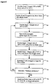
- FIG. 10 is a flowchart of the method of the present invention.
- the method comprises co-sputtering Aluminum and Titanium targets in an Oxygen environment followed by an in-situ plasma treatment and a final annealing step.
- the co-sputtering steps can be repeated multiple times until the desired thickness of the titanium doped Aluminum Oxide film is reached.
- step 60 includes providing four inch Aluminum and Titanium targets. Of course, other sized targets may be provided.
- the sputtering power on the four inch targets may range from 10W to 800W.
- the ratio of the powers on the Al and Ti targets is preferably about 10:1 to 3:1 to obtain atomic percent Ti at 1% to 30% in the Al-Ti-O film.
- Step 62 includes sputtering the surface of the MFM device, such as a Pt/SBT/Ir-Ta-O structure, in an Argon environment with the shutter closed for 30 seconds to 10 minutes.
- Step 64 includes turning on the Oxygen gas supply.
- the Argon/Oxygen ratio is between 10/1 to 10/10.
- Step 66 comprises opening the shutter on the Al and the Ti targets and then sputtering the targets for 10 seconds to five minutes.
- Step 68 includes increasing the Oxygen partial pressure so that the Ar/O 2 ratio is between approximately 10/8 to 10/20. The power is retained on both the targets to the shutter is retained open.
- Step 70 includes reducing the Oxygen partial pressure to 10/1 to 10/10, closing the shutter, and closing the Oxygen source.
- Step 72 includes sputtering the Ti and Al target surfaces in an Argon atmosphere for another 30 seconds to 10 minutes.
- Step 74 includes determining whether the thickness of the deposited Titanium doped Aluminum Oxide film (Ti doped Al 2 O 3 ) is satisfactory. The film thickness of each cycle including steps 62-72 is approximately 50 to 500 Angstroms, depending on the sputtering power and the sputtering time. If the thickness is not satisfactory, then steps 64-72 are repeated.
- Step 76 includes annealing the Ti doped Al 2 O 3 layer at a temperature in a range of 400 to 800 degrees Celsius for approximately ten seconds to one hour in an Oxygen atmosphere to fully oxidize the film.
- the method steps listed above result in a passivation layer comprised of Titanium doped Aluminum Oxide which has reduced stress compared with pure Aluminum Oxide films.
- the Titanium doped Aluminum Oxide also is easier to oxidize than pure Aluminum Oxide films.
- the inventive passivation layer allows one to passivate low melting point ferroelectric materials such as Pb 5 Ge 3 O 11 (PGO) because deposition of such structures should take place at temperatures of less than 600 degrees Celsius or the PGO structure will decompose.
- PGO Pb 5 Ge 3 O 11
- Plasma treatment of the Titanium doped Aluminum Oxide in the deposition chamber is carried out simply by increasing the Oxygen partial pressure within the chamber. At this stage in the process, the surfaces of the targets become oxidized, such that the deposition rate becomes very slow. However, the generated Oxygen plasma will continue to oxidize the already deposited film. After the plasma treatment, sputtering the targets with Argon can clean away the oxidized surfaces. The method can then continue with the next layer of the deposition process.
- the multiple deposition and plasma treatment method set forth above can also be used for other oxide depositions, such as TiO 2 , Al 2 O 3 , ZrO 2 , HfO 2 , Ta 2 O 5 , and doped oxides of these compounds.
- the Titanium doped Aluminum Oxide can also be deposited by physical vapor deposition methods such as ECR sputtering, DC magnetron sputtering, RF sputtering, E-beam evaporation, and by chemical vapor deposition (CVD), metal organic chemical vapor deposition (MOCVD), and atomic layer chemical vapor deposition (ALCVD) methods.
- a passivation material that can be used in nonvolatile memory devices, DRAMs, capacitors, pyroelectric infrared sensors, optical displays, optical switches, piezoelectric transducers, and surface acoustic wave devices, has been described. Additionally, a titanium-doped aluminum oxide layer for passivation of ferroelectric materials and a method of manufacturing the same and, more particularly, a titanium-doped aluminum oxide layer for passivation of ferroelectric materials that has reduced stress and improved passivation properties after forming gas annealing, and that is easy to deposit and be oxidized, has been described. Although preferred structures and methods of manufacturing the device have been disclosed, it should be appreciated that further variations and modifications may be made thereto without departing from the scope of the invention as defined in the appended claims.
Landscapes
- Semiconductor Memories (AREA)
- Formation Of Insulating Films (AREA)
- Optical Modulation, Optical Deflection, Nonlinear Optics, Optical Demodulation, Optical Logic Elements (AREA)
- Semiconductor Integrated Circuits (AREA)
- Non-Volatile Memory (AREA)
- Inorganic Compounds Of Heavy Metals (AREA)
- Inorganic Insulating Materials (AREA)
Abstract
Description
Claims (26)
- An integrated circuit device comprising:a ferroelectric material positioned between first and second metal electrodes; anda passivation layer positioned on said first metal electrode, said passivation layer comprising Titanium doped Aluminum Oxide.
- The device of claim 1 wherein said passivation layer has a thickness of at least 200 Angstroms.
- The device of claim 1 wherein said first metal electrode comprises Platinum.
- The device of claim 1 wherein said ferroelectric material comprises SBT.
- The device of claim 1 wherein said passivation layer remains adhered to said first metal electrode after being annealed in an oxygen ambient at a temperature greater than 300 degrees Celsius for at least one minute.
- The device of claim 1 wherein said passivation layer remains adhered to said first electrode after being annealed in a forming gas ambient at a temperature of at least 400 degrees Celsius for at least five minutes.
- The device of claim 6 wherein said metal electrode-ferroelectric-metal electrode structure defines a first polarization hysteresis loop before being annealed in a forming gas ambient at a temperature of at least 400 degrees Celsius for a time period of at least five minutes, and defines a second polarization hysteresis loop after being annealed in a forming gas ambient at a temperature of at least 400 degrees Celsius for a time period of at least five minutes, and wherein a polarization of said second polarization hysteresis loop is within twenty percent of a polarization of said first polarization hysteresis loop.
- The device of claim 1 wherein said integrated circuit device is chosen from the group consisting of: a nonvolatile memory device, a FeRAM, a DRAM, a capacitor, a pyroelectric infrared sensor, an optical display, an optical switch, a piezoelectric transducer, and a surface acoustic wave device.
- The device of claim 1 wherein said second metal electrode comprises Iridium, Tantalum and Oxygen.
- The device of claim 1 wherein said passivation layer comprises at most a 15% Titanium doping.
- A method of manufacturing an integrated circuit device including a ferroelectric structure having a passivation layer, comprising the steps of:providing a deposition chamber;providing in said deposition chamber a ferroelectric structure including a ferroelectric material positioned between top and bottom electrodes;providing Aluminum and Titanium in said deposition chamber; andsputtering said Aluminum and said Titanium so as to form a Titanium doped Aluminum Oxide passivation layer on said top electrode.
- The method of claim 11 wherein the step of providing said Aluminum and said Titanium comprises providing an Aluminum target and a Titanium target each powered in a range of 10W to 800W, and wherein a ratio of the power on the Aluminum target to the power on the Titanium target is in a range of 10:1 to 3:1.
- The method of claim 11 wherein said Titanium doped Aluminum Oxide passivation layer comprises an atomic percentage of Titanium in a range of 1% to 30%.
- The method of claim 11 wherein said deposition chamber further comprises a shutter movable between an open position so as to allow deposition on said ferroelectric structure and a closed position so as to allow sputtering of said Aluminum and Titanium, wherein said step of sputtering said Aluminum and Titanium comprises sputtering said Aluminum and Titanium in an ambient containing Argon for a time period in a range of thirty seconds to ten minutes with said shutter in said closed position.
- The method of claim 14 further comprising the step of providing Argon and Oxygen to said deposition chamber wherein a ratio of the Argon to the Oxygen is in a range of 10/1 to 10/10, and wherein said step of sputtering said Aluminum and Titanium comprises sputtering said Aluminum and Titanium for a time period in a range of ten seconds to five minutes with said shutter in said open position so that said passivation layer is deposited on the ferroelectric structure.
- The method of claim 15 further comprising the steps of providing Argon and Oxygen to said deposition chamber wherein a ratio of the Argon to the Oxygen is in a range of 10/8 to 10/20, retaining said shutter in said open position, and powering said Aluminum and Titanium for a time period in a range of one minute to thirty minutes.
- The method of claim 16 further comprising the steps of reducing an Oxygen supply to said deposition chamber such that a ratio of the Argon to the Oxygen is in a range of 10/1 to 10/10, moving said shutter to said closed position, removing said Oxygen supply, and continuing to sputter said Aluminum and Titanium in an Argon ambient for a time period in a range of thirty seconds to ten minutes.
- The method of claim 17 wherein the Titanium doped Aluminum Oxide passivation layer that is formed has a thickness in a range of 50 to 500 Angstroms.
- The method of claim 17 further comprising repeating the steps of providing Argon and Oxygen to said deposition chamber wherein a ratio of the Argon to the Oxygen is in a range of 10/1 to 10/10, sputtering said Aluminum and Titanium, providing Argon and Oxygen to said deposition chamber wherein a ratio of the Argon to the Oxygen is in a range of 10/8 to 10/20, retaining said shutter in said open position, powering said Aluminum and Titanium, reducing an Oxygen supply, moving said shutter to said closed position, removing said Oxygen supply, and continuing to sputter said Aluminum and Titanium, until a desired thickness of said passivation layer is achieved.
- The method of claim 15 wherein said Aluminum and Titanium comprise a single target manufactured of an Aluminum Titanium alloy having a Titanium composition in a range of one to thirty percent, and wherein said step of sputtering said Aluminum and Titanium comprises DC sputtering said single target in an Oxygen ambient.
- The method of claim 15 wherein said Aluminum and Titanium comprise a single target manufactured of an Aluminum Titanium Oxygen alloy, and wherein said step of sputtering said Aluminum and Titanium comprises RF sputtering said single target in an Argon and Oxygen ambient, wherein an Argon/Oxygen ratio of said Argon and Oxygen ambient is in a range of 1/10 to 10/1.
- The method of claim 17 wherein the steps of providing Argon and Oxygen to said deposition chamber wherein a ratio of the Argon to the Oxygen is in a range of 10/1 to 10/10 and sputtering said Aluminum and Titanium are carried out at a pressure in a range of 1 mTorr to 20 mTorr.
- The method of claim 17 wherein the steps of providing Argon and Oxygen to said deposition chamber wherein a ratio of the Argon to the Oxygen is in a range of 10/8 to 10/20, retaining said shutter in said open position, and powering said Aluminum and Titanium, reducing an Oxygen supply are carried out at a pressure in a range of 1 mTorr to 20 mTorr.
- The method of claim 17 wherein the steps of moving said shutter to said closed position, removing said Oxygen supply, and continuing to sputter said Aluminum and Titanium are carried out at a pressure in a range of 1 mTorr to 20 mTorr.
- The method of claim 11 further comprising the step of annealing said Titanium doped Aluminum Oxide passivation layer in an Oxygen atmosphere at a temperature in a range of 400 to 800 degrees Celsius for a time period in a range of ten seconds to one hour.
- An integrated circuit device including a ferroelectric structure having a Titanium doped Aluminum Oxide passivation layer, wherein said integrated circuit device is manufactured by the method of claim 11.
Applications Claiming Priority (2)
| Application Number | Priority Date | Filing Date | Title |
|---|---|---|---|
| US819546 | 1992-01-10 | ||
| US09/819,546 US6630702B2 (en) | 2001-03-27 | 2001-03-27 | Method of using titanium doped aluminum oxide for passivation of ferroelectric materials and devices including the same |
Publications (2)
| Publication Number | Publication Date |
|---|---|
| EP1258911A2 true EP1258911A2 (en) | 2002-11-20 |
| EP1258911A3 EP1258911A3 (en) | 2007-02-21 |
Family
ID=25228436
Family Applications (1)
| Application Number | Title | Priority Date | Filing Date |
|---|---|---|---|
| EP02006938A Withdrawn EP1258911A3 (en) | 2001-03-27 | 2002-03-26 | Method of using titanium doped aluminium oxide for passivation of ferroelectric materials and devices including the same |
Country Status (5)
| Country | Link |
|---|---|
| US (2) | US6630702B2 (en) |
| EP (1) | EP1258911A3 (en) |
| JP (1) | JP2003045990A (en) |
| KR (1) | KR100706015B1 (en) |
| TW (1) | TWI223436B (en) |
Families Citing this family (12)
| Publication number | Priority date | Publication date | Assignee | Title |
|---|---|---|---|---|
| US6727140B2 (en) * | 2001-07-11 | 2004-04-27 | Micron Technology, Inc. | Capacitor with high dielectric constant materials and method of making |
| KR100467369B1 (en) * | 2002-05-18 | 2005-01-24 | 주식회사 하이닉스반도체 | Hydrogen barrier and method for fabricating semiconductor device having the same |
| US6933549B2 (en) * | 2003-02-28 | 2005-08-23 | Infineon Technologies Aktiengesellschaft | Barrier material |
| US6921671B1 (en) * | 2004-02-23 | 2005-07-26 | Sharp Laboratories Of America, Inc. | Buffer layers to enhance the C-axis growth of Bi4Ti3O12 thin film on high temperature iridium-composite electrode |
| CN100435350C (en) * | 2006-01-25 | 2008-11-19 | 南京大学 | High-permittivity gate dielectric material titanium aluminate thin film and preparation method thereof |
| JP2008270596A (en) * | 2007-04-23 | 2008-11-06 | Toshiba Corp | Ferroelectric memory and manufacturing method of ferroelectric memory |
| TWI448431B (en) * | 2011-11-18 | 2014-08-11 | Ind Tech Res Inst | Optical passivation film, manufacturing method thereof and solar cell |
| TWI761734B (en) * | 2019-11-26 | 2022-04-21 | 財團法人工業技術研究院 | Direct bonded copper ceramic substrate |
| KR102792553B1 (en) * | 2020-02-26 | 2025-04-08 | 삼성전자주식회사 | Capacitor, semiconductor device inclduing the same, method of fabricating capacitor |
| US11996462B2 (en) | 2020-11-13 | 2024-05-28 | Sandisk Technologies Llc | Ferroelectric field effect transistors having enhanced memory window and methods of making the same |
| US11545506B2 (en) | 2020-11-13 | 2023-01-03 | Sandisk Technologies Llc | Ferroelectric field effect transistors having enhanced memory window and methods of making the same |
| CN115064639B (en) * | 2022-06-07 | 2025-09-19 | 上海新硅聚合半导体有限公司 | Piezoelectric film structure and preparation method thereof |
Family Cites Families (11)
| Publication number | Priority date | Publication date | Assignee | Title |
|---|---|---|---|---|
| JPS5529161A (en) * | 1978-08-22 | 1980-03-01 | Mitsubishi Electric Corp | Glass for semiconductor passivation |
| JPH06145958A (en) * | 1992-11-12 | 1994-05-27 | Tdk Corp | Wear resistant protective film |
| US5438023A (en) * | 1994-03-11 | 1995-08-01 | Ramtron International Corporation | Passivation method and structure for a ferroelectric integrated circuit using hard ceramic materials or the like |
| KR100216866B1 (en) * | 1996-05-22 | 1999-09-01 | 윤종용 | Ferroelectric ram and its manufacturing method for preventing leakage current |
| JP2917916B2 (en) * | 1996-06-12 | 1999-07-12 | 日本電気株式会社 | Semiconductor integrated circuit using ferroelectric and method of manufacturing the same |
| US6153490A (en) * | 1997-07-01 | 2000-11-28 | Texas Instruments Incorporated | Method for forming integrated circuit capacitor and memory |
| JP3098474B2 (en) * | 1997-10-31 | 2000-10-16 | 日本電気株式会社 | Method for manufacturing semiconductor device |
| US6171970B1 (en) * | 1998-01-27 | 2001-01-09 | Texas Instruments Incorporated | Method for forming high-density integrated circuit capacitors |
| US6509601B1 (en) * | 1998-07-31 | 2003-01-21 | Samsung Electronics Co., Ltd. | Semiconductor memory device having capacitor protection layer and method for manufacturing the same |
| KR100282459B1 (en) * | 1998-10-13 | 2001-02-15 | 황철성 | Manufacturing method of ferroelectric ram capacitor |
| US6534809B2 (en) * | 1999-12-22 | 2003-03-18 | Agilent Technologies, Inc. | Hardmask designs for dry etching FeRAM capacitor stacks |
-
2001
- 2001-03-27 US US09/819,546 patent/US6630702B2/en not_active Expired - Lifetime
-
2002
- 2002-03-22 JP JP2002081711A patent/JP2003045990A/en active Pending
- 2002-03-26 EP EP02006938A patent/EP1258911A3/en not_active Withdrawn
- 2002-03-26 TW TW091105858A patent/TWI223436B/en not_active IP Right Cessation
- 2002-03-27 KR KR1020020016747A patent/KR100706015B1/en not_active Expired - Fee Related
-
2003
- 2003-07-16 US US10/621,850 patent/US6759252B2/en not_active Expired - Fee Related
Also Published As
| Publication number | Publication date |
|---|---|
| US6630702B2 (en) | 2003-10-07 |
| KR100706015B1 (en) | 2007-04-11 |
| US6759252B2 (en) | 2004-07-06 |
| KR20020075740A (en) | 2002-10-05 |
| US20020140011A1 (en) | 2002-10-03 |
| JP2003045990A (en) | 2003-02-14 |
| EP1258911A3 (en) | 2007-02-21 |
| US20040056276A1 (en) | 2004-03-25 |
| TWI223436B (en) | 2004-11-01 |
Similar Documents
| Publication | Publication Date | Title |
|---|---|---|
| US5973911A (en) | Ferroelectric thin-film capacitor | |
| US6498097B1 (en) | Apparatus and method of forming preferred orientation-controlled platinum film using oxygen | |
| US6441417B1 (en) | Single c-axis PGO thin film on ZrO2 for non-volatile memory applications and methods of making the same | |
| US6730575B2 (en) | Methods of forming perovskite-type material and capacitor dielectric having perovskite-type crystalline structure | |
| US5873977A (en) | Dry etching of layer structure oxides | |
| US5886867A (en) | Ferroelectric dielectric for integrated circuit applications at microwave frequencies | |
| US6190963B1 (en) | Composite iridium-metal-oxygen barrier structure with refractory metal companion barrier and method for same | |
| US6759252B2 (en) | Method and device using titanium doped aluminum oxide for passivation of ferroelectric materials | |
| JP2877618B2 (en) | Method of forming ferroelectric film | |
| KR19980070382A (en) | A method for forming a platinum thin film whose preferential orientation is controlled by using nitrogen and an electronic device comprising the platinum thin film formed by the method | |
| Liu et al. | Low-temperature integration of lead-based ferroelectric capacitors on Si with diffusion barrier layer | |
| JP2002524850A (en) | Microelectronic structure, method of manufacture thereof and its use in memory cells | |
| KR100308190B1 (en) | Method of removing pyrochlore caused during a ferroelectric crystalline dielectric film process | |
| KR100515179B1 (en) | Electrode with improved hydrogen degradation resistance and fabrication method | |
| US6236113B1 (en) | Iridium composite barrier structure and method for same | |
| JPH11261028A (en) | Thin film capacitors | |
| KR20020062069A (en) | Field Effect Transistor Using Zirconiumtitanate Thin Film | |
| US6921671B1 (en) | Buffer layers to enhance the C-axis growth of Bi4Ti3O12 thin film on high temperature iridium-composite electrode | |
| US20030082909A1 (en) | High-k gate oxides with buffer layers of titanium for MFOS single transistor memory applications | |
| KR100384869B1 (en) | Method of fabricating capacitor | |
| KR20040010327A (en) | Electrode materials for ferroelectric semiconductor device and manufacturing method therefor | |
| Park et al. | Effect of Oxygen Plasma Treatment on Hydrogen-Damaged Pt/Pb (Zr x Ti1-x) O3/Pt Ferroelectric Thin-Film Capacitor | |
| KR100333661B1 (en) | Method for forming electrode of ferroelectric capacitor | |
| Desu et al. | Electrical properties of PZT thin film capacitors with novel Pt-Ir based electrode barriers for nonvolatile memories | |
| Cho et al. | Plasma Etching Damage to Ferroelectric SrBi2Ta2O9 (SBT) Thin Films and Capacitors |
Legal Events
| Date | Code | Title | Description |
|---|---|---|---|
| PUAI | Public reference made under article 153(3) epc to a published international application that has entered the european phase |
Free format text: ORIGINAL CODE: 0009012 |
|
| AK | Designated contracting states |
Kind code of ref document: A2 Designated state(s): AT BE CH CY DE DK ES FI FR GB GR IE IT LI LU MC NL PT SE TR |
|
| AX | Request for extension of the european patent |
Free format text: AL;LT;LV;MK;RO;SI |
|
| PUAL | Search report despatched |
Free format text: ORIGINAL CODE: 0009013 |
|
| AK | Designated contracting states |
Kind code of ref document: A3 Designated state(s): AT BE CH CY DE DK ES FI FR GB GR IE IT LI LU MC NL PT SE TR |
|
| AX | Request for extension of the european patent |
Extension state: AL LT LV MK RO SI |
|
| 17P | Request for examination filed |
Effective date: 20070702 |
|
| AKX | Designation fees paid |
Designated state(s): DE FR GB |
|
| RIC1 | Information provided on ipc code assigned before grant |
Ipc: H01L 21/316 20060101ALI20090403BHEP Ipc: H01L 21/02 20060101AFI20090403BHEP |
|
| 17Q | First examination report despatched |
Effective date: 20090422 |
|
| STAA | Information on the status of an ep patent application or granted ep patent |
Free format text: STATUS: THE APPLICATION IS DEEMED TO BE WITHDRAWN |
|
| 18D | Application deemed to be withdrawn |
Effective date: 20090903 |