EP1258798B1 - Datentransfersteueranlage, elektronisches Gerät und Datentransfersteuerverfahren - Google Patents
Datentransfersteueranlage, elektronisches Gerät und Datentransfersteuerverfahren Download PDFInfo
- Publication number
- EP1258798B1 EP1258798B1 EP02010722A EP02010722A EP1258798B1 EP 1258798 B1 EP1258798 B1 EP 1258798B1 EP 02010722 A EP02010722 A EP 02010722A EP 02010722 A EP02010722 A EP 02010722A EP 1258798 B1 EP1258798 B1 EP 1258798B1
- Authority
- EP
- European Patent Office
- Prior art keywords
- storage area
- status
- information
- data
- phase
- Prior art date
- Legal status (The legal status is an assumption and is not a legal conclusion. Google has not performed a legal analysis and makes no representation as to the accuracy of the status listed.)
- Expired - Lifetime
Links
Images


Classifications
-
- G—PHYSICS
- G06—COMPUTING OR CALCULATING; COUNTING
- G06F—ELECTRIC DIGITAL DATA PROCESSING
- G06F13/00—Interconnection of, or transfer of information or other signals between, memories, input/output devices or central processing units
-
- G—PHYSICS
- G06—COMPUTING OR CALCULATING; COUNTING
- G06F—ELECTRIC DIGITAL DATA PROCESSING
- G06F5/00—Methods or arrangements for data conversion without changing the order or content of the data handled
- G06F5/06—Methods or arrangements for data conversion without changing the order or content of the data handled for changing the speed of data flow, i.e. speed regularising or timing, e.g. delay lines, FIFO buffers; over- or underrun control therefor
- G06F5/10—Methods or arrangements for data conversion without changing the order or content of the data handled for changing the speed of data flow, i.e. speed regularising or timing, e.g. delay lines, FIFO buffers; over- or underrun control therefor having a sequence of storage locations each being individually accessible for both enqueue and dequeue operations, e.g. using random access memory
Definitions
- tag information for linking together a status block packet and a command block packet may be updated, from among information for the status block packet in which default information is set, and the updated status block packet may be read as the first status block packet from the third storage area.
- control transfer is a transfer mode for control performed through a control end point between the host and the device (target).
- This control transfer sends information such as configuration information for initializing the device.
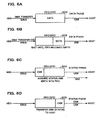
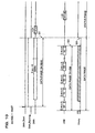
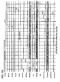
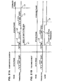
- the host When the host writes data to the device, it first performs a command phase (command transport) in which it transfers a CBW to the device, as shown in Fig. 5A. More specifically, the host transfers a token packet specifying the end point EP1 to the device, then transfers a CBW (see A1 in Fig. 2B and Fig. 3) to the end point EP1 of the device. This CBW comprises a write command. If the device returns a handshake (H.S) to the host, the command phase ends.
- command transport command transport
- the host transfers a token packet specifying the end point EP1 to the device, then transfers a CBW (see A1 in Fig. 2B and Fig. 3) to the end point EP1 of the device.
- This CBW comprises a write command.
- H.S handshake
- this comparative example has a problem in that the FIFO 602 is used in common for transferring both the data (IN data) and the CSW, so that the end of CSW write processing is delayed and thus the effective data transfer speed is deteriorated by that much.
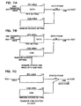
- this embodiment uses a method of switching between storage areas in the buffer in accordance with the switching of phase (transport).
- this embodiment makes it possible to return a data packet (CSW) at an early stage in answer to an IN token from the host, as shown in Fig. 7C. It is therefore possible to keep the loss of the bus zone to a minimum, enabling use of the high-speed data transfers of USB 2.0, and thus increasing the effective data transfer speed.
- CSW data packet
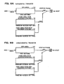
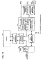
- a CSW0 area 18 (third storage area) into which a success status CSW0 (first status block packet) is written and a CSW1 area 19 (fourth storage area) into which a non-success status CSW1 (second status block packet) is written are provided as CSW areas (second storage areas) in the buffer, as shown in Fig. 8A.
- the information read area is switched when the phase has been switched.
- the EP1 register 43 also causes a flag SelCSW to be set to 0.
- This SelCSW flag is used for selecting which of the CSW0 area 61 and the CSW1 area 62 is to be connected to the bulk-in end point. For example, a bulk-in end point wherein EnCSW is set to 1 and SelCSW is also set to 1 is connected to the CSW0 area 61. A bulk-in end point wherein EnCSW is set to 1 and SelCSW is set to 0, on the other hand, is connected to the CSW1 area 62.
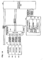
- the EP0, EP1, and EP2 address generation circuits 53, 54, and 55 each generate a write or read address AD2, AD3, or AD4 for SIEWrData or SIERdData, for the EP0, EP1, or EP2 area 63, 64, or 65 (start address a2, a3, or a4), respectively. More specifically, they generate sequentially incremented (or decremented) addresses AD2, AD3, and AD4 as start addresses a2, a3, and a4.
- a selector 57 comprised by the buffer management circuit 50 outputs SIEWrData from the transaction management circuit 36 to the buffer 60 as one of WrDataCSW, WrDataEP0, WrDataEP1, or WrDataEP2, based on EPsel from the end point management circuit 40.
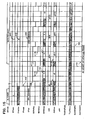
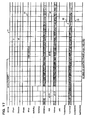
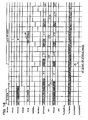
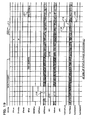
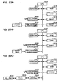
- Figs. 15, 16, and 17 show data transfer over the EBUS (second bus) when the status is successful.
- Fig. 15 is a timing waveform chart for the beginning of the status phase (the phase in which the success status is transferred) and Figs. 16 and 17 show the end of the status phase.
Landscapes
- Engineering & Computer Science (AREA)
- Theoretical Computer Science (AREA)
- Physics & Mathematics (AREA)
- General Engineering & Computer Science (AREA)
- General Physics & Mathematics (AREA)
- Information Transfer Systems (AREA)
- Communication Control (AREA)
Claims (11)
- Steuerungsgerät zur Datenübertragung für die Datenübertragung über einen Bus, aufweisend:dadurch gekennzeichnet, dasseinen Puffer mit einem ersten Speicherbereich (14) für eine erste Information und einem zweiten Speicherbereich (16) für eine zweite Information, wobei der erste und der zweite Speicherbereich (14, 16) für einen Endpunkt bereitgestellt werden, wenn eine Mehrzahl Informationstypen, die die erste und die zweite Information enthalten, als Informationen zugewiesen worden sind, die über diesen einen Endpunkt zu übertragen sind; undeine Puffer-Managementschaltung (50) zum Lesen von Informationen, die vom Endpunkt zu einem Host aus dem ersten Speicherbereich (14) für die erste Information während einer ersten Phase zu übertragen sind, in der die erste Information über den Bus übertragen wird, und zum Lesen von Informationen, die vom Endpunkt zu dem Host aus dem zweiten Speicherbereich (16) für die zweite Information während einer zweiten Phase zu übertragen sind, in der die zweite Information über den Bus übertragen wird;die erste Information ein Datenpaket ist; unddie zweite Information ein Statusblockpaket;
der zweite Speicherbereich (16) einen dritten Speicherbereich für ein erstes Statusblockpaket für den Erfolgsstatus und einen vierten Speicherbereich für ein zweites Statusblockpaket für den Nichterfolgs-Status aufweist; und
die Puffer-Managementschaltung (50) zum Lesen des ersten Statusblockpakets für den Erfolgsstatus aus dem dritten Speicherbereich, wenn der Status ein Erfolg ist, und zum Lesen des zweiten Statusblockpakets für den Nichterfolgs-Status aus dem vierten Speicherbereich, wenn der Status ein Nichterfolg ist, ausgeführt ist. - Gerät nach Anspruch 1, bei dem der erste Speicherbereich (14) ein Speicherbereich in der Weise ist, dass dort zuerst eingegebene Informationen von dort wieder zuerst ausgegeben werden; und
der zweite Speicherbereich (16) ein Speicherbereich mit Direktzugriff ist. - Gerät nach Anspruch 1 oder 2, so eingerichtet, dass ein Statusblockpaket im zweiten Speicherbereich (16) erstellt wird, während ein Datenpaket aus dem ersten Speicherbereich (14) gelesen wird.
- Gerät nach einem der Ansprüche 1 bis 3, so eingerichtet, dass ein Statusblockpaket, in das eine voreingestellte Information für den Erfolgsstatus gesetzt wird, vorab in den dritten Speicherbereich geschrieben wird.
- Gerät nach Anspruch 4, bei dem Tag-Informationen zum Verknüpfen eines Statusblockpakets und eines Befehlsblockpakets aus Informationen für das Statusblockpaket, in das eine voreingestellte Information gesetzt ist, aktualisiert werden, und das aktualisierte Statusblockpaket als das erste Statusblockpaket aus dem dritten Speicherbereich gelesen wird.
- Gerät nach einem der Ansprüche 1 bis 5, bei dem ein Lesebereich für Informationen, die von einem Endpunkt zu einem Host zu übertragen sind, vom ersten Speicherbereich (14) zum zweiten Speicherbereich (16) umgeschaltet wird, wenn bestimmt worden ist, dass eine Phase von der ersten Phase zur zweiten Phase umgeschaltet hat.
- Gerät nach Anspruch 6, so ausgeführt, dass bestimmt wird, dass eine Phase von der ersten Phase zur zweiten Phase umgeschaltet hat, wenn die Bedingung erfüllt ist, dass die Übertragungsverarbeitung zum Übertragen des Datenpakets über einen zweiten Bus und das Schreiben der Information in den ersten Speicherbereich (14) abgeschlossen sind und außerdem der erste Speicherbereich (14) leer geworden ist.
- Steuerungsgerät zur Datenübertragung gemäß einem der Ansprüche 1 bis 7, bei dem
der erste Speicherbereich (14) ein Statusspeicherbereich und der zweite Speicherbereich (16) ein Datenspeicherbereich ist;
die erste Phase eine Statusphase und die zweite Phase eine Datenphase ist; und
die Puffer-Managementschaltung (50) so ausgeführt ist, dass sie einen Informationslesebereich vom Datenspeicherbereich zum Statusspeicherbereich umschaltet und das Statusblockpaket, das vom Endpunkt zum Host zu übertragen ist, aus dem Statusspeicherbereich liest, wenn die Phase von der Datenphase zur Statusphase umschaltet. - Gerät nach einem der Ansprüche 1 bis 6, bei dem die Datenübertragung gemäß dem Universal Serial Bus (USB) Standard erfolgt.
- Elektronische Ausrüstung, aufweisend:das Gerät nach einem der Ansprüche 1 bis 9; undein Gerät zum Ausführen der Ausgabeverarbeitung, Abrufverarbeitung oder Speicherungsverarbeitung mit Daten, die über das Gerät und den Bus übertragen worden sind.
- Verfahren zur Datenübertragung über einen Bus, aufweisenddie erste Information als ein Datenpaket und die zweite Information als ein Statusblockpaketa) Bereitstellen eines ersten Speicherbereichs (14) für eine erste Information und eines zweiten Speicherbereichs (16) für eine zweite Information für einen Endpunkt in einem Puffer, wenn eine Mehrzahl Informationstypen, die die erste und die zweite Information enthalten, als Informationen zugewiesen worden sind, die über deren einen Endpunkt zu übertragen sind;b) Lesen von Informationen, die vom Endpunkt zu einem Host zu übertragen sind, aus dem ersten Speicherbereich (14) für die erste Information während einer ersten Phase, in der die erste Information über den Bus übertragen wird, und Lesen von Informationen, die vom Endpunkt zum Host zu übertragen sind, aus dem zweiten Speicherbereich (16) für die zweite Information während einer zweiten Phase, in der die zweite Information über den Bus übertragen wird; und
dadurch gekennzeichnet, dass
der zweite Speicherbereich (16) einen dritten Speicherbereich für ein erstes Statusblockpaket für den Erfolgsstatus und einen vierten Speicherbereich für ein zweites Statusblockpaket für den Nichterfolgs-Status aufweist, und
Schritt b) das Lesen des ersten Statusblockpakets für den Erfolgsstatus aus dem dritten Speicherbereich, wenn der Status ein Erfolg ist, und das Lesen des zweiten Statusblockpakets für den Nichterfolgs-Status aus dem vierten Speicherbereich, wenn der Status ein Nichterfolg ist, aufweist.
Applications Claiming Priority (2)
| Application Number | Priority Date | Filing Date | Title |
|---|---|---|---|
| JP2001143430 | 2001-05-14 | ||
| JP2001143430A JP3680763B2 (ja) | 2001-05-14 | 2001-05-14 | データ転送制御装置及び電子機器 |
Publications (3)
| Publication Number | Publication Date |
|---|---|
| EP1258798A2 EP1258798A2 (de) | 2002-11-20 |
| EP1258798A3 EP1258798A3 (de) | 2003-05-21 |
| EP1258798B1 true EP1258798B1 (de) | 2005-08-17 |
Family
ID=18989583
Family Applications (1)
| Application Number | Title | Priority Date | Filing Date |
|---|---|---|---|
| EP02010722A Expired - Lifetime EP1258798B1 (de) | 2001-05-14 | 2002-05-14 | Datentransfersteueranlage, elektronisches Gerät und Datentransfersteuerverfahren |
Country Status (8)
| Country | Link |
|---|---|
| US (2) | US7007112B2 (de) |
| EP (1) | EP1258798B1 (de) |
| JP (1) | JP3680763B2 (de) |
| KR (1) | KR100474221B1 (de) |
| CN (1) | CN1213372C (de) |
| AT (1) | ATE302444T1 (de) |
| DE (1) | DE60205531T2 (de) |
| TW (1) | TW571232B (de) |
Families Citing this family (18)
| Publication number | Priority date | Publication date | Assignee | Title |
|---|---|---|---|---|
| US7596709B2 (en) * | 2000-12-30 | 2009-09-29 | Intel Corporation | CPU power management based on utilization with lowest performance mode at the mid-utilization range |
| JP3680763B2 (ja) * | 2001-05-14 | 2005-08-10 | セイコーエプソン株式会社 | データ転送制御装置及び電子機器 |
| US7080189B1 (en) * | 2002-05-31 | 2006-07-18 | Cypress Semiconductor Corp. | USB device communication |
| JP2005293427A (ja) * | 2004-04-02 | 2005-10-20 | Matsushita Electric Ind Co Ltd | データ転送処理装置及びデータ転送処理方法 |
| JP4412191B2 (ja) * | 2005-02-04 | 2010-02-10 | セイコーエプソン株式会社 | データ転送制御装置及び電子機器 |
| JP4293141B2 (ja) * | 2005-02-18 | 2009-07-08 | セイコーエプソン株式会社 | データ転送制御装置及び電子機器 |
| JP2006235994A (ja) * | 2005-02-24 | 2006-09-07 | Nec Electronics Corp | ブリッジシステム、ブリッジシステム制御方法、情報処理機器、周辺機器及びプログラム |
| JP2007080244A (ja) * | 2005-08-19 | 2007-03-29 | Ricoh Co Ltd | データ転送装置及び画像形成装置 |
| JP2007214786A (ja) * | 2006-02-08 | 2007-08-23 | Toshiba Corp | 携帯型撮像装置 |
| JP2007249938A (ja) * | 2006-02-14 | 2007-09-27 | Matsushita Electric Ind Co Ltd | Usbホストシステム、avデータ再生装置およびavデータ記録装置 |
| JP4369486B2 (ja) | 2007-02-01 | 2009-11-18 | 富士通株式会社 | データ転送装置、半導体集積回路、および処理状況通知方法 |
| US20080263242A1 (en) * | 2007-04-18 | 2008-10-23 | Adrian Bica | Usb flash media extender |
| US8315269B1 (en) | 2007-04-18 | 2012-11-20 | Cypress Semiconductor Corporation | Device, method, and protocol for data transfer between host device and device having storage interface |
| TW200844841A (en) * | 2007-05-10 | 2008-11-16 | Realtek Semiconductor Corp | Method for expediting data access of universal serial bus stoarage device |
| TWI448902B (zh) | 2007-08-24 | 2014-08-11 | Cypress Semiconductor Corp | 具頁存取基礎處理器介面之橋接裝置 |
| US8090894B1 (en) | 2007-09-21 | 2012-01-03 | Cypress Semiconductor Corporation | Architectures for supporting communication and access between multiple host devices and one or more common functions |
| TW200945052A (en) * | 2008-04-21 | 2009-11-01 | Ralink Technology Corp | Method for increasing USB transmission rate |
| KR102208656B1 (ko) * | 2015-04-09 | 2021-01-28 | 한국전자통신연구원 | 시리얼 통신 제어 장치 및 방법 |
Family Cites Families (21)
| Publication number | Priority date | Publication date | Assignee | Title |
|---|---|---|---|---|
| IL100127A0 (en) * | 1991-03-11 | 1992-08-18 | Future Domain Corp | Scsi controller |
| JP2868141B2 (ja) * | 1992-03-16 | 1999-03-10 | 株式会社日立製作所 | ディスクアレイ装置 |
| US6185641B1 (en) * | 1997-05-01 | 2001-02-06 | Standard Microsystems Corp. | Dynamically allocating space in RAM shared between multiple USB endpoints and USB host |
| US5944797A (en) | 1997-05-28 | 1999-08-31 | International Business Machines Corporation | Data mover hardware controlled processing in a commanding system and in a commanded system for controlling frame communications on a link |
| EP0893755B1 (de) | 1997-07-21 | 2004-05-06 | Infineon Technologies AG | Pufferspeicheranordnung |
| US5974486A (en) * | 1997-08-12 | 1999-10-26 | Atmel Corporation | Universal serial bus device controller comprising a FIFO associated with a plurality of endpoints and a memory for storing an identifier of a current endpoint |
| US6157975A (en) | 1998-01-07 | 2000-12-05 | National Semiconductor Corporation | Apparatus and method for providing an interface to a compound Universal Serial Bus controller |
| US6145045A (en) | 1998-01-07 | 2000-11-07 | National Semiconductor Corporation | System for sending and receiving data on a Universal Serial Bus (USB) using a memory shared among a number of end points |
| US6065087A (en) * | 1998-05-21 | 2000-05-16 | Hewlett-Packard Company | Architecture for a high-performance network/bus multiplexer interconnecting a network and a bus that transport data using multiple protocols |
| US6389495B1 (en) * | 1999-01-16 | 2002-05-14 | Cypress Semiconductor Corp. | Dedicated circuit and method for enumerating and operating a peripheral device on a universal serial bus |
| AU5774200A (en) * | 1999-06-28 | 2001-01-31 | Sangate Systems Inc. | Intelligent splitter, system, and methods of use |
| JP3608441B2 (ja) | 1999-07-15 | 2005-01-12 | セイコーエプソン株式会社 | データ転送制御装置及び電子機器 |
| KR20010026922A (ko) * | 1999-09-09 | 2001-04-06 | 윤종용 | 유에스비 디바이스의 엔드포인트 컨트롤러 |
| JP4329188B2 (ja) * | 1999-11-05 | 2009-09-09 | 船井電機株式会社 | データ転送制御装置 |
| JP2001229115A (ja) * | 2000-02-17 | 2001-08-24 | Matsushita Electric Ind Co Ltd | Atapiコマンド処理方式 |
| US6779061B1 (en) * | 2000-05-09 | 2004-08-17 | Cypress Semiconductor Corp. | Method and apparatus implementing a FIFO with discrete blocks |
| JP3415567B2 (ja) * | 2000-06-21 | 2003-06-09 | エヌイーシーマイクロシステム株式会社 | Usb転送制御方法およびusbコントローラ |
| US6618788B1 (en) * | 2000-09-27 | 2003-09-09 | Cypress Semiconductor, Inc. | ATA device control via a packet-based interface |
| JP3680763B2 (ja) * | 2001-05-14 | 2005-08-10 | セイコーエプソン株式会社 | データ転送制御装置及び電子機器 |
| JP3680762B2 (ja) | 2001-05-14 | 2005-08-10 | セイコーエプソン株式会社 | データ転送制御装置及び電子機器 |
| JP3870717B2 (ja) | 2001-05-14 | 2007-01-24 | セイコーエプソン株式会社 | データ転送制御装置及び電子機器 |
-
2001
- 2001-05-14 JP JP2001143430A patent/JP3680763B2/ja not_active Expired - Lifetime
-
2002
- 2002-05-09 US US10/140,829 patent/US7007112B2/en not_active Expired - Lifetime
- 2002-05-10 KR KR10-2002-0025893A patent/KR100474221B1/ko not_active Expired - Fee Related
- 2002-05-13 TW TW091109910A patent/TW571232B/zh not_active IP Right Cessation
- 2002-05-14 AT AT02010722T patent/ATE302444T1/de not_active IP Right Cessation
- 2002-05-14 EP EP02010722A patent/EP1258798B1/de not_active Expired - Lifetime
- 2002-05-14 CN CNB021193827A patent/CN1213372C/zh not_active Expired - Fee Related
- 2002-05-14 DE DE60205531T patent/DE60205531T2/de not_active Expired - Lifetime
-
2005
- 2005-11-02 US US11/264,170 patent/US7237047B2/en not_active Expired - Lifetime
Also Published As
| Publication number | Publication date |
|---|---|
| JP3680763B2 (ja) | 2005-08-10 |
| EP1258798A3 (de) | 2003-05-21 |
| KR20020087860A (ko) | 2002-11-23 |
| CN1213372C (zh) | 2005-08-03 |
| US20060053329A1 (en) | 2006-03-09 |
| US20020169905A1 (en) | 2002-11-14 |
| DE60205531D1 (de) | 2005-09-22 |
| DE60205531T2 (de) | 2006-03-30 |
| JP2002344538A (ja) | 2002-11-29 |
| CN1385793A (zh) | 2002-12-18 |
| US7237047B2 (en) | 2007-06-26 |
| KR100474221B1 (ko) | 2005-03-08 |
| US7007112B2 (en) | 2006-02-28 |
| TW571232B (en) | 2004-01-11 |
| ATE302444T1 (de) | 2005-09-15 |
| EP1258798A2 (de) | 2002-11-20 |
Similar Documents
| Publication | Publication Date | Title |
|---|---|---|
| EP1260909B1 (de) | Datensteueranlage, elektronisches Gerät und Datenübertragungssteuerverfahren | |
| EP1260908B1 (de) | Datensteueranlage, elektronisches Gerät und Verfahren zur Übertragungssteuerung | |
| EP1258798B1 (de) | Datentransfersteueranlage, elektronisches Gerät und Datentransfersteuerverfahren | |
| US6839347B1 (en) | Data transfer controller and electronic device | |
| US7028109B2 (en) | Data transfer control device including buffer controller with plurality of pipe regions allocated to plurality of endpoints | |
| US20050010702A1 (en) | Data transfer control device, electronic instrument, and data transfer control method | |
| US20040073697A1 (en) | Data transfer control device, electronic equipment, and data transfer control method | |
| US6857028B1 (en) | Data transfer control device and electronic equipment | |
| US7409471B2 (en) | Data transfer control device for data transfer over a bus, electronic equipment and method for data transfer over a bus | |
| US7359996B2 (en) | Data transfer control device, electronic equipment, and data transfer control method | |
| US7469304B2 (en) | Data transfer control device, electronic equipment, and method for a data transfer through a bus, the data transfer control device including a register and a packet buffer that are commonly used during a host operation and a peripheral operation | |
| US7428600B2 (en) | Data transfer control device, electronic equipment, and data transfer control method | |
| KR100563418B1 (ko) | 통신 컨트롤러 및 통신 방법 | |
| JP2000112878A (ja) | デ―タ処理装置内の転送要求タイミングを制御するための装置および方法 | |
| JP2004295594A (ja) | データ転送制御装置、電子機器及びデータ転送制御方法 |
Legal Events
| Date | Code | Title | Description |
|---|---|---|---|
| PUAI | Public reference made under article 153(3) epc to a published international application that has entered the european phase |
Free format text: ORIGINAL CODE: 0009012 |
|
| AK | Designated contracting states |
Kind code of ref document: A2 Designated state(s): AT BE CH CY DE DK ES FI FR GB GR IE IT LI LU MC NL PT SE TR |
|
| AX | Request for extension of the european patent |
Free format text: AL;LT;LV;MK;RO;SI |
|
| PUAL | Search report despatched |
Free format text: ORIGINAL CODE: 0009013 |
|
| RIC1 | Information provided on ipc code assigned before grant |
Ipc: 7G 06F 13/42 B Ipc: 7G 06F 5/06 A Ipc: 7G 06F 13/38 B |
|
| AK | Designated contracting states |
Designated state(s): AT BE CH CY DE DK ES FI FR GB GR IE IT LI LU MC NL PT SE TR |
|
| AX | Request for extension of the european patent |
Extension state: AL LT LV MK RO SI |
|
| 17P | Request for examination filed |
Effective date: 20031030 |
|
| AKX | Designation fees paid |
Designated state(s): AT BE CH CY DE DK ES FI FR GB GR IE IT LI LU MC NL PT SE TR |
|
| 17Q | First examination report despatched |
Effective date: 20040121 |
|
| GRAP | Despatch of communication of intention to grant a patent |
Free format text: ORIGINAL CODE: EPIDOSNIGR1 |
|
| GRAS | Grant fee paid |
Free format text: ORIGINAL CODE: EPIDOSNIGR3 |
|
| GRAA | (expected) grant |
Free format text: ORIGINAL CODE: 0009210 |
|
| AK | Designated contracting states |
Kind code of ref document: B1 Designated state(s): AT BE CH CY DE DK ES FI FR GB GR IE IT LI LU MC NL PT SE TR |
|
| PG25 | Lapsed in a contracting state [announced via postgrant information from national office to epo] |
Ref country code: IT Free format text: LAPSE BECAUSE OF FAILURE TO SUBMIT A TRANSLATION OF THE DESCRIPTION OR TO PAY THE FEE WITHIN THE PRESCRIBED TIME-LIMIT;WARNING: LAPSES OF ITALIAN PATENTS WITH EFFECTIVE DATE BEFORE 2007 MAY HAVE OCCURRED AT ANY TIME BEFORE 2007. THE CORRECT EFFECTIVE DATE MAY BE DIFFERENT FROM THE ONE RECORDED. Effective date: 20050817 Ref country code: BE Free format text: LAPSE BECAUSE OF FAILURE TO SUBMIT A TRANSLATION OF THE DESCRIPTION OR TO PAY THE FEE WITHIN THE PRESCRIBED TIME-LIMIT Effective date: 20050817 Ref country code: FI Free format text: LAPSE BECAUSE OF FAILURE TO SUBMIT A TRANSLATION OF THE DESCRIPTION OR TO PAY THE FEE WITHIN THE PRESCRIBED TIME-LIMIT Effective date: 20050817 Ref country code: CH Free format text: LAPSE BECAUSE OF FAILURE TO SUBMIT A TRANSLATION OF THE DESCRIPTION OR TO PAY THE FEE WITHIN THE PRESCRIBED TIME-LIMIT Effective date: 20050817 Ref country code: TR Free format text: LAPSE BECAUSE OF FAILURE TO SUBMIT A TRANSLATION OF THE DESCRIPTION OR TO PAY THE FEE WITHIN THE PRESCRIBED TIME-LIMIT Effective date: 20050817 Ref country code: AT Free format text: LAPSE BECAUSE OF FAILURE TO SUBMIT A TRANSLATION OF THE DESCRIPTION OR TO PAY THE FEE WITHIN THE PRESCRIBED TIME-LIMIT Effective date: 20050817 Ref country code: LI Free format text: LAPSE BECAUSE OF FAILURE TO SUBMIT A TRANSLATION OF THE DESCRIPTION OR TO PAY THE FEE WITHIN THE PRESCRIBED TIME-LIMIT Effective date: 20050817 |
|
| REG | Reference to a national code |
Ref country code: GB Ref legal event code: FG4D |
|
| REG | Reference to a national code |
Ref country code: CH Ref legal event code: EP |
|
| REG | Reference to a national code |
Ref country code: IE Ref legal event code: FG4D |
|
| REF | Corresponds to: |
Ref document number: 60205531 Country of ref document: DE Date of ref document: 20050922 Kind code of ref document: P |
|
| PG25 | Lapsed in a contracting state [announced via postgrant information from national office to epo] |
Ref country code: GR Free format text: LAPSE BECAUSE OF FAILURE TO SUBMIT A TRANSLATION OF THE DESCRIPTION OR TO PAY THE FEE WITHIN THE PRESCRIBED TIME-LIMIT Effective date: 20051117 Ref country code: DK Free format text: LAPSE BECAUSE OF FAILURE TO SUBMIT A TRANSLATION OF THE DESCRIPTION OR TO PAY THE FEE WITHIN THE PRESCRIBED TIME-LIMIT Effective date: 20051117 Ref country code: SE Free format text: LAPSE BECAUSE OF FAILURE TO SUBMIT A TRANSLATION OF THE DESCRIPTION OR TO PAY THE FEE WITHIN THE PRESCRIBED TIME-LIMIT Effective date: 20051117 |
|
| PG25 | Lapsed in a contracting state [announced via postgrant information from national office to epo] |
Ref country code: ES Free format text: LAPSE BECAUSE OF FAILURE TO SUBMIT A TRANSLATION OF THE DESCRIPTION OR TO PAY THE FEE WITHIN THE PRESCRIBED TIME-LIMIT Effective date: 20051128 |
|
| PG25 | Lapsed in a contracting state [announced via postgrant information from national office to epo] |
Ref country code: PT Free format text: LAPSE BECAUSE OF FAILURE TO SUBMIT A TRANSLATION OF THE DESCRIPTION OR TO PAY THE FEE WITHIN THE PRESCRIBED TIME-LIMIT Effective date: 20060117 |
|
| REG | Reference to a national code |
Ref country code: CH Ref legal event code: PL |
|
| ET | Fr: translation filed | ||
| PG25 | Lapsed in a contracting state [announced via postgrant information from national office to epo] |
Ref country code: IE Free format text: LAPSE BECAUSE OF NON-PAYMENT OF DUE FEES Effective date: 20060515 |
|
| PG25 | Lapsed in a contracting state [announced via postgrant information from national office to epo] |
Ref country code: MC Free format text: LAPSE BECAUSE OF NON-PAYMENT OF DUE FEES Effective date: 20060531 |
|
| PLBE | No opposition filed within time limit |
Free format text: ORIGINAL CODE: 0009261 |
|
| STAA | Information on the status of an ep patent application or granted ep patent |
Free format text: STATUS: NO OPPOSITION FILED WITHIN TIME LIMIT |
|
| 26N | No opposition filed |
Effective date: 20060518 |
|
| REG | Reference to a national code |
Ref country code: IE Ref legal event code: MM4A |
|
| PG25 | Lapsed in a contracting state [announced via postgrant information from national office to epo] |
Ref country code: LU Free format text: LAPSE BECAUSE OF NON-PAYMENT OF DUE FEES Effective date: 20060514 |
|
| PG25 | Lapsed in a contracting state [announced via postgrant information from national office to epo] |
Ref country code: CY Free format text: LAPSE BECAUSE OF FAILURE TO SUBMIT A TRANSLATION OF THE DESCRIPTION OR TO PAY THE FEE WITHIN THE PRESCRIBED TIME-LIMIT Effective date: 20050817 |
|
| REG | Reference to a national code |
Ref country code: FR Ref legal event code: PLFP Year of fee payment: 15 |
|
| PGFP | Annual fee paid to national office [announced via postgrant information from national office to epo] |
Ref country code: NL Payment date: 20160411 Year of fee payment: 15 |
|
| PGFP | Annual fee paid to national office [announced via postgrant information from national office to epo] |
Ref country code: DE Payment date: 20160510 Year of fee payment: 15 Ref country code: GB Payment date: 20160511 Year of fee payment: 15 |
|
| PGFP | Annual fee paid to national office [announced via postgrant information from national office to epo] |
Ref country code: FR Payment date: 20160412 Year of fee payment: 15 |
|
| REG | Reference to a national code |
Ref country code: DE Ref legal event code: R119 Ref document number: 60205531 Country of ref document: DE |
|
| REG | Reference to a national code |
Ref country code: NL Ref legal event code: MM Effective date: 20170601 |
|
| GBPC | Gb: european patent ceased through non-payment of renewal fee |
Effective date: 20170514 |
|
| REG | Reference to a national code |
Ref country code: FR Ref legal event code: ST Effective date: 20180131 |
|
| PG25 | Lapsed in a contracting state [announced via postgrant information from national office to epo] |
Ref country code: NL Free format text: LAPSE BECAUSE OF NON-PAYMENT OF DUE FEES Effective date: 20170601 |
|
| PG25 | Lapsed in a contracting state [announced via postgrant information from national office to epo] |
Ref country code: DE Free format text: LAPSE BECAUSE OF NON-PAYMENT OF DUE FEES Effective date: 20171201 Ref country code: GB Free format text: LAPSE BECAUSE OF NON-PAYMENT OF DUE FEES Effective date: 20170514 |
|
| PG25 | Lapsed in a contracting state [announced via postgrant information from national office to epo] |
Ref country code: FR Free format text: LAPSE BECAUSE OF NON-PAYMENT OF DUE FEES Effective date: 20170531 |