EP1258797A2 - Informationsverarbeitungsgerät und Verfahren zur Rücksetzsteuerung - Google Patents
Informationsverarbeitungsgerät und Verfahren zur Rücksetzsteuerung Download PDFInfo
- Publication number
- EP1258797A2 EP1258797A2 EP02251658A EP02251658A EP1258797A2 EP 1258797 A2 EP1258797 A2 EP 1258797A2 EP 02251658 A EP02251658 A EP 02251658A EP 02251658 A EP02251658 A EP 02251658A EP 1258797 A2 EP1258797 A2 EP 1258797A2
- Authority
- EP
- European Patent Office
- Prior art keywords
- reset
- hard
- process part
- information
- mpu
- Prior art date
- Legal status (The legal status is an assumption and is not a legal conclusion. Google has not performed a legal analysis and makes no representation as to the accuracy of the status listed.)
- Withdrawn
Links
Images


Classifications
-
- G—PHYSICS
- G06—COMPUTING OR CALCULATING; COUNTING
- G06F—ELECTRIC DIGITAL DATA PROCESSING
- G06F1/00—Details not covered by groups G06F3/00 - G06F13/00 and G06F21/00
- G06F1/24—Resetting means
Definitions
- the present invention generally relates to information processing apparatuses and methods of reset control, and more particularly, to an information processing apparatus and a method of reset control by which it is possible to implement resetting accurately in a simple structure.
- a related art operation apparatus securing a bus cycle when resetting a micro processor unit (MPU) is implemented is described in Japanese Laid-Open Patent Applications No. 5-127780, No. 6-231279, and No. 60-211545.
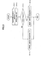
- FIG. 1 is a block diagram of a related art information processing apparatus.
- the related art information processing apparatus includes an MPU 11, a bus cycle detector 12, and a reset mask circuit 13. Resetting the MPU 11 is implemented, after transmitting an input of external resetting to the MPU 11 is delayed until a bus cycle of the MPU 11 is completed.
- a plurality of buses controlled by the MPU such as a peripheral component interconnect (PCI) bus, an accelerated graphic port (AGP), or a cache, may work independently because the MPU has performed high level functions.
- PCI peripheral component interconnect
- AGP accelerated graphic port
- a circuit for recognizing a bus cycle of an internal random access memory (RAM), an internal read only memory (ROM), the cache, an external memory, or the like may be very complicated with regard to an MPU built in a large scale integration circuit (LSI).
- Another and more specific object of the present invention is to provide an information processing apparatus and a method of reset control so that a reset process can be implemented by a program based on an interrupt signal and a hard reset process can be implemented by a hard reset signal. As a result, it is possible to implement resetting accurately in a simple structure.
- an information processing apparatus including a process part for implementing a reset process by a program based on an interrupt signal and hard-resetting by a hard reset signal, an information holding part for holding switching information that determines whether an external reset input is supplied to the process part as the interrupt signal or the hard reset signal, and a switch part for switching a supply of the external reset input to the process part as either the interrupt signal or the hard reset signal based on the switching information.
- the switching information may be held at the information holding part by the process part after the process part is booted.
- a method of reset control for a process part of an information processing apparatus including the steps of a) switching a supply of an external reset input to the process part as either an interrupt signal or a hard reset signal, based on switching information that is set beforehand, and b) implementing a reset process by a program based on the interrupt signal or hard-resetting by the hard reset signal.
- the switching information in step a) may be set by the process part after the process part is booted.
- the information processing apparatus may further include a back up part for implementing a back up process when system electric power is shut off, and wherein the information holding part may include a back up information holding part for holding information that indicates whether the back up part is in a back up state, and the switch part switches the supply of the external reset input to the process part as the hard reset signal, when the information that indicates whether the back up part is in the back up state is held at the back up information holding part.
- the information holding part may include a back up information holding part for holding information that indicates whether the back up part is in a back up state, and the switch part switches the supply of the external reset input to the process part as the hard reset signal, when the information that indicates whether the back up part is in the back up state is held at the back up information holding part.
- the external reset input in step a) may be supplied to the process part as the hard reset signal after system electric power is shut off and a back up process is implemented.
- the process part may output self-reset information after a program being implemented is terminated when the interrupt signal is supplied to the process part
- the information holding part may include a self-reset information holding part for holding self-reset information, and hard-resetting may be implemented for the process part when the self-reset information is active.
- a program being implemented may be terminated and hard-resetting may be implemented for the process part by the process part when the interrupt signal is supplied to the process part in step a).
- FIG. 2 is a block diagram of a first embodiment of the present invention.
- an information processing apparatus 100 of the first embodiment of the present invention includes an MPU 101, a storage 102, an interface circuit 103, a reset switch register 104, a switch circuit 105, a self-reset register 106, a logical product (AND) gate 107, and a reset switch circuit 108.
- the MPU 101 implements a data process based on a program including a reset switch control program stored in the storage 102.
- the storage 102 includes a ROM, a RAM, and a hard disk drive (HDD) and stores a program and data.
- the interface circuit 103 implements exchanging data between the MPU 101 and a peripheral not shown in FIG. 2.
- a flag is set at the reset switch register 104 by the MPU 101.
- the flag is used for distinguishing whether an external reset input is used as a hard reset input or a reset interrupt. For example, a flag "1" is set as a hard reset and a flag "0" is set as a reset interrupt.
- the external reset input is supplied from the reset switch circuit 108 to the switch circuit 105.
- the flag held at the reset switch register 104 is supplied to the switch circuit 105.
- the external reset input from the reset switch circuit 108 is supplied to the MPU 101 as a reset interrupt signal.
- a non-maskable interrupt (NMI) signal is used as the reset interrupt signal.
- NMI non-maskable interrupt
- a flag for deciding whether or not self-resetting is implemented based on an issued order of self-reset by the MPU 101 is set at the self-reset register 106.
- the flag held at the self-reset register 106 is supplied to the AND gate 107.
- the AND gate outputs an AND logic of the output of the switch circuit 105 and the flag held at the self-reset register 106.
- An output of the AND gate 107 is supplied to the MPU 101 as a hard reset signal.
- the reset switch circuit 108 includes a switch operated by a user.
- the reset switch circuit 108 outputs a binary signal corresponding to an operation by the user. Generally the output of the reset switch circuit 108 is "1". During a reset operation by the user, the output of the reset switch circuit 108 is "0".
- FIG. 3 is a flow chart of a reset switch processing program of a first embodiment according to the present invention.
- the MPU 101 refers to a user set stored in the storage 102 in step S1-2. In step S1-3, the MPU 101 determines whether the user set is a hard reset or a reset interrupt.
- the MPU 101 determines the user set is the hard reset in step S1-3, the MPU 101 sets the flag "1" at the reset switch register 104 in step S1-4. If the MPU 101 determines the user set is the reset interrupt in step S1-3, the MPU 101 sets the flag "0" in step S1-5.
- the switch circuit 105 is switched so that an output of the reset switch circuit 108 is supplied to the MPU 101 as the reset interrupt, as shown by a solid line in FIG. 2. If the flag "1" is set at the reset switch register 104, the switch circuit 105 is switched so that the output of the reset switch circuit 108 is supplied to the AND gate 107, as shown by a doted line in FIG. 2.
- FIG. 4 is a flow chart of the operation of the MPU when a reset operation is implemented according to the first embodiment of the present invention.
- FIG. 5-(A) is a timing chart of an input reset when a reset operation is implemented according to the first embodiment of the present invention.
- FIG. 5-(B) is a timing chart of a reset interrupt when a reset operation is implemented according to the first embodiment of the present invention.
- FIG. 5-(C) is a timing chart of an internal reset signal when a reset operation is implemented according to the first embodiment of the present invention.
- FIG. 6-(A) is an additional timing chart of an input reset when a reset operation is implemented according to the first embodiment of the present invention.
- FIG. 6-(B) is an additional timing chart of a reset interrupt when a reset operation is implemented according to the first embodiment of the present invention.
- FIG. 6-(C) is an additional timing chart of a internal reset signal when a reset operation is implemented according to the first embodiment of the present invention.
- the switch circuit 105 When the flag "1" is set at the reset switch register 104, that is, the hard reset is selected, the switch circuit 105 is connected to the AND gate 107 as shown by the dotted line in FIG. 2. Hence, the external reset input is supplied from the reset switch circuit 108 to the AND gate 107 directly.
- FIG. 5-(A) when the flag of the external reset input is "0", namely active, the output of the AND gate 107 is "0" regardless of the flag of the self-reset register 106. Since a hard reset terminal of the MPU 101 is low-active, the internal reset signal of the MPU 101 is "0", namely active, as shown in FIG. 5-(C). As a result, resetting of the MPU 101 is implemented. That is, resetting of the internal register is implemented directly by the external reset.
- step S2-2 a program being implemented is terminated in step S2-2.
- step S2-2 After the program being implemented is terminated in step S2-2, the flag "0" is set at the self-reset register 106 in step S2-3 and the output of the AND gate 107 is "0". That is, a hard reset terminal of the MPU 101 is "0". Accordingly, the internal reset signal of the MPU 101 is "0", namely active, as shown in FIG. 6-(C) and thereby resetting of the MPU 101 is implemented.
- the user can set the resetting operation of the MPU 101 by the external reset input, as a reset by a reset interrupt or a hard reset. That is, the self-resetting is issued by software.
- the hard-resetting may be implemented after an electric power back up is implemented, as mentioned by the following second embodiment.
- FIG. 7 is a block diagram of a second embodiment of the present invention.
- parts that are the same as the parts shown in FIG. 2 are given the same reference numerals, and explanation thereof will be omitted.
- the hard-resetting can be implemented whenever system electric power is shut off.
- an information processing apparatus 200 is normally operated by system electric power 201.
- system electric power 201 When the system electric power 201 is shut off, only a minimum essential circuit is operated by a back up part 202.
- the information processing apparatus 200 includes a back up primary factor register 203 instead of the reset switch register 104 and the self-reset register 106 of the information processing apparatus 100.
- the switch control circuit 105 is controlled by the back up primary factor register 203.
- the back up part 202 includes a back up electric supply 211, a back up control circuit 212, a back up memory 213, and a real time clock (RTC) 214.
- RTC real time clock
- the back up primary factor register 203 is, for example, comprised of a flip-flop circuit. A flag "0" is written in the back up primary factor register 203 based on an order of the MPU 101.
- the back up control signal is supplied from the back up control circuit 212 to a set terminal of the back up primary factor register 203. When the back up control signal is "0", the back up control signal becomes active. That means the information processing apparatus 200 is in a back up state. When the back up control signal is "0", "1" is set at the back up primary factor register 203.
- FIG. 8 is a flow chart of an operation of the MPU of the second embodiment.
- step S3-1 the MPU 101 reads the back up primary factor register 203.
- step S3-2 the MPU 101 determines whether or not the back up primary factor is set inside of the MPU 101.
- the MPU 101 sets "0" at the back up primary factor register 203 in step S3-3 and an output of the back up primary factor register 203 is "0".
- the switch circuit 105 is connected to the MPU 101 as shown by a solid line in FIG. 7.
- an external reset input from the reset switch circuit 108 is supplied to the MPU 101 as a reset interrupt signal.
- the MPU 101 After the MPU 101 is booted completely, when an external reset input from the reset switch circuit 108 is "0", namely active, the reset interrupt signal is also "0", namely active. Therefore, the MPU 101 implements a resetting process based on a normal reset interrupt, which is a resetting process occurring after an implementing process is completed.
- an operation state of the MPU 101 is determined through an operation state of the back up part 202 in this embodiment.
- the external reset input is supplied to the MPU 101 as a hard reset signal.
- the external reset input is supplied to the MPU 101 as a rest interrupt signal.
- FIG. 9 is a block diagram of a third embodiment of the present invention.
- parts that are the same as the parts shown in FIG. 2 are given the same reference numerals, and explanation thereof will be omitted.
- an information processing apparatus 300 has a structure in which resetting is implemented accurately. It is controlled, whether the external reset input is supplied from the reset switch circuit 108 to the MPU 101 as a reset interrupt signal or a hard reset signal, by the self-reset register 106, the back up primary factor register 203, a reset primary factor register 301, the switch circuit 105, the AND gate 107, and an OR gate 302.
- the reset primary factor register 301 When the output of the self-reset register 106 is "0", namely active, the reset primary factor register 301 is "1" namely active. Based on an order from the MPU 101, the reset primary factor register 301 is "0", namely clear.
- An output of the back up primary factor register 203 and an output of the reset primary factor register 301 are supplied to the OR gate 302.
- the OR gate 302 outputs an OR logic between the output of the back up primary factor register 203 and the output of the reset primary factor register 301.
- the output of the OR gate 302 is supplied to the switch circuit 105.
- the switch circuit 105 supplies the external reset input from the reset switch circuit 108 to the MPU 101 as a reset interrupt signal when the output of the OR gate 302 is "0".
- the switch circuit 105 supplies the external reset input from the reset switch circuit 108 to the MPU 101 as a hard reset signal when the output of the OR gate 302 is "1".
- the self-reset register 106 When the MPU 101 is booted, the self-reset register 106 is "1" and the reset primary factor register 301 is "0". As described in the second embodiment of the present invention, since the back up primary factor register 203 is "0", namely active, the external reset input is supplied from the switch circuit 105 to the AND gate 107 as shown by a doted line in FIG. 9. The AND gate 107 outputs an AND logic between an input from the switch circuit 105 and the self-reset register 106. Hence, when the external reset input to the MPU 101 is "0", namely active, the hard reset signal has the flag "0", namely becomes active. Accordingly, hard-resetting to the MPU 101 is implemented. After the MPU 101 is booted, the "1" is set at the back up primary factor register 203 by a program which the MPU implements.
- FIG. 10 is a flow chart of an operation of the MPU 101 according to the third embodiment of the present invention.
- step S4-1 When the external reset input from the reset switch circuit 108 is "0", namely active, in step S4-1, the reset interrupt signal is "0". Hence resetting to the MPU 101 is implemented by reset interrupt. When resetting of the MPU 101 is implemented by the reset interrupt, the MPU 101 completes an implementing process in step S4-2.
- the MPU 101 sets "0" at the self-reset register 106 in step S4-3, so that "1" is set at the reset primary factor register 301 and an output of the OR gate 302 is "1".
- the switch circuit 105 is switched as shown by a doted line in FIG. 9. Therefore, in this case, when the external reset input from the reset switch circuit 108 is "0", namely active, the MPU 101 is implemented hard-resetting so that the MPU 101 is reset accurately.
- a hard reset signal which is an output of the AND gate 107, is "0", namely active, so that hard-resetting to the MPU 101 is implemented.
- the switch circuit 105 supplies the external reset input from the reset switch circuit 108 to the MPU 101 as a reset interrupt signal, as shown by a solid line in FIG. 9
- the external reset input can be supplied from the reset switch circuit 108 to the MPU 101 as a hard reset signal.
- the external reset input can be supplied to the MPU 101 as a reset interrupt signal.
- the switch circuit 105 can be switched by the reset primary factor register 301, as the external reset input is supplied as a hard reset signal.
- the reset operation can be implemented by one external reset input, no contradiction regarding a reset operation may occur inside of the MPU 101. Hence, the MPU 101 can implement a reset process accurately.
- the MPU can implement a process by clearing contents of the respective registers. Therefore, the operation of the MPU 101 can be simplified.
- the present invention is not limited to these embodiments, but variations and modifications may be made without departing from the scope of the present invention.
- the logic is set so that a signal for resetting is low active in the above mentioned embodiments, the signal may be low active or some of the signals may be low active or high active.
- the reset switch circuit in the above mentioned embodiments may be comprised by a different chip from the MPU 101 or mounted on an LSI of one chip.
Landscapes
- Engineering & Computer Science (AREA)
- Theoretical Computer Science (AREA)
- Physics & Mathematics (AREA)
- General Engineering & Computer Science (AREA)
- General Physics & Mathematics (AREA)
- Microcomputers (AREA)
- Power Sources (AREA)
Applications Claiming Priority (2)
| Application Number | Priority Date | Filing Date | Title |
|---|---|---|---|
| JP2001145175 | 2001-05-15 | ||
| JP2001145175A JP2002341973A (ja) | 2001-05-15 | 2001-05-15 | 情報処理装置及びリセット制御方法 |
Publications (1)
| Publication Number | Publication Date |
|---|---|
| EP1258797A2 true EP1258797A2 (de) | 2002-11-20 |
Family
ID=18991030
Family Applications (1)
| Application Number | Title | Priority Date | Filing Date |
|---|---|---|---|
| EP02251658A Withdrawn EP1258797A2 (de) | 2001-05-15 | 2002-03-08 | Informationsverarbeitungsgerät und Verfahren zur Rücksetzsteuerung |
Country Status (3)
| Country | Link |
|---|---|
| US (1) | US20020174383A1 (de) |
| EP (1) | EP1258797A2 (de) |
| JP (1) | JP2002341973A (de) |
Families Citing this family (2)
| Publication number | Priority date | Publication date | Assignee | Title |
|---|---|---|---|---|
| US7089413B2 (en) * | 2003-03-05 | 2006-08-08 | Hewlett-Packard Development Company, L.P. | Dynamic computer system reset architecture |
| US8972763B2 (en) * | 2011-12-05 | 2015-03-03 | Intel Corporation | Method, apparatus, and system for energy efficiency and energy conservation including determining an optimal power state of the apparatus based on residency time of non-core domains in a power saving state |
Family Cites Families (4)
| Publication number | Priority date | Publication date | Assignee | Title |
|---|---|---|---|---|
| DE3421584A1 (de) * | 1984-06-09 | 1985-12-12 | Robert Bosch Gmbh, 7000 Stuttgart | Ruecksetzschaltung fuer mikroprozessoren |
| GB2305036B (en) * | 1994-09-10 | 1997-08-13 | Holtek Microelectronics Inc | Reset signal generator |
| US6144887A (en) * | 1996-12-09 | 2000-11-07 | Denso Corporation | Electronic control unit with reset blocking during loading |
| US6467007B1 (en) * | 1999-05-19 | 2002-10-15 | International Business Machines Corporation | Processor reset generated via memory access interrupt |
-
2001
- 2001-05-15 JP JP2001145175A patent/JP2002341973A/ja active Pending
-
2002
- 2002-03-08 EP EP02251658A patent/EP1258797A2/de not_active Withdrawn
- 2002-03-11 US US10/093,488 patent/US20020174383A1/en not_active Abandoned
Also Published As
| Publication number | Publication date |
|---|---|
| JP2002341973A (ja) | 2002-11-29 |
| US20020174383A1 (en) | 2002-11-21 |
Similar Documents
| Publication | Publication Date | Title |
|---|---|---|
| JP3105223B2 (ja) | マイクロコンピュータ,マイクロプロセッサおよびコア・プロセッサ集積回路用デバッグ周辺装置 | |
| US6675305B1 (en) | Power saving in a USB peripheral by providing gated clock signal to CSR block in response to a local interrupt generated when an operation is to be performed | |
| EP2580657B1 (de) | Informationsverarbeitungsvorrichtung und -verfahren | |
| JPH09167105A (ja) | オンチップデバッグシステム | |
| JPH06314213A (ja) | デバッグ装置 | |
| EP0702297A1 (de) | Datenprozessor mit Haltepunktschaltung und Methode dafür | |
| JP4319712B2 (ja) | 集積回路においてアクセス保護を備える方法および装置 | |
| JPH08194563A (ja) | コンピュータシステム | |
| US6691268B1 (en) | Method and apparatus for swapping state data with scan cells | |
| US7100033B2 (en) | Controlling the timing of test modes in a multiple processor system | |
| US20170329723A1 (en) | Protection Scheme for Embedded Code | |
| US6092219A (en) | Method for use of bus parking states to communicate diagnostic information | |
| JPH05324348A (ja) | シングルチップマイクロコンピュータ | |
| US20090177807A1 (en) | Reset method for application specific integrated circuits (asic) | |
| WO2005010747A2 (en) | Microcontroller with an interrupt structure having programmable priority levels with each priority level associated with a different register set | |
| EP1258797A2 (de) | Informationsverarbeitungsgerät und Verfahren zur Rücksetzsteuerung | |
| EP0721163A1 (de) | Informationsverarbeitungsvorrichtung zur Einstellung des Betriebsmodus | |
| CN120320932A (zh) | 基于龙芯软核的simon加解密硬件加速系统及方法 | |
| US5671424A (en) | Immediate system management interrupt source with associated reason register | |
| US20230090567A1 (en) | Device and method for two-stage transitioning between reduced power states | |
| JP2004070961A (ja) | 複数のイベントタイプをサポートする方法及びシステム | |
| JP4176920B2 (ja) | データ処理装置 | |
| US6016551A (en) | Method and apparatus for masking and unmasking a clock signal in an integrated circuit | |
| EP0501621A2 (de) | Adressenprädiktion und Kontrolle für das Lesen von Daten in Burstzyklus | |
| JP4551212B2 (ja) | 情報処理装置及びリセット制御方法 |
Legal Events
| Date | Code | Title | Description |
|---|---|---|---|
| PUAI | Public reference made under article 153(3) epc to a published international application that has entered the european phase |
Free format text: ORIGINAL CODE: 0009012 |
|
| AK | Designated contracting states |
Kind code of ref document: A2 Designated state(s): AT BE CH CY DE DK ES FI FR GB GR IE IT LI LU MC NL PT SE TR |
|
| AX | Request for extension of the european patent |
Free format text: AL;LT;LV;MK;RO;SI |
|
| STAA | Information on the status of an ep patent application or granted ep patent |
Free format text: STATUS: THE APPLICATION IS DEEMED TO BE WITHDRAWN |
|
| 18D | Application deemed to be withdrawn |
Effective date: 20071002 |