EP1256987B1 - Semiconductor LED flip-chip with high reflectivity dielectric coating on the mesa - Google Patents
Semiconductor LED flip-chip with high reflectivity dielectric coating on the mesa Download PDFInfo
- Publication number
- EP1256987B1 EP1256987B1 EP02076622.6A EP02076622A EP1256987B1 EP 1256987 B1 EP1256987 B1 EP 1256987B1 EP 02076622 A EP02076622 A EP 02076622A EP 1256987 B1 EP1256987 B1 EP 1256987B1
- Authority
- EP
- European Patent Office
- Prior art keywords
- layer
- contact
- light emitting
- emitting device
- dielectric
- Prior art date
- Legal status (The legal status is an assumption and is not a legal conclusion. Google has not performed a legal analysis and makes no representation as to the accuracy of the status listed.)
- Expired - Lifetime
Links
Images



Classifications
-
- H—ELECTRICITY
- H10—SEMICONDUCTOR DEVICES; ELECTRIC SOLID-STATE DEVICES NOT OTHERWISE PROVIDED FOR
- H10H—INORGANIC LIGHT-EMITTING SEMICONDUCTOR DEVICES HAVING POTENTIAL BARRIERS
- H10H20/00—Individual inorganic light-emitting semiconductor devices having potential barriers, e.g. light-emitting diodes [LED]
- H10H20/80—Constructional details
- H10H20/84—Coatings, e.g. passivation layers or antireflective coatings
- H10H20/841—Reflective coatings, e.g. dielectric Bragg reflectors
-
- H—ELECTRICITY
- H10—SEMICONDUCTOR DEVICES; ELECTRIC SOLID-STATE DEVICES NOT OTHERWISE PROVIDED FOR
- H10H—INORGANIC LIGHT-EMITTING SEMICONDUCTOR DEVICES HAVING POTENTIAL BARRIERS
- H10H20/00—Individual inorganic light-emitting semiconductor devices having potential barriers, e.g. light-emitting diodes [LED]
- H10H20/80—Constructional details
- H10H20/81—Bodies
- H10H20/819—Bodies characterised by their shape, e.g. curved or truncated substrates
-
- H—ELECTRICITY
- H10—SEMICONDUCTOR DEVICES; ELECTRIC SOLID-STATE DEVICES NOT OTHERWISE PROVIDED FOR
- H10H—INORGANIC LIGHT-EMITTING SEMICONDUCTOR DEVICES HAVING POTENTIAL BARRIERS
- H10H20/00—Individual inorganic light-emitting semiconductor devices having potential barriers, e.g. light-emitting diodes [LED]
- H10H20/80—Constructional details
- H10H20/81—Bodies
- H10H20/822—Materials of the light-emitting regions
- H10H20/824—Materials of the light-emitting regions comprising only Group III-V materials, e.g. GaP
- H10H20/825—Materials of the light-emitting regions comprising only Group III-V materials, e.g. GaP containing nitrogen, e.g. GaN
-
- H—ELECTRICITY
- H10—SEMICONDUCTOR DEVICES; ELECTRIC SOLID-STATE DEVICES NOT OTHERWISE PROVIDED FOR
- H10H—INORGANIC LIGHT-EMITTING SEMICONDUCTOR DEVICES HAVING POTENTIAL BARRIERS
- H10H20/00—Individual inorganic light-emitting semiconductor devices having potential barriers, e.g. light-emitting diodes [LED]
- H10H20/80—Constructional details
- H10H20/83—Electrodes
- H10H20/832—Electrodes characterised by their material
- H10H20/835—Reflective materials
-
- H—ELECTRICITY
- H10—SEMICONDUCTOR DEVICES; ELECTRIC SOLID-STATE DEVICES NOT OTHERWISE PROVIDED FOR
- H10W—GENERIC PACKAGES, INTERCONNECTIONS, CONNECTORS OR OTHER CONSTRUCTIONAL DETAILS OF DEVICES COVERED BY CLASS H10
- H10W72/00—Interconnections or connectors in packages
- H10W72/20—Bump connectors, e.g. solder bumps or copper pillars; Dummy bumps; Thermal bumps
Definitions
- LEDs Semiconductor light-emitting diodes
- Materials systems currently of interest in the manufacture of high-brightness LEDs capable of operation across the visible spectrum include Group III-V semiconductors, particularly binary, ternary, and quaternary alloys of gallium, aluminum, indium, and nitrogen, also referred to as III-nitride materials.
- III-nitride devices are epitaxially grown on sapphire, silicon carbide, or III-nitride substrates by metal-organic chemical vapor deposition (MOCVD), molecular beam epitaxy (MBE), or other epitaxial techniques. Some of these substrates are insulating or poorly conducting.
- MOCVD metal-organic chemical vapor deposition
- MBE molecular beam epitaxy
- Devices fabricated from semiconductor crystals grown on such substrates must have both the positive and the negative polarity electrical contacts to the epitaxially-grown semiconductor on the same side of the device.
- semiconductor devices grown on conducting substrates can be fabricated such that one electrical contact is formed on the epitaxially grown material and the other electrical contact is formed on the substrate.
- devices fabricated on conducting substrates may also be designed to have both contacts on the same side of the device on which the epitaxial material is grown in a flip-chip geometry so as to improve light extraction from LED chip, to improve the current-carrying capacity of the chip, or to improve the heat-sinking of the LED die.
- Fig. 1 illustrates a typical III-nitride LED device.
- Semiconductor layers including, for example, n-layer 12, active region 13, and p-layer 14 are epitaxially grown on substrate 11.
- P-contact 15 and n-contact 17 are formed on the same side of the device as described above.
- Electrical isolation between the p-contact 15 and the n-contact 17 is achieved by etching a mesa structure 18 into the device extending from the topmost layer down into the underlying n-layer and forming separate, defined p-contact 15 and n-contact 17.
- the LED is mounted to a submount assembly 22, which typically includes a submount on which the LED is mounted with solder bumps. The solder bumps create a gap between the submount and the LED.
- the connected LED and submount assembly are then typically encapsulated in a high index of refraction gel or epoxy.
- the high index gel or epoxy is selected to match the index of refraction of the sapphire substrate as closely as possible, since the light produced in the device is extracted through the sapphire substrate.
- the difference in index of refraction determines how much light is reflected at that interface, and how much light is transmitted through it. The larger the difference in index of refraction, the more light is reflected.
- the small difference between the index of refraction of the sapphire substrate and the high index gel encapsulating the device ensures that most of the light generated in the device that reaches the emitting surfaces of the sapphire substrate is extracted from the device.
- Photons are generated efficiently within active region 13, but extracting the photons from the semiconductor into the LED package and to the outside world is difficult, in part due to the high indices of refraction of the semiconductor layers. See, for example, Windisch et al., Applied Physics Letters, vol. 74, no. 16, p2256 (1999 ). Photons generated within the epitaxial semiconductor are incident upon either the interface between the semiconductor and substrate 11, the interface at mesa wall 18 between the semiconductor and the high index gel in submount assembly 22, or the interface between the semiconductor and the metal contacts. Photons incident on any of the three interfaces face a step in material refractive index.
- Such a step in refractive index causes a ray 20 incident on such an interface to be split into a transmitted portion 20a and a reflected portion 20b.
- Light transmitted out from mesa wall 18 i.e. portion 20a
- light lost through transmission at mesa wall 18 contributes to the low light extraction efficiency of semiconductor LEDs.
- the high index gel encapsulating the device results in a small difference in refractive index at the interface at mesa wall 18 between the semiconductor area between the contacts and the submount assembly. As a result, much of the light incident on this area is transmitted in the direction of the submount assembly, which causes significant optical loss. As described above, light extracted in this area towards the submount assembly cannot be usefully extracted from the package; rather, it is incident on the submount where it is absorbed.
- the device area between the contacts on a device such as that shown in Fig. 1 is estimated at 10% of the total area. This area includes the mesa wall and a small portion of semiconductor material parallel to the substrate and between the edge of each contact and the mesa wall.
- Methods of reducing such losses include the use of wafer fabrication techniques such as self-aligned metalization and tightened manufacturing tolerances to reduce the area between the contacts parallel to the substrate. Such wafer fabrication techniques may result in other problems such as increased reliability problems and difficulty in manufacturing. In addition, wafer fabrication techniques do not significantly reduce losses, since 3-D optical ray trace modeling of high index gel-encapsulated, III-nitride LED structures grown on sapphire shows that, of the light undesirably extracted from the LED chip in this direction, the majority is lost through the mesa wall rather than from any surface of the epitaxial material which runs parallel to the substrate surface on which the epitaxial semiconductor was grown. The light extracted at the mesa wall is on the order of 15% of the light generated within the LED, the exact figure depending on, among other factors, the mesa wall height and angle.
- Attenuation can occur at all places within the semiconductor, but is likely to be largest at the interfaces, for example between the semiconductor and the substrate; between the semiconductor and the contacts; in the active region; and in any nucleation layer present between the first semiconductor layer and the substrate.
- the further light propagates the more it is attenuated.
- Light rays travelling through the semiconductor with a large angle ⁇ the angle of propagation relative to the substrate, will require a longer path length to travel a given distance in the semiconductor resolved parallel to the substrate, compared with light rays with a small angle ⁇ . Each time a ray is reflected, the sign of the angle of propagation is reversed.
- a ray propagating at angle ⁇ will propagate at an angle - ⁇ upon reflection.
- Large angle ⁇ rays will pass a greater number of times through the active region and will be reflected off the various interfaces (and especially at the semiconductor/p-contact interface and at the semiconductor/substrate) a greater number of times.
- Such rays will therefore be subject to greater attenuation per unit distance of propagation in the x-direction than rays travelling at shallower angles ⁇ .
- most of the flux (optical power) incident on the mesa wall is incident on the mesa wall at shallow angles ⁇ .
- Fig. 2 illustrates a model of flux distribution on the mesa wall as a function of propagation angle ⁇ .
- a device with some absorption in the contacts e.g. a device with an aluminum p-contact
- 70% or more of the total flux incident on the mesa is incident at an angle -10 degrees ⁇ ⁇ 30 degrees.
- the proportion of flux incident on the mesa wall within this same angular range falls to about 60%.
- Japanese Patent Application JP 2000-31540A discloses a light emitting diode comprising an aluminum p-contact and reflective stack on the mesa walls comprising SiO 2 and TiO 2 .
- a highly reflective dielectric stack is formed on the mesa wall of a flip-chip LED.
- the layers of the dielectric stack are selected to maximize reflection of light incident at angles ranging from 10 degrees towards the substrate to 30 degrees away from the substrate.
- the dielectric stack is comprised of alternating low refractive index and high refractive index layers.
- the LED is a III-nitride device with a p-contact containing silver
- the dielectric stack layer adjacent to the mesa wall has a low refractive index compared to GaN
- the low refractive index layers are Al 2 O 3 .
- the mesa wall of a flip chip LED is coated with a highly-reflective (HR) dielectric stack of alternating layers of two or more dielectric materials of differing refractive indices.
- the HR stack reduces the light lost through the mesa wall by reflecting and thereby redirecting a larger portion of the guided light within the LED chip which is incident on the coated mesa wall such that the light may be usefully extracted from the LED through the substrate.
- the use of an HR stack on the mesa wall improves extraction efficiency from LED flip-chips with minimal added complexity to the chip design and fabrication.
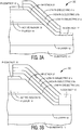
- Fig. 3A illustrates one embodiment of the present invention.
- An HR stack 21 is formed over the mesa wall separating p-contact 15 from n-contact 17.
- the mesa wall is typically formed at an angle of about 35 to 55 degrees to the plane of the substrate.
- HR stack 21 includes several discrete dielectric layers. HR stack 21 alternates between dielectric layers of low refractive index (layers 21a and 21c) compared to the semiconductor layers 12, 13, and 14 and dielectric layers of high refractive index (layer 21b) compared to the low refractive index layers.
- High refractive index layers generally have an index of refraction greater than 2.1, typically ranging from 2.1 to 2.7.
- Low refractive index generally have an index of refraction less than 1.8, typically between about 1.35 and 1.8.
- Materials having an index of refraction between 1.8 and 2.1 can be used as either high refractive index layers or low refractive index layers, depending on the composition of the other materials used in the HR stack.
- the layers are selected to create a difference in refractive index designed to maximize reflection of light incident on the HR stack.
- semiconductor layers 12, 13, and 14 are III-nitride materials, which have a high refractive index.
- dielectric layer 21a, the HR stack layer adjacent to semiconductor layers 12, 13, and 14 has a low refractive index.
- the HR stack is highly reflective of light incident on the mesa wall.
- HR stack layers 21 are selected and arranged to provide maximum reflectivity for light rays incident on the mesa wall at angles to the substrate surface ranging from -10 to 30 degrees.
- Low refractive index (RI) layers 21a, 21c are, for example, oxides, nitrides, and oxy-nitrides of silicon; aluminum oxides; fluorides of lithium, calcium and magnesium; and other materials containing these materials alloyed or doped with other materials.
- High RI layers 21b are, for example, oxides of titanium, zirconium, tantalum, and manganese; zinc sulfide; III-nitride materials having an index of refraction higher than about 2.1; and other materials based on these dielectrics and doped with other materials.
- Layers which could be considered as being either high or low refractive index layers are, for example, oxides of hafnium, tin, or antimony; III-nitride materials having a refractive index lower than about 2.1; and other materials containing these materials alloyed or doped with other materials.
- Table 1 illustrates the refractive indices of exemplary semiconductor layers, low refractive index layers, and high refractive index layers.
- the individual layers of HR stack 21 have a thickness of n ⁇ 4 1 2 where ⁇ is the wavelength of the propagating light in the particular layer, and n is any odd integer.
- ⁇ is the wavelength of the propagating light in the particular layer
- n is any odd integer.
- Light of a given frequency will have a different wavelength in the various semiconductor layers, in air, and in the various dielectric layers, all of which have a different refractive index.
- the individual layers of HR stack 21 have a thickness of n ⁇ sin ⁇ 4 where ⁇ is the angle between the mesa wall and the substrate.
- rays 31b, 32b, 33b all have to interfere constructively at material interface 21a->14, If they interfere destructively the stack becomes anti-reflecting rather than HR.
- the layer thicknesses described above allow constructive interference to occur.
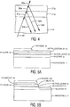
- Fig. 4 illustrates a simplified path of a light ray 35 through two layers of HR stack 21.
- Ray 35 passes through semiconductor layer 14 and is incident on dielectric layer 21a.
- the step in refractive index between semiconductor layer 14 and dielectric layer 21a causes a portion 31a of ray 35 to be transmitted through dielectric layer 21a and a portion 31b to be reflected.
- the transmitted portion 31a travels through dielectric layer 21a and is incident on dielectric layer 21b.
- the step in refractive index between dielectric layer 21a and dielectric layer 21b causes a portion 32a of ray 31a to be transmitted and a portion 32b to be reflected.
- transmitted portion 32a is incident on the next interface, once again a portion 33a is transmitted and a portion 33b is reflected.
- HR stack 21 reflects part of ray 35 (i.e. rays 31b, 32b, and 33b) back into semiconductor layer 14, where the light may be usefully extracted. Only a small part of ray 35, (i.e. ray 33a) is lost in a direction where it cannot be usefully extracted.
- LED 30 is a flip-chip device, formed on a SiC, sapphire, or III-nitride_substrate.
- P-contact 15 may be silver, a highly-reflecting silver alloy, or a multilayer stack of metals including silver.
- the low RI layers, including the HR stack layer in contact with the epitaxial layers, are typically aluminum oxide which enhances device reliability by suppressing migration of the silver into or across other layers of the device during device operation, thereby reducing the risk of short circuiting between the p- and n-contacts or across the p-n junction.
- Low RI layers which include oxides of silicon are avoided, because the presence of such oxides can enhance silver migration during device operation.
- the top layer of HR stack 21 is a reflective metal, though HR stack 21 does not require a metal as the top layer in order to be reflective.
- the top reflective metal layer may form part of the p- or n-contact and may be overlapped with the other contact to increase the current carrying capacity of the selected contact.
- the n-contact 17 overlays the HR stack.
- a portion of the n-contact, on the left hand side of Fig. 3B overlays a portion of p-contact 15.
- Such embodiments require that at least one dielectric layer of high quality be deposited in HR stack 21 such that the dielectric layer prevents short-circuiting between the overlying portions p- and n-contacts over the lifetime of the device.
- Figs. 5A through 5D illustrate the fabrication of an LED according to an embodiment of the present invention.
- a substrate 11 such as SiC, sapphire, III-nitride, or any other suitable substrate is polished on one or both sides, then prepared with various cleans.
- GaN-based semiconductor layers are then grown on the substrate.
- the substrate is placed in a reactor and precursor gases, such as tri-methyl gallium and ammonia, are introduced which react to form epitaxial GaN at surface of the substrate.
- gases such as trimethyl indium or trimethyl aluminum are added to form layers 13 and 14.
- Metalization 15 which will later form the p-contact, is then deposited over the entire surface of the semiconductor layers, and a photoresist 16 is deposited in the areas where the p-contact metalization is to remain.
- Metalization 15 contains silver.
- Pattern 16 may be, for example, a positive or negative photoresist.
- Fig. 5B the portion of metalization layer 15, p-layer 14, active layer 13, and n-layer 12 not covered by pattern 16 is etched away using, for example, a reactive ion etch.
- a reactive ion etch Other etches, such as wet etches, may be used.
- An etching step forms mesa wall 18 on which the HR stack is formed.
- the angle of the mesa wall can be controlled by the type of etch used to expose n-layer 12.
- a reactive ion etch forms a mesa wall with an angle of about 35 to 55 degrees between the mesa wall and the substrate. Modifying the etch chemistry and etch conditions changes the angle of the mesa wall.
- a thin diffusion barrier 100 of TiW, TiWN, or any other suitable material is placed over the silver to prevent migration of silver into other areas of the device.
- the composition of the diffusion barrier layers is selected to optimize electrical conductivity and effectiveness as a barrier to silver migration. As the amount of nitrogen in the guard sheet increases, the diffusion barrier becomes less conductive but a better barrier to silver migration.
- a thin adhesion layer may be deposited between the silver and the semiconductor, to improve adhesion of the silver to the semiconductor.
- the adhesion layer may be, for example, Ni, Co, or Ti.
- N-contact 17 may be, for example, aluminum.
- the HR stack is then formed on the mesa wall as illustrated in Fig. 5C .
- Each dielectric layer of the HR stack is deposited as a conformal layer, then the portion of the HR stack over p-contact 15 and n-contact 17 is etched away such that the HR stack only covers mesa wall 18.
- a solder bump pattern is formed by depositing a wettable metal 50 on the areas on p-contact 15 and n-contact 17 which are to receive solder bumps.
- a submount 52 is then connected to the device by solder bumps 51. The solder contact provides electrical contact to the LED and sinks heat produced by the LED away from the chip.
- An HR stack on the mesa of a flip-chip device is simple to fabricate and provides increased light extraction in a useful direction.
- an HR stack can be designed for high reflectivity for light at specific incident angles.
- metal layers or dielectric/metal bilayers attached to the mesa can provide high reflectivity over a wide range of angles of incidence.
- An HR stack can be designed to have a reflectivity higher than of a metal or dielectric/metal bilayer over a selected range of angles of incidence. See, for example, Thin Film Optical Coatings by H.A. McLeod.
Landscapes
- Led Devices (AREA)
- Formation Of Insulating Films (AREA)
- Led Device Packages (AREA)
Description
- Semiconductor light-emitting diodes (LEDs) are among the most efficient light sources currently available. Materials systems currently of interest in the manufacture of high-brightness LEDs capable of operation across the visible spectrum include Group III-V semiconductors, particularly binary, ternary, and quaternary alloys of gallium, aluminum, indium, and nitrogen, also referred to as III-nitride materials. Typically, III-nitride devices are epitaxially grown on sapphire, silicon carbide, or III-nitride substrates by metal-organic chemical vapor deposition (MOCVD), molecular beam epitaxy (MBE), or other epitaxial techniques. Some of these substrates are insulating or poorly conducting. Devices fabricated from semiconductor crystals grown on such substrates must have both the positive and the negative polarity electrical contacts to the epitaxially-grown semiconductor on the same side of the device. In contrast, semiconductor devices grown on conducting substrates can be fabricated such that one electrical contact is formed on the epitaxially grown material and the other electrical contact is formed on the substrate. However, devices fabricated on conducting substrates may also be designed to have both contacts on the same side of the device on which the epitaxial material is grown in a flip-chip geometry so as to improve light extraction from LED chip, to improve the current-carrying capacity of the chip, or to improve the heat-sinking of the LED die.
- In order to fabricate efficient LED devices, the contacts must be electrically isolated from each other such that electrical carriers of the appropriate polarity are injected into the p-type and n-type sides of the semiconductor junction, where they recombine to produce light.
Fig. 1 illustrates a typical III-nitride LED device. Semiconductor layers, including, for example, n-layer 12,active region 13, and p-layer 14 are epitaxially grown onsubstrate 11. P-contact 15 and n-contact 17 are formed on the same side of the device as described above. Electrical isolation between the p-contact 15 and the n-contact 17 is achieved by etching amesa structure 18 into the device extending from the topmost layer down into the underlying n-layer and forming separate, defined p-contact 15 and n-contact 17. The LED is mounted to asubmount assembly 22, which typically includes a submount on which the LED is mounted with solder bumps. The solder bumps create a gap between the submount and the LED. The connected LED and submount assembly are then typically encapsulated in a high index of refraction gel or epoxy. - The high index gel or epoxy is selected to match the index of refraction of the sapphire substrate as closely as possible, since the light produced in the device is extracted through the sapphire substrate. When light is incident on an interface between two materials, the difference in index of refraction determines how much light is reflected at that interface, and how much light is transmitted through it. The larger the difference in index of refraction, the more light is reflected. Thus, the small difference between the index of refraction of the sapphire substrate and the high index gel encapsulating the device ensures that most of the light generated in the device that reaches the emitting surfaces of the sapphire substrate is extracted from the device.
- Photons are generated efficiently within
active region 13, but extracting the photons from the semiconductor into the LED package and to the outside world is difficult, in part due to the high indices of refraction of the semiconductor layers. See, for example, Windisch et al., Applied Physics Letters, vol. 74, no. 16, p2256 (1999). Photons generated within the epitaxial semiconductor are incident upon either the interface between the semiconductor andsubstrate 11, the interface atmesa wall 18 between the semiconductor and the high index gel insubmount assembly 22, or the interface between the semiconductor and the metal contacts. Photons incident on any of the three interfaces face a step in material refractive index. Such a step in refractive index causes aray 20 incident on such an interface to be split into a transmittedportion 20a and a reflectedportion 20b. Light transmitted out from mesa wall 18 (i.e. portion 20a) cannot be directed out of the device in a useful direction, thus light lost through transmission atmesa wall 18 contributes to the low light extraction efficiency of semiconductor LEDs. - The high index gel encapsulating the device results in a small difference in refractive index at the interface at
mesa wall 18 between the semiconductor area between the contacts and the submount assembly. As a result, much of the light incident on this area is transmitted in the direction of the submount assembly, which causes significant optical loss. As described above, light extracted in this area towards the submount assembly cannot be usefully extracted from the package; rather, it is incident on the submount where it is absorbed. The device area between the contacts on a device such as that shown inFig. 1 is estimated at 10% of the total area. This area includes the mesa wall and a small portion of semiconductor material parallel to the substrate and between the edge of each contact and the mesa wall. Methods of reducing such losses include the use of wafer fabrication techniques such as self-aligned metalization and tightened manufacturing tolerances to reduce the area between the contacts parallel to the substrate. Such wafer fabrication techniques may result in other problems such as increased reliability problems and difficulty in manufacturing. In addition, wafer fabrication techniques do not significantly reduce losses, since 3-D optical ray trace modeling of high index gel-encapsulated, III-nitride LED structures grown on sapphire shows that, of the light undesirably extracted from the LED chip in this direction, the majority is lost through the mesa wall rather than from any surface of the epitaxial material which runs parallel to the substrate surface on which the epitaxial semiconductor was grown. The light extracted at the mesa wall is on the order of 15% of the light generated within the LED, the exact figure depending on, among other factors, the mesa wall height and angle. - As light propagates through the device, it is subject to attenuation. Attenuation can occur at all places within the semiconductor, but is likely to be largest at the interfaces, for example between the semiconductor and the substrate; between the semiconductor and the contacts; in the active region; and in any nucleation layer present between the first semiconductor layer and the substrate. The further light propagates, the more it is attenuated. Light rays travelling through the semiconductor with a large angle β, the angle of propagation relative to the substrate, will require a longer path length to travel a given distance in the semiconductor resolved parallel to the substrate, compared with light rays with a small angle β. Each time a ray is reflected, the sign of the angle of propagation is reversed. For example, a ray propagating at angle β will propagate at an angle -β upon reflection. Large angle β rays will pass a greater number of times through the active region and will be reflected off the various interfaces (and especially at the semiconductor/p-contact interface and at the semiconductor/substrate) a greater number of times. Each time the ray is reflected, it becomes more attenuated. Such rays will therefore be subject to greater attenuation per unit distance of propagation in the x-direction than rays travelling at shallower angles β. Thus, most of the flux (optical power) incident on the mesa wall is incident on the mesa wall at shallow angles β.
-
Fig. 2 illustrates a model of flux distribution on the mesa wall as a function of propagation angle β. For a device with some absorption in the contacts, e.g. a device with an aluminum p-contact, 70% or more of the total flux incident on the mesa is incident at an angle -10 degrees < β< 30 degrees. For an ideal device, i.e. a device with a highly reflective p-contact such as a pure silver p-contact, the proportion of flux incident on the mesa wall within this same angular range falls to about 60%. - Accordingly, an LED structure which minimizes loss at the mesa wall, particularly for light incident at angles between -10 and 30 degrees relative to the substrate, is needed. Japanese Patent Application
JP 2000-31540A - In the present invention, a highly reflective dielectric stack is formed on the mesa wall of a flip-chip LED. The layers of the dielectric stack are selected to maximize reflection of light incident at angles ranging from 10 degrees towards the substrate to 30 degrees away from the substrate. The dielectric stack is comprised of alternating low refractive index and high refractive index layers. In some embodiments, the LED is a III-nitride device with a p-contact containing silver, the dielectric stack layer adjacent to the mesa wall has a low refractive index compared to GaN, and the low refractive index layers are Al2O3.
-
Fig. 1 illustrates a flip-chip light emitting diode. -
Fig. 2 illustrates optical flux on the mesa wall of a flip chip LED modeled as a function of propagation angle. -
Fig. 3A illustrates a highly reflective dielectric stack formed on an LED mesa wall, according to a first embodiment of the present invention. -
Fig. 3B illustrates a highly reflective dielectric stack formed on an LED mesa wall with a metal overlying the dielectric stack, according to a second embodiment of the present invention. -
Fig. 4 illustrates the path of a light ray through a highly reflective dielectric stack deposited on the mesa wall of a flip chip LED. -
Fig. 5A-5D illustrate an embodiment of the present invention at various stages in fabrication. - According to the present invention, the mesa wall of a flip chip LED is coated with a highly-reflective (HR) dielectric stack of alternating layers of two or more dielectric materials of differing refractive indices. The HR stack reduces the light lost through the mesa wall by reflecting and thereby redirecting a larger portion of the guided light within the LED chip which is incident on the coated mesa wall such that the light may be usefully extracted from the LED through the substrate. The use of an HR stack on the mesa wall improves extraction efficiency from LED flip-chips with minimal added complexity to the chip design and fabrication.
-
Fig. 3A illustrates one embodiment of the present invention. AnHR stack 21 is formed over the mesa wall separating p-contact 15 from n-contact 17. The mesa wall is typically formed at an angle of about 35 to 55 degrees to the plane of the substrate.HR stack 21 includes several discrete dielectric layers. HR stack 21 alternates between dielectric layers of low refractive index (layers 21a and 21c) compared to the semiconductor layers 12, 13, and 14 and dielectric layers of high refractive index (layer 21b) compared to the low refractive index layers. High refractive index layers generally have an index of refraction greater than 2.1, typically ranging from 2.1 to 2.7. Low refractive index generally have an index of refraction less than 1.8, typically between about 1.35 and 1.8. Materials having an index of refraction between 1.8 and 2.1 can be used as either high refractive index layers or low refractive index layers, depending on the composition of the other materials used in the HR stack. The layers are selected to create a difference in refractive index designed to maximize reflection of light incident on the HR stack. In one embodiment, semiconductor layers 12, 13, and 14 are III-nitride materials, which have a high refractive index. Thus,dielectric layer 21a, the HR stack layer adjacent tosemiconductor layers - HR stack layers 21 are selected and arranged to provide maximum reflectivity for light rays incident on the mesa wall at angles to the substrate surface ranging from -10 to 30 degrees. Low refractive index (RI) layers 21a, 21c are, for example, oxides, nitrides, and oxy-nitrides of silicon; aluminum oxides; fluorides of lithium, calcium and magnesium; and other materials containing these materials alloyed or doped with other materials. High RI layers 21b are, for example, oxides of titanium, zirconium, tantalum, and manganese; zinc sulfide; III-nitride materials having an index of refraction higher than about 2.1; and other materials based on these dielectrics and doped with other materials. Layers which could be considered as being either high or low refractive index layers are, for example, oxides of hafnium, tin, or antimony; III-nitride materials having a refractive index lower than about 2.1; and other materials containing these materials alloyed or doped with other materials. Table 1 illustrates the refractive indices of exemplary semiconductor layers, low refractive index layers, and high refractive index layers.
Table 1 Type of Layer Material Refractive Index Semiconductor GaN 2.4 Low RI Aluminum Oxides 1.60-1.77 Silicon Oxides 1.41-1.55 Calcium Fluoride 1.43 Magnesium Fluoride 1.39 Barium Fluoride 1.3 Cryolite (Na3AlF6) 1.35 Cerium Fluoride 1.63 Lanthanum Fluoride 1.59 Lead Fluoride 1.75 Neodium Fluoride 1.61 Thorium Fluoride 1.52 Yttrium Fluoride 1.5 Tungsten Oxide 1.7 High RI Titanium Oxides 2.49-2.90 Zirconium Oxides 2.13-2.20 Manganese Oxide 2.46 Zinc Sulfide 2.36 Chromium Oxide 2.5 Zinc Selenide 2.58 Niobium Oxide 2.3 Indium Oxide >2.2 Hafnium Oxide 1.9 Tantalum Oxide 2.1 Either High RI or Low RI Tin Oxide 2 Aluminum Nitride 2.0 Antimony Oxide 2.1 Yttrium Oxide 1.85 Silicon Monoxide 1.8-1.9 Cerium Oxide 1.95 - In some embodiments, the individual layers of
HR stack 21 have a thickness of

- In some embodiments, the individual layers of
HR stack 21 have a thickness of
In order for the HR stack to act as an HR stack,rays material interface 21a->14, If they interfere destructively the stack becomes anti-reflecting rather than HR. The layer thicknesses described above allow constructive interference to occur. -
Fig. 4 illustrates a simplified path of alight ray 35 through two layers ofHR stack 21.Ray 35 passes throughsemiconductor layer 14 and is incident ondielectric layer 21a. The step in refractive index betweensemiconductor layer 14 anddielectric layer 21a causes aportion 31a ofray 35 to be transmitted throughdielectric layer 21a and aportion 31b to be reflected. The transmittedportion 31a travels throughdielectric layer 21a and is incident ondielectric layer 21b. The step in refractive index betweendielectric layer 21a anddielectric layer 21b causes aportion 32a ofray 31a to be transmitted and aportion 32b to be reflected. When transmittedportion 32a is incident on the next interface, once again aportion 33a is transmitted and aportion 33b is reflected. As illustrated inFig. 4 ,HR stack 21 reflects part of ray 35 (i.e. rays 31b, 32b, and 33b) back intosemiconductor layer 14, where the light may be usefully extracted. Only a small part ofray 35, (i.e.ray 33a) is lost in a direction where it cannot be usefully extracted. - Typically,
LED 30 is a flip-chip device, formed on a SiC, sapphire, or III-nitride_substrate. P-contact 15 may be silver, a highly-reflecting silver alloy, or a multilayer stack of metals including silver. The low RI layers, including the HR stack layer in contact with the epitaxial layers, are typically aluminum oxide which enhances device reliability by suppressing migration of the silver into or across other layers of the device during device operation, thereby reducing the risk of short circuiting between the p- and n-contacts or across the p-n junction. Low RI layers which include oxides of silicon are avoided, because the presence of such oxides can enhance silver migration during device operation. - In some embodiments, such as that illustrated in
Fig. 3B , the top layer ofHR stack 21 is a reflective metal, thoughHR stack 21 does not require a metal as the top layer in order to be reflective. The top reflective metal layer may form part of the p- or n-contact and may be overlapped with the other contact to increase the current carrying capacity of the selected contact. InFig. 3B , the n-contact 17 overlays the HR stack. A portion of the n-contact, on the left hand side ofFig. 3B , overlays a portion of p-contact 15. Such embodiments require that at least one dielectric layer of high quality be deposited inHR stack 21 such that the dielectric layer prevents short-circuiting between the overlying portions p- and n-contacts over the lifetime of the device. -
Figs. 5A through 5D illustrate the fabrication of an LED according to an embodiment of the present invention. Referring toFig. 5A , asubstrate 11, such as SiC, sapphire, III-nitride, or any other suitable substrate is polished on one or both sides, then prepared with various cleans. GaN-based semiconductor layers are then grown on the substrate. The substrate is placed in a reactor and precursor gases, such as tri-methyl gallium and ammonia, are introduced which react to form epitaxial GaN at surface of the substrate. Other gases such as trimethyl indium or trimethyl aluminum are added to formlayers Metalization 15, which will later form the p-contact, is then deposited over the entire surface of the semiconductor layers, and aphotoresist 16 is deposited in the areas where the p-contact metalization is to remain.Metalization 15 contains silver.Pattern 16 may be, for example, a positive or negative photoresist. - In
Fig. 5B , the portion ofmetalization layer 15, p-layer 14,active layer 13, and n-layer 12 not covered bypattern 16 is etched away using, for example, a reactive ion etch. Other etches, such as wet etches, may be used. An etching step formsmesa wall 18 on which the HR stack is formed. The angle of the mesa wall can be controlled by the type of etch used to expose n-layer 12. A reactive ion etch forms a mesa wall with an angle of about 35 to 55 degrees between the mesa wall and the substrate. Modifying the etch chemistry and etch conditions changes the angle of the mesa wall. Athin diffusion barrier 100 of TiW, TiWN, or any other suitable material is placed over the silver to prevent migration of silver into other areas of the device. The composition of the diffusion barrier layers is selected to optimize electrical conductivity and effectiveness as a barrier to silver migration. As the amount of nitrogen in the guard sheet increases, the diffusion barrier becomes less conductive but a better barrier to silver migration. Further, if a silver p-contact is used, a thin adhesion layer may be deposited between the silver and the semiconductor, to improve adhesion of the silver to the semiconductor. The adhesion layer may be, for example, Ni, Co, or Ti. - After etching the mesa wall, a metal layer which will eventually form the n-contact is deposited, then patterned and removed to form n-
contact 17 on the exposed portion of n-layer 12. N-contact 17 may be, for example, aluminum. - The HR stack is then formed on the mesa wall as illustrated in
Fig. 5C . Each dielectric layer of the HR stack is deposited as a conformal layer, then the portion of the HR stack over p-contact 15 and n-contact 17 is etched away such that the HR stack only coversmesa wall 18. - The device is then mounted on a substrate, as illustrated in
Fig. 5D . A solder bump pattern is formed by depositing awettable metal 50 on the areas on p-contact 15 and n-contact 17 which are to receive solder bumps. Asubmount 52 is then connected to the device by solder bumps 51. The solder contact provides electrical contact to the LED and sinks heat produced by the LED away from the chip. - The present invention offers several advantages. An HR stack on the mesa of a flip-chip device is simple to fabricate and provides increased light extraction in a useful direction. In addition, unlike other types of reflective mesa coatings, an HR stack can be designed for high reflectivity for light at specific incident angles. For example, metal layers or dielectric/metal bilayers attached to the mesa can provide high reflectivity over a wide range of angles of incidence. However, in the case of the LED flip-chip described above, a large fraction of the flux incident on the mesa is incident within a reasonably narrow range of angles (β from -10 to +30 degrees). An HR stack can be designed to have a reflectivity higher than of a metal or dielectric/metal bilayer over a selected range of angles of incidence. See, for example, Thin Film Optical Coatings by H.A. McLeod.
Claims (22)
- A light emitting device (30) comprising:- a substrate (11);- an n-type layer (12) overlying the substrate (11);- an active region (13) overlying the n-type layer (12);- a p-type layer (14) overlying the active region (13);- an n-contact (17) connected to the n-type layer (12);- a p-contact (15) connected to the p-type layer (14), wherein the n-contact (17) and the p-contact (15) are formed on the same side of the device and the n-contact (17) is electrically isolated from the p-contact (15) by a mesa wall; and- a reflective dielectric stack (21) formed on the mesa wall which provides for reflection of light generated in the active region (13) incident on the mesa wall,
and comprises alternating layers (21a, 21b, 21c) of a first material having a first refractive index and a second material having a second refractive index greater than the first refractive indexcharacterized in that,the p-contact (15) comprises silver;the dielectric layer adjacent to the mesa wall has the first refractive index, which first reflective index is less than a refractive index of any of the n-type layer (12), the p-type layer (14), and the active region (13); anda diffusion barrier over the p-contact and configured to prevent silver migration. - The light emitting device of Claim 1, wherein the diffusion barrier is a separate layer.
- The light emitting device according to Claim 2, wherein the diffusion barrier comprises TiW or TiWN.
- The light emitting device of Claim 1, wherein the diffusion barrier is the layer of the reflective dielectric stack adjacent to the mesa wall.
- The light emitting device according to one of the Claims 4, wherein the diffusion barrier comprises aluminum oxide.
- The light emitting device of Claim 1, wherein the n-type layer (12), the active region (13), and the p-type layer (14) are III-nitride materials.
- The light emitting device of Claim 1 wherein an angle between the mesa wall and the substrate (11) is about 35 degrees to 55 degrees.
- The light emitting device of Claim 1 wherein the highly-reflective dielectric stack (21) comprises m layers, m less than or equal to seven.
- The light emitting device of Claim 1 further comprising a metal layer overlying the highly-reflective dielectric stack (21), wherein the metal layer is connected to one of the p-contact (15) and the n-contact (17).
- The light emitting device of Claim 1 wherein the alternating layers comprise a first dielectric layer (21a) formed over the mesa wall and a second dielectric layer (21b) formed over the first dielectric layer (21a), wherein the first dielectric layer (21a) has a first refractive index less than a refractive index of any of the n-type layer (12), the p-type layer (14), and the active region (13), and wherein
the second dielectric layer (21b) has a second refractive index greater than the first refractive index. - The light emitting device of Claim 10 wherein the first dielectric layer (21a) is selected from the group consisting of oxides of silicon, nitrides of silicon, oxy-nitrides of silicon, aluminum oxides, fluorides of lithium, fluorides of calcium, and fluorides of magnesium.
- The light emitting device of Claim 10 wherein the second dielectric layer (21b) is selected from the group consisting of III-nitride materials, oxides of titanium, oxides of hafnium, oxides of zirconium, oxides of tantalum, oxides of tin, oxides of manganese, and oxides of antimony.
- The light emitting device of Claim 10 wherein a thickness of the first dielectric layer (21a) is about equal to

- The light emitting device of Claim 10 wherein a thickness of the first dielectric layer (21a) is about equal to

- The light emitting device of Claim 10 wherein a composition and a thickness of each of the first dielectric layer (21a) and the second dielectric layer (21b) are selected to maximize reflection of light incident on the mesa wall at angles of propagation ranging from 10 degrees towards the substrate (11) to 30 degrees away from the substrate (11).
- The light emitting device of Claim 10 wherein the first dielectric layer (21a) comprises Al2O3.
- The light emitting device of Claim 16 wherein the second dielectric layer (21b) comprises TiO2.
- The light emitting device of Claim 10 wherein the first dielectric layer (21a) and the second dielectric layer (21b) form a first pair of dielectric layers, the device further comprising n additional pairs of dielectric layers, n less than or equal to four.
- A method of forming a light emitting device (30), the method comprising:- forming an n-type layer (12) on a substrate (11);- forming an active region (13) on the n-type layer (12);- forming a p-type layer (14) on the active region (13);- forming a p-contact (15) on the p-type layer (14);- etching away a portion of the p-contact (15), a portion of the p-type layer (14), a portion of the active region (13), and a portion of the n-type layer (12) to expose a portion of the n-type layer (12), wherein the etching forms a mesa wall;- forming an n-contact (17) on the exposed portion of the n-type layer (12); and- forming a reflective dielectric stack (21) on the mesa wall,
which provides for reflection of light generated in the active region (13) incident on the mesa wall and comprises alternating layers (21a, 21b, 21c) of a first material having a first refractive index and a second material having a second refractive index greater than the first refractive index,characterised in thatthe p-contact comprises silver;the dielectric layer adjacent to the mesa wall having the first refractive index, which first reflective index is less than a refractive index of any of the n-type layer (12), the p-type layer (14), and the active region (13); anda diffusion barrier is formed over the p-contact and is configured to prevent silver migration. - The method of Claim 19 wherein forming a highly-reflective dielectric stack (21) comprises:- depositing a first conformal layer (21a) of dielectric material;- depositing a second conformal layer (21b) of dielectric material over the first conformal layer (21a) of dielectric material;- removing a portion of the first conformal layer (21a) and second conformal layer (21b) covering the p-contact (15) and the n-contact (17).
- The method of Claim 20 wherein removing a portion of the first conformal layer (21a) and second conformal layer (21b) comprises removing by etching.
- The method of Claim 20 wherein removing a portion of the first conformal layer (21a) and second conformal layer (21b) comprises removing by lift-off.
Applications Claiming Priority (2)
| Application Number | Priority Date | Filing Date | Title |
|---|---|---|---|
| US852857 | 2001-05-09 | ||
| US09/852,857 US6630689B2 (en) | 2001-05-09 | 2001-05-09 | Semiconductor LED flip-chip with high reflectivity dielectric coating on the mesa |
Publications (3)
| Publication Number | Publication Date |
|---|---|
| EP1256987A2 EP1256987A2 (en) | 2002-11-13 |
| EP1256987A3 EP1256987A3 (en) | 2010-05-26 |
| EP1256987B1 true EP1256987B1 (en) | 2018-08-01 |
Family
ID=25314405
Family Applications (1)
| Application Number | Title | Priority Date | Filing Date |
|---|---|---|---|
| EP02076622.6A Expired - Lifetime EP1256987B1 (en) | 2001-05-09 | 2002-04-23 | Semiconductor LED flip-chip with high reflectivity dielectric coating on the mesa |
Country Status (4)
| Country | Link |
|---|---|
| US (2) | US6630689B2 (en) |
| EP (1) | EP1256987B1 (en) |
| JP (1) | JP2002353504A (en) |
| TW (1) | TW541728B (en) |
Families Citing this family (154)
| Publication number | Priority date | Publication date | Assignee | Title |
|---|---|---|---|---|
| US6794684B2 (en) * | 2001-02-01 | 2004-09-21 | Cree, Inc. | Reflective ohmic contacts for silicon carbide including a layer consisting essentially of nickel, methods of fabricating same, and light emitting devices including the same |
| US6791119B2 (en) * | 2001-02-01 | 2004-09-14 | Cree, Inc. | Light emitting diodes including modifications for light extraction |
| US6630689B2 (en) * | 2001-05-09 | 2003-10-07 | Lumileds Lighting, U.S. Llc | Semiconductor LED flip-chip with high reflectivity dielectric coating on the mesa |
| US6455878B1 (en) * | 2001-05-15 | 2002-09-24 | Lumileds Lighting U.S., Llc | Semiconductor LED flip-chip having low refractive index underfill |
| CN1217425C (en) * | 2001-07-12 | 2005-08-31 | 日亚化学工业株式会社 | semiconductor element |
| US7211833B2 (en) | 2001-07-23 | 2007-05-01 | Cree, Inc. | Light emitting diodes including barrier layers/sublayers |
| US6740906B2 (en) * | 2001-07-23 | 2004-05-25 | Cree, Inc. | Light emitting diodes including modifications for submount bonding |
| US20030090103A1 (en) * | 2001-11-09 | 2003-05-15 | Thomas Becker | Direct mailing device |
| DE10205558B4 (en) * | 2002-02-11 | 2007-02-22 | LumiLeds Lighting, U.S., LLC, San Jose | Migration barrier light-emitting semiconductor device for material of the electrodes and method for its production |
| JP4015865B2 (en) * | 2002-03-22 | 2007-11-28 | 松下電器産業株式会社 | Manufacturing method of semiconductor device |
| EP2009676B8 (en) | 2002-05-08 | 2012-11-21 | Phoseon Technology, Inc. | A semiconductor materials inspection system |
| FR2842021B1 (en) * | 2002-07-05 | 2005-05-13 | Commissariat Energie Atomique | ELECTRONIC DEVICE, ESPECIALLY A THIN FILM POWER DEVICE, AND METHOD OF MANUFACTURING THE SAME |
| GB0302580D0 (en) * | 2003-02-05 | 2003-03-12 | Univ Strathclyde | MICRO LEDs |
| KR100958054B1 (en) * | 2003-03-08 | 2010-05-13 | 삼성전자주식회사 | Submount of semiconductor laser diode, manufacturing method thereof and semiconductor laser diode assembly employing the same |
| KR100678407B1 (en) * | 2003-03-18 | 2007-02-02 | 크리스탈 포토닉스, 인코포레이티드 | Method of manufacturing group III nitride device and device manufactured by this method |
| US6869812B1 (en) * | 2003-05-13 | 2005-03-22 | Heng Liu | High power AllnGaN based multi-chip light emitting diode |
| KR100960762B1 (en) * | 2003-06-17 | 2010-06-01 | 엘지전자 주식회사 | Laser light emitting diode and method of manufacturing the same |
| US20060043433A1 (en) * | 2003-07-18 | 2006-03-02 | Sanyo Electric Co,. Ltd. | Light-emitting diode |
| US7819550B2 (en) | 2003-10-31 | 2010-10-26 | Phoseon Technology, Inc. | Collection optics for led array with offset hemispherical or faceted surfaces |
| US7524085B2 (en) | 2003-10-31 | 2009-04-28 | Phoseon Technology, Inc. | Series wiring of highly reliable light sources |
| KR100624416B1 (en) * | 2003-12-23 | 2006-09-18 | 삼성전자주식회사 | Flip chip type nitride light emitting device and its manufacturing method |
| US20050242301A1 (en) * | 2004-01-12 | 2005-11-03 | Advanced Light Technologies, Llc, A Corporation Of The State Of California | Targeted radiation treatment using a spectrally selective radiation emitter |
| JP2005203448A (en) * | 2004-01-13 | 2005-07-28 | Toyoda Gosei Co Ltd | Light emitting device |
| US7235878B2 (en) * | 2004-03-18 | 2007-06-26 | Phoseon Technology, Inc. | Direct cooling of LEDs |
| EP1735844B1 (en) * | 2004-03-18 | 2019-06-19 | Phoseon Technology, Inc. | Use of a high-density light emitting diode array comprising micro-reflectors for curing applications |
| EP1743384B1 (en) * | 2004-03-30 | 2015-08-05 | Phoseon Technology, Inc. | Led array having array-based led detectors |
| CN101587932B (en) * | 2004-03-31 | 2011-06-01 | 日亚化学工业株式会社 | Nitride semiconductor light emitting element |
| ES2363435T3 (en) * | 2004-04-12 | 2011-08-04 | Phoseon Technology, Inc. | HIGH DENSITY LED MATRIX. |
| US8077305B2 (en) * | 2004-04-19 | 2011-12-13 | Owen Mark D | Imaging semiconductor structures using solid state illumination |
| JP4632697B2 (en) * | 2004-06-18 | 2011-02-16 | スタンレー電気株式会社 | Semiconductor light emitting device and manufacturing method thereof |
| KR100862453B1 (en) * | 2004-11-23 | 2008-10-08 | 삼성전기주식회사 | Baan compound semiconductor light emitting device |
| WO2006098545A2 (en) * | 2004-12-14 | 2006-09-21 | Seoul Opto Device Co., Ltd. | Light emitting device having a plurality of light emitting cells and package mounting the same |
| KR101288758B1 (en) | 2004-12-30 | 2013-07-23 | 포세온 테크날러지 인코퍼레이티드 | Methods and systems relating to light sources for use in industrial processes |
| KR20060077801A (en) * | 2004-12-31 | 2006-07-05 | 엘지전자 주식회사 | High power light emitting diode and its manufacturing method |
| EP1864339A4 (en) | 2005-03-11 | 2010-12-29 | Seoul Semiconductor Co Ltd | LIGHT-EMITTING DIODE DIODE WITH PHOTO-EMITTING CELL MATRIX |
| KR100609118B1 (en) * | 2005-05-03 | 2006-08-08 | 삼성전기주식회사 | Flip Chip Light Emitting Diode and Manufacturing Method Thereof |
| JP4777757B2 (en) * | 2005-12-01 | 2011-09-21 | スタンレー電気株式会社 | Semiconductor light emitting device and manufacturing method thereof |
| CN100409463C (en) * | 2005-12-16 | 2008-08-06 | 北京工业大学 | Preparation method of LED electrode with high light extraction efficiency |
| TWI267879B (en) * | 2005-12-21 | 2006-12-01 | Ind Tech Res Inst | Metal-insulator-metal capacitor |
| US7642527B2 (en) | 2005-12-30 | 2010-01-05 | Phoseon Technology, Inc. | Multi-attribute light effects for use in curing and other applications involving photoreactions and processing |
| US7772604B2 (en) | 2006-01-05 | 2010-08-10 | Illumitex | Separate optical device for directing light from an LED |
| US8062925B2 (en) * | 2006-05-16 | 2011-11-22 | Koninklijke Philips Electronics N.V. | Process for preparing a semiconductor light-emitting device for mounting |
| US7573074B2 (en) | 2006-05-19 | 2009-08-11 | Bridgelux, Inc. | LED electrode |
| WO2008042351A2 (en) | 2006-10-02 | 2008-04-10 | Illumitex, Inc. | Led system and method |
| JP2009004625A (en) * | 2007-06-22 | 2009-01-08 | Sanken Electric Co Ltd | Semiconductor light emitting device |
| JP5139005B2 (en) * | 2007-08-22 | 2013-02-06 | 株式会社東芝 | Semiconductor light emitting device and semiconductor light emitting device |
| DE102008005344A1 (en) * | 2007-09-21 | 2009-04-02 | Osram Opto Semiconductors Gmbh | Radiation-emitting component |
| US8368100B2 (en) * | 2007-11-14 | 2013-02-05 | Cree, Inc. | Semiconductor light emitting diodes having reflective structures and methods of fabricating same |
| US7915629B2 (en) | 2008-12-08 | 2011-03-29 | Cree, Inc. | Composite high reflectivity layer |
| US9461201B2 (en) | 2007-11-14 | 2016-10-04 | Cree, Inc. | Light emitting diode dielectric mirror |
| US20090218588A1 (en) * | 2007-12-06 | 2009-09-03 | Paul Panaccione | Chip-scale packaged light-emitting devices |
| US7985979B2 (en) | 2007-12-19 | 2011-07-26 | Koninklijke Philips Electronics, N.V. | Semiconductor light emitting device with light extraction structures |
| JP2011512037A (en) | 2008-02-08 | 2011-04-14 | イルミテックス, インコーポレイテッド | System and method for emitter layer shaping |
| KR20100137524A (en) * | 2008-04-23 | 2010-12-30 | 에이전시 포 사이언스, 테크놀로지 앤드 리서치 | How to form light emitting diode structure, lamp device and light emitting diode structure |
| US8664747B2 (en) * | 2008-04-28 | 2014-03-04 | Toshiba Techno Center Inc. | Trenched substrate for crystal growth and wafer bonding |
| US20100038670A1 (en) * | 2008-08-18 | 2010-02-18 | Luminus Devices, Inc. | Illumination assembly including chip-scale packaged light-emitting device |
| JP5426124B2 (en) * | 2008-08-28 | 2014-02-26 | 株式会社東芝 | Semiconductor light emitting device manufacturing method and semiconductor light emitting device |
| JP5305790B2 (en) * | 2008-08-28 | 2013-10-02 | 株式会社東芝 | Semiconductor light emitting device |
| TW201034256A (en) | 2008-12-11 | 2010-09-16 | Illumitex Inc | Systems and methods for packaging light-emitting diode devices |
| US8529102B2 (en) * | 2009-04-06 | 2013-09-10 | Cree, Inc. | Reflector system for lighting device |
| JP5343831B2 (en) * | 2009-04-16 | 2013-11-13 | 日亜化学工業株式会社 | Light emitting device |
| US7989824B2 (en) * | 2009-06-03 | 2011-08-02 | Koninklijke Philips Electronics N.V. | Method of forming a dielectric layer on a semiconductor light emitting device |
| US7732231B1 (en) | 2009-06-03 | 2010-06-08 | Philips Lumileds Lighting Company, Llc | Method of forming a dielectric layer on a semiconductor light emitting device |
| US8207547B2 (en) | 2009-06-10 | 2012-06-26 | Brudgelux, Inc. | Thin-film LED with P and N contacts electrically isolated from the substrate |
| US20100327300A1 (en) * | 2009-06-25 | 2010-12-30 | Koninklijke Philips Electronics N.V. | Contact for a semiconductor light emitting device |
| US8585253B2 (en) | 2009-08-20 | 2013-11-19 | Illumitex, Inc. | System and method for color mixing lens array |
| US8449128B2 (en) | 2009-08-20 | 2013-05-28 | Illumitex, Inc. | System and method for a lens and phosphor layer |
| TWI405409B (en) * | 2009-08-27 | 2013-08-11 | Novatek Microelectronics Corp | Low voltage differential signal output stage |
| US9362459B2 (en) | 2009-09-02 | 2016-06-07 | United States Department Of Energy | High reflectivity mirrors and method for making same |
| US9435493B2 (en) | 2009-10-27 | 2016-09-06 | Cree, Inc. | Hybrid reflector system for lighting device |
| US8525221B2 (en) * | 2009-11-25 | 2013-09-03 | Toshiba Techno Center, Inc. | LED with improved injection efficiency |
| KR101654340B1 (en) * | 2009-12-28 | 2016-09-06 | 서울바이오시스 주식회사 | A light emitting diode |
| US9012938B2 (en) | 2010-04-09 | 2015-04-21 | Cree, Inc. | High reflective substrate of light emitting devices with improved light output |
| US9105824B2 (en) | 2010-04-09 | 2015-08-11 | Cree, Inc. | High reflective board or substrate for LEDs |
| US20110260210A1 (en) * | 2010-04-23 | 2011-10-27 | Applied Materials, Inc. | Gan-based leds on silicon substrates with monolithically integrated zener diodes |
| CN101872824A (en) * | 2010-06-07 | 2010-10-27 | 厦门市三安光电科技有限公司 | Gallium nitride-based flip-chip light-emitting diode with double reflective layers on side and preparation method thereof |
| KR101165259B1 (en) * | 2010-07-08 | 2012-08-10 | 포항공과대학교 산학협력단 | LIGHT-EMITTING DEVICE HAVING MgO PYRAMID STRUCTURE AND METHOD FOR MANUFACTURING THE SAME |
| JP2012028749A (en) | 2010-07-22 | 2012-02-09 | Seoul Opto Devices Co Ltd | Light-emitting diode |
| US8764224B2 (en) | 2010-08-12 | 2014-07-01 | Cree, Inc. | Luminaire with distributed LED sources |
| TWI462338B (en) * | 2010-08-16 | 2014-11-21 | Lextar Electronics Corp | A light-emitting diode with a protective layer of the region |
| US9076827B2 (en) | 2010-09-14 | 2015-07-07 | Applied Materials, Inc. | Transfer chamber metrology for improved device yield |
| KR101142965B1 (en) * | 2010-09-24 | 2012-05-08 | 서울반도체 주식회사 | Wafer-level light emitting diode package and method of fabricating the same |
| US9070851B2 (en) | 2010-09-24 | 2015-06-30 | Seoul Semiconductor Co., Ltd. | Wafer-level light emitting diode package and method of fabricating the same |
| JP2012114377A (en) * | 2010-11-26 | 2012-06-14 | Mitsubishi Chemicals Corp | Semiconductor light-emitting element |
| JP5754173B2 (en) * | 2011-03-01 | 2015-07-29 | ソニー株式会社 | Light emitting unit and display device |
| JP5658604B2 (en) * | 2011-03-22 | 2015-01-28 | スタンレー電気株式会社 | Manufacturing method of semiconductor light emitting device |
| US8680556B2 (en) | 2011-03-24 | 2014-03-25 | Cree, Inc. | Composite high reflectivity layer |
| CN107706279B (en) * | 2011-06-01 | 2020-10-30 | 亮锐控股有限公司 | Light emitting device and method of attaching light emitting device to supporting substrate |
| US9728676B2 (en) | 2011-06-24 | 2017-08-08 | Cree, Inc. | High voltage monolithic LED chip |
| US10243121B2 (en) | 2011-06-24 | 2019-03-26 | Cree, Inc. | High voltage monolithic LED chip with improved reliability |
| US8686429B2 (en) * | 2011-06-24 | 2014-04-01 | Cree, Inc. | LED structure with enhanced mirror reflectivity |
| US8395165B2 (en) | 2011-07-08 | 2013-03-12 | Bridelux, Inc. | Laterally contacted blue LED with superlattice current spreading layer |
| US20130026480A1 (en) | 2011-07-25 | 2013-01-31 | Bridgelux, Inc. | Nucleation of Aluminum Nitride on a Silicon Substrate Using an Ammonia Preflow |
| US8916906B2 (en) | 2011-07-29 | 2014-12-23 | Kabushiki Kaisha Toshiba | Boron-containing buffer layer for growing gallium nitride on silicon |
| US8865565B2 (en) | 2011-08-02 | 2014-10-21 | Kabushiki Kaisha Toshiba | LED having a low defect N-type layer that has grown on a silicon substrate |
| US9142743B2 (en) | 2011-08-02 | 2015-09-22 | Kabushiki Kaisha Toshiba | High temperature gold-free wafer bonding for light emitting diodes |
| US9012939B2 (en) | 2011-08-02 | 2015-04-21 | Kabushiki Kaisha Toshiba | N-type gallium-nitride layer having multiple conductive intervening layers |
| US9343641B2 (en) | 2011-08-02 | 2016-05-17 | Manutius Ip, Inc. | Non-reactive barrier metal for eutectic bonding process |
| US20130032810A1 (en) | 2011-08-03 | 2013-02-07 | Bridgelux, Inc. | Led on silicon substrate using zinc-sulfide as buffer layer |
| US8564010B2 (en) | 2011-08-04 | 2013-10-22 | Toshiba Techno Center Inc. | Distributed current blocking structures for light emitting diodes |
| US8624482B2 (en) | 2011-09-01 | 2014-01-07 | Toshiba Techno Center Inc. | Distributed bragg reflector for reflecting light of multiple wavelengths from an LED |
| US8669585B1 (en) | 2011-09-03 | 2014-03-11 | Toshiba Techno Center Inc. | LED that has bounding silicon-doped regions on either side of a strain release layer |
| US8558247B2 (en) | 2011-09-06 | 2013-10-15 | Toshiba Techno Center Inc. | GaN LEDs with improved area and method for making the same |
| US8686430B2 (en) | 2011-09-07 | 2014-04-01 | Toshiba Techno Center Inc. | Buffer layer for GaN-on-Si LED |
| US8853668B2 (en) | 2011-09-29 | 2014-10-07 | Kabushiki Kaisha Toshiba | Light emitting regions for use with light emitting devices |
| US8664679B2 (en) | 2011-09-29 | 2014-03-04 | Toshiba Techno Center Inc. | Light emitting devices having light coupling layers with recessed electrodes |
| US8698163B2 (en) | 2011-09-29 | 2014-04-15 | Toshiba Techno Center Inc. | P-type doping layers for use with light emitting devices |
| US9178114B2 (en) | 2011-09-29 | 2015-11-03 | Manutius Ip, Inc. | P-type doping layers for use with light emitting devices |
| US9012921B2 (en) | 2011-09-29 | 2015-04-21 | Kabushiki Kaisha Toshiba | Light emitting devices having light coupling layers |
| US20130082274A1 (en) | 2011-09-29 | 2013-04-04 | Bridgelux, Inc. | Light emitting devices having dislocation density maintaining buffer layers |
| US8785952B2 (en) | 2011-10-10 | 2014-07-22 | Lg Innotek Co., Ltd. | Light emitting device and light emitting device package including the same |
| US8552465B2 (en) | 2011-11-09 | 2013-10-08 | Toshiba Techno Center Inc. | Method for reducing stress in epitaxial growth |
| US8581267B2 (en) | 2011-11-09 | 2013-11-12 | Toshiba Techno Center Inc. | Series connected segmented LED |
| US9076923B2 (en) * | 2012-02-13 | 2015-07-07 | Epistar Corporation | Light-emitting device manufacturing method |
| US8835961B2 (en) | 2012-08-02 | 2014-09-16 | Intermolecular, Inc. | Index-matched insulators |
| KR20140073351A (en) | 2012-12-06 | 2014-06-16 | 엘지이노텍 주식회사 | Light Emitting Device |
| JP5608762B2 (en) * | 2013-01-10 | 2014-10-15 | 株式会社東芝 | Semiconductor light emitting device |
| EP2962531B1 (en) | 2013-02-28 | 2017-08-30 | Philips Lighting Holding B.V. | Simple led package suitable for capacitive driving |
| DE102013102621A1 (en) * | 2013-03-14 | 2014-09-18 | Osram Opto Semiconductors Gmbh | Optoelectronic semiconductor component and method for producing an optoelectronic semiconductor component |
| KR102086365B1 (en) | 2013-04-19 | 2020-03-09 | 삼성전자주식회사 | Semiconductor light emitting device |
| US9577151B2 (en) * | 2013-04-23 | 2017-02-21 | Koninklijke Philips N.V. | Side interconnect for light emitting device |
| DE102013107531A1 (en) * | 2013-07-16 | 2015-01-22 | Osram Opto Semiconductors Gmbh | Optoelectronic semiconductor chip |
| KR20150121306A (en) * | 2014-04-18 | 2015-10-29 | 포항공과대학교 산학협력단 | Nitride semiconductor light emitting device and producing method of the same |
| TWI614920B (en) | 2014-05-19 | 2018-02-11 | 晶元光電股份有限公司 | Optoelectronic device and method for manufacturing the same |
| JP5851001B2 (en) * | 2014-08-27 | 2016-02-03 | 株式会社東芝 | Semiconductor light emitting device |
| KR20160034534A (en) | 2014-09-19 | 2016-03-30 | 삼성전자주식회사 | Semiconductor light emitting device |
| CN104269471A (en) * | 2014-09-28 | 2015-01-07 | 映瑞光电科技(上海)有限公司 | LED chip of full-angle side-wall reflecting electrode and manufacturing method of LED chip |
| KR102282137B1 (en) * | 2014-11-25 | 2021-07-28 | 삼성전자주식회사 | Semiconductor light emitting device and semiconductor light emitting apparatus having the same |
| US20160181476A1 (en) * | 2014-12-17 | 2016-06-23 | Apple Inc. | Micro led with dielectric side mirror |
| US9865772B2 (en) | 2015-01-06 | 2018-01-09 | Apple Inc. | LED structures for reduced non-radiative sidewall recombination |
| US10658546B2 (en) | 2015-01-21 | 2020-05-19 | Cree, Inc. | High efficiency LEDs and methods of manufacturing |
| WO2016122725A1 (en) | 2015-01-30 | 2016-08-04 | Technologies Llc Sxaymiq | Micro-light emitting diode with metal side mirror |
| WO2016157850A1 (en) * | 2015-03-30 | 2016-10-06 | ソニーセミコンダクタソリューションズ株式会社 | Light-emitting element, light-emitting unit, light-emitting panel device, and method for driving light-emitting panel device |
| KR101771461B1 (en) * | 2015-04-24 | 2017-08-25 | 엘지전자 주식회사 | Display device using semiconductor light emitting device and method for manufacturing the same |
| CN108369977B (en) * | 2015-10-01 | 2021-06-15 | 克利公司 | Low optical loss flip chip solid state lighting device |
| CN205944139U (en) | 2016-03-30 | 2017-02-08 | 首尔伟傲世有限公司 | Ultraviolet ray light -emitting diode spare and contain this emitting diode module |
| US11348908B2 (en) * | 2016-08-17 | 2022-05-31 | The Regents Of The University Of California | Contact architectures for tunnel junction devices |
| US11296262B2 (en) * | 2017-12-21 | 2022-04-05 | Lumileds Llc | Monolithic segmented LED array architecture with reduced area phosphor emission surface |
| KR102427642B1 (en) | 2018-01-25 | 2022-08-01 | 삼성전자주식회사 | Semiconductor light emitting device |
| US20190237629A1 (en) | 2018-01-26 | 2019-08-01 | Lumileds Llc | Optically transparent adhesion layer to connect noble metals to oxides |
| US11387389B2 (en) | 2018-01-29 | 2022-07-12 | Creeled, Inc. | Reflective layers for light-emitting diodes |
| US11923481B2 (en) | 2018-01-29 | 2024-03-05 | Creeled, Inc. | Reflective layers for light-emitting diodes |
| US11031527B2 (en) | 2018-01-29 | 2021-06-08 | Creeled, Inc. | Reflective layers for light-emitting diodes |
| TWI758212B (en) * | 2018-04-03 | 2022-03-11 | 晶元光電股份有限公司 | Semiconductor device |
| TWI736756B (en) * | 2018-04-03 | 2021-08-21 | 晶元光電股份有限公司 | Semiconductor device |
| JP6846017B2 (en) * | 2018-06-08 | 2021-03-24 | 日亜化学工業株式会社 | Light emitting device and its manufacturing method |
| US10879441B2 (en) | 2018-12-17 | 2020-12-29 | Cree, Inc. | Interconnects for light emitting diode chips |
| US10985294B2 (en) | 2019-03-19 | 2021-04-20 | Creeled, Inc. | Contact structures for light emitting diode chips |
| DE102019121178A1 (en) | 2019-08-06 | 2021-02-11 | OSRAM Opto Semiconductors Gesellschaft mit beschränkter Haftung | METHOD OF MANUFACTURING A RADIATION-EMITTING SEMICONDUCTOR CHIP AND RADIATION-EMITTING SEMICONDUCTOR CHIP |
| US11094848B2 (en) | 2019-08-16 | 2021-08-17 | Creeled, Inc. | Light-emitting diode chip structures |
| CN110931619A (en) * | 2019-11-20 | 2020-03-27 | 厦门士兰明镓化合物半导体有限公司 | Flip LED chip and manufacturing method thereof |
| KR102806089B1 (en) | 2020-02-12 | 2025-05-12 | 삼성전자주식회사 | LED device and method for manufacturing the LED device, and display apparatus including the LED device |
| JP7307711B2 (en) * | 2020-09-23 | 2023-07-12 | 日機装株式会社 | semiconductor light emitting device |
| US20240072099A1 (en) * | 2022-08-25 | 2024-02-29 | Creeled, Inc. | Light-emitting diode chip structures |
Family Cites Families (17)
| Publication number | Priority date | Publication date | Assignee | Title |
|---|---|---|---|---|
| JP2898347B2 (en) * | 1990-04-23 | 1999-05-31 | イーストマン・コダックジャパン株式会社 | Light emitting diode array |
| JP3423328B2 (en) | 1991-12-09 | 2003-07-07 | 豊田合成株式会社 | Gallium nitride based compound semiconductor light emitting device |
| JPH0637143A (en) | 1992-07-15 | 1994-02-10 | Toshiba Corp | Semiconductor device and method of manufacturing semiconductor device |
| EP0952617B1 (en) | 1993-04-28 | 2004-07-28 | Nichia Corporation | Gallium nitride-based III-V group compound semiconductor device |
| US5974069A (en) * | 1994-09-16 | 1999-10-26 | Rohm Co., Ltd | Semiconductor laser and manufacturing method thereof |
| US5739554A (en) * | 1995-05-08 | 1998-04-14 | Cree Research, Inc. | Double heterojunction light emitting diode with gallium nitride active layer |
| US5625202A (en) * | 1995-06-08 | 1997-04-29 | University Of Central Florida | Modified wurtzite structure oxide compounds as substrates for III-V nitride compound semiconductor epitaxial thin film growth |
| JP2783210B2 (en) * | 1995-09-04 | 1998-08-06 | 日本電気株式会社 | Surface-emitting diode |
| US5710441A (en) * | 1995-10-30 | 1998-01-20 | Motorola, Inc. | Microcavity LED with photon recycling |
| US5719891A (en) * | 1995-12-18 | 1998-02-17 | Picolight Incorporated | Conductive element with lateral oxidation barrier |
| JP3769872B2 (en) * | 1997-05-06 | 2006-04-26 | ソニー株式会社 | Semiconductor light emitting device |
| JP3322300B2 (en) | 1997-11-14 | 2002-09-09 | 日亜化学工業株式会社 | Gallium nitride based semiconductor light emitting device and light receiving device |
| DE19921987B4 (en) * | 1998-05-13 | 2007-05-16 | Toyoda Gosei Kk | Light-emitting semiconductor device with group III element-nitride compounds |
| EP0977280A3 (en) * | 1998-07-28 | 2008-11-26 | Interuniversitair Micro-Elektronica Centrum Vzw | Devices for emitting radiation with a high efficiency and a method for fabricating such devices |
| JP2000031540A (en) | 1999-06-18 | 2000-01-28 | Toyoda Gosei Co Ltd | Manufacture of gallium nitride based compound semiconductor light emitting element |
| US6630689B2 (en) * | 2001-05-09 | 2003-10-07 | Lumileds Lighting, U.S. Llc | Semiconductor LED flip-chip with high reflectivity dielectric coating on the mesa |
| US6455878B1 (en) * | 2001-05-15 | 2002-09-24 | Lumileds Lighting U.S., Llc | Semiconductor LED flip-chip having low refractive index underfill |
-
2001
- 2001-05-09 US US09/852,857 patent/US6630689B2/en not_active Expired - Lifetime
-
2002
- 2002-04-23 EP EP02076622.6A patent/EP1256987B1/en not_active Expired - Lifetime
- 2002-05-06 TW TW091109345A patent/TW541728B/en not_active IP Right Cessation
- 2002-05-09 JP JP2002134168A patent/JP2002353504A/en active Pending
-
2003
- 2003-06-12 US US10/461,173 patent/US6891197B2/en not_active Expired - Lifetime
Non-Patent Citations (1)
| Title |
|---|
| None * |
Also Published As
| Publication number | Publication date |
|---|---|
| TW541728B (en) | 2003-07-11 |
| US20030205712A1 (en) | 2003-11-06 |
| US6630689B2 (en) | 2003-10-07 |
| JP2002353504A (en) | 2002-12-06 |
| US20030025212A1 (en) | 2003-02-06 |
| EP1256987A2 (en) | 2002-11-13 |
| US6891197B2 (en) | 2005-05-10 |
| EP1256987A3 (en) | 2010-05-26 |
Similar Documents
| Publication | Publication Date | Title |
|---|---|---|
| US6630689B2 (en) | Semiconductor LED flip-chip with high reflectivity dielectric coating on the mesa | |
| KR102606543B1 (en) | Light-emitting device | |
| US6455878B1 (en) | Semiconductor LED flip-chip having low refractive index underfill | |
| US8526476B2 (en) | Semiconductor chip and method for manufacturing a semiconductor chip | |
| TWI545353B (en) | Improved high reflectivity mirror and manufacturing method thereof | |
| US6847057B1 (en) | Semiconductor light emitting devices | |
| US11990575B2 (en) | Light-emitting device | |
| CN102460744B (en) | Semiconductor light emitting diodes having reflective structures and methods of fabricating same | |
| EP2225784A2 (en) | Semiconductor light emitting device with light extraction structures | |
| CN113555482B (en) | Light-emitting elements and their manufacturing methods | |
| JP2003179255A (en) | Method for selectively providing quantum wells in flip chip light emitting diodes to improve light extraction | |
| KR20180082194A (en) | Semiconductor light emitting device and method of manufacturing the same | |
| TWI868197B (en) | Light-emitting device and manufacturing method thereof | |
| US20240250218A1 (en) | Optically transparent adhesion layer to connect noble metals to oxides | |
| EP3743949A1 (en) | Optically transparent adhesion layer to connect noble metals to oxides | |
| US20250255046A1 (en) | Light emitting diode | |
| US20250318326A1 (en) | Semiconductor device and semiconductor module having the same | |
| TW202602318A (en) | Semiconductor light-emitting device | |
| TW202604317A (en) | Light-emitting device and manufacturing method thereof | |
| TW202343713A (en) | Semiconductor device |
Legal Events
| Date | Code | Title | Description |
|---|---|---|---|
| PUAI | Public reference made under article 153(3) epc to a published international application that has entered the european phase |
Free format text: ORIGINAL CODE: 0009012 |
|
| AK | Designated contracting states |
Kind code of ref document: A2 Designated state(s): AT BE CH CY DE DK ES FI FR GB GR IE IT LI LU MC NL PT SE TR |
|
| AX | Request for extension of the european patent |
Free format text: AL;LT;LV;MK;RO;SI |
|
| PUAL | Search report despatched |
Free format text: ORIGINAL CODE: 0009013 |
|
| AK | Designated contracting states |
Kind code of ref document: A3 Designated state(s): AT BE CH CY DE DK ES FI FR GB GR IE IT LI LU MC NL PT SE TR |
|
| AX | Request for extension of the european patent |
Extension state: AL LT LV MK RO SI |
|
| RIC1 | Information provided on ipc code assigned before grant |
Ipc: H01L 33/46 20100101ALI20100420BHEP Ipc: H01L 33/40 20100101ALN20100420BHEP Ipc: H01L 33/32 20100101ALN20100420BHEP Ipc: H01L 33/20 20100101AFI20100420BHEP |
|
| 17P | Request for examination filed |
Effective date: 20101126 |
|
| 17Q | First examination report despatched |
Effective date: 20101228 |
|
| AKX | Designation fees paid |
Designated state(s): AT BE CH CY DE DK ES FI FR GB GR IE IT LI LU MC NL PT SE TR |
|
| RAP1 | Party data changed (applicant data changed or rights of an application transferred) |
Owner name: PHILIPS LUMILEDS LIGHTING COMPANY LLC |
|
| RAP1 | Party data changed (applicant data changed or rights of an application transferred) |
Owner name: LUMILEDS HOLDING B.V. |
|
| RIC1 | Information provided on ipc code assigned before grant |
Ipc: H01L 33/40 20100101ALN20180412BHEP Ipc: H01L 33/46 20100101ALI20180412BHEP Ipc: H01L 33/32 20100101ALN20180412BHEP Ipc: H01L 33/20 20100101AFI20180412BHEP |
|
| GRAP | Despatch of communication of intention to grant a patent |
Free format text: ORIGINAL CODE: EPIDOSNIGR1 |
|
| STAA | Information on the status of an ep patent application or granted ep patent |
Free format text: STATUS: GRANT OF PATENT IS INTENDED |
|
| INTG | Intention to grant announced |
Effective date: 20180518 |
|
| GRAS | Grant fee paid |
Free format text: ORIGINAL CODE: EPIDOSNIGR3 |
|
| GRAA | (expected) grant |
Free format text: ORIGINAL CODE: 0009210 |
|
| STAA | Information on the status of an ep patent application or granted ep patent |
Free format text: STATUS: THE PATENT HAS BEEN GRANTED |
|
| AK | Designated contracting states |
Kind code of ref document: B1 Designated state(s): AT BE CH CY DE DK ES FI FR GB GR IE IT LI LU MC NL PT SE TR |
|
| REG | Reference to a national code |
Ref country code: GB Ref legal event code: FG4D |
|
| REG | Reference to a national code |
Ref country code: CH Ref legal event code: EP Ref country code: AT Ref legal event code: REF Ref document number: 1025347 Country of ref document: AT Kind code of ref document: T Effective date: 20180815 |
|
| REG | Reference to a national code |
Ref country code: IE Ref legal event code: FG4D |
|
| REG | Reference to a national code |
Ref country code: DE Ref legal event code: R096 Ref document number: 60249540 Country of ref document: DE |
|
| REG | Reference to a national code |
Ref country code: NL Ref legal event code: MP Effective date: 20180801 |
|
| REG | Reference to a national code |
Ref country code: AT Ref legal event code: MK05 Ref document number: 1025347 Country of ref document: AT Kind code of ref document: T Effective date: 20180801 |
|
| PG25 | Lapsed in a contracting state [announced via postgrant information from national office to epo] |
Ref country code: AT Free format text: LAPSE BECAUSE OF FAILURE TO SUBMIT A TRANSLATION OF THE DESCRIPTION OR TO PAY THE FEE WITHIN THE PRESCRIBED TIME-LIMIT Effective date: 20180801 Ref country code: NL Free format text: LAPSE BECAUSE OF FAILURE TO SUBMIT A TRANSLATION OF THE DESCRIPTION OR TO PAY THE FEE WITHIN THE PRESCRIBED TIME-LIMIT Effective date: 20180801 Ref country code: GR Free format text: LAPSE BECAUSE OF FAILURE TO SUBMIT A TRANSLATION OF THE DESCRIPTION OR TO PAY THE FEE WITHIN THE PRESCRIBED TIME-LIMIT Effective date: 20181102 Ref country code: FI Free format text: LAPSE BECAUSE OF FAILURE TO SUBMIT A TRANSLATION OF THE DESCRIPTION OR TO PAY THE FEE WITHIN THE PRESCRIBED TIME-LIMIT Effective date: 20180801 Ref country code: SE Free format text: LAPSE BECAUSE OF FAILURE TO SUBMIT A TRANSLATION OF THE DESCRIPTION OR TO PAY THE FEE WITHIN THE PRESCRIBED TIME-LIMIT Effective date: 20180801 |
|
| RAP2 | Party data changed (patent owner data changed or rights of a patent transferred) |
Owner name: LUMILEDS HOLDING B.V. |
|
| PG25 | Lapsed in a contracting state [announced via postgrant information from national office to epo] |
Ref country code: ES Free format text: LAPSE BECAUSE OF FAILURE TO SUBMIT A TRANSLATION OF THE DESCRIPTION OR TO PAY THE FEE WITHIN THE PRESCRIBED TIME-LIMIT Effective date: 20180801 |
|
| PG25 | Lapsed in a contracting state [announced via postgrant information from national office to epo] |
Ref country code: IT Free format text: LAPSE BECAUSE OF FAILURE TO SUBMIT A TRANSLATION OF THE DESCRIPTION OR TO PAY THE FEE WITHIN THE PRESCRIBED TIME-LIMIT Effective date: 20180801 |
|
| REG | Reference to a national code |
Ref country code: DE Ref legal event code: R097 Ref document number: 60249540 Country of ref document: DE |
|
| PG25 | Lapsed in a contracting state [announced via postgrant information from national office to epo] |
Ref country code: DK Free format text: LAPSE BECAUSE OF FAILURE TO SUBMIT A TRANSLATION OF THE DESCRIPTION OR TO PAY THE FEE WITHIN THE PRESCRIBED TIME-LIMIT Effective date: 20180801 |
|
| PLBE | No opposition filed within time limit |
Free format text: ORIGINAL CODE: 0009261 |
|
| STAA | Information on the status of an ep patent application or granted ep patent |
Free format text: STATUS: NO OPPOSITION FILED WITHIN TIME LIMIT |
|
| 26N | No opposition filed |
Effective date: 20190503 |
|
| REG | Reference to a national code |
Ref country code: CH Ref legal event code: PL |
|
| REG | Reference to a national code |
Ref country code: BE Ref legal event code: MM Effective date: 20190430 |
|
| PG25 | Lapsed in a contracting state [announced via postgrant information from national office to epo] |
Ref country code: MC Free format text: LAPSE BECAUSE OF FAILURE TO SUBMIT A TRANSLATION OF THE DESCRIPTION OR TO PAY THE FEE WITHIN THE PRESCRIBED TIME-LIMIT Effective date: 20180801 Ref country code: LU Free format text: LAPSE BECAUSE OF NON-PAYMENT OF DUE FEES Effective date: 20190423 |
|
| PG25 | Lapsed in a contracting state [announced via postgrant information from national office to epo] |
Ref country code: CH Free format text: LAPSE BECAUSE OF NON-PAYMENT OF DUE FEES Effective date: 20190430 Ref country code: LI Free format text: LAPSE BECAUSE OF NON-PAYMENT OF DUE FEES Effective date: 20190430 |
|
| PG25 | Lapsed in a contracting state [announced via postgrant information from national office to epo] |
Ref country code: BE Free format text: LAPSE BECAUSE OF NON-PAYMENT OF DUE FEES Effective date: 20190430 |
|
| PG25 | Lapsed in a contracting state [announced via postgrant information from national office to epo] |
Ref country code: TR Free format text: LAPSE BECAUSE OF FAILURE TO SUBMIT A TRANSLATION OF THE DESCRIPTION OR TO PAY THE FEE WITHIN THE PRESCRIBED TIME-LIMIT Effective date: 20180801 |
|
| PG25 | Lapsed in a contracting state [announced via postgrant information from national office to epo] |
Ref country code: IE Free format text: LAPSE BECAUSE OF NON-PAYMENT OF DUE FEES Effective date: 20190423 |
|
| PG25 | Lapsed in a contracting state [announced via postgrant information from national office to epo] |
Ref country code: PT Free format text: LAPSE BECAUSE OF FAILURE TO SUBMIT A TRANSLATION OF THE DESCRIPTION OR TO PAY THE FEE WITHIN THE PRESCRIBED TIME-LIMIT Effective date: 20181203 |
|
| PG25 | Lapsed in a contracting state [announced via postgrant information from national office to epo] |
Ref country code: CY Free format text: LAPSE BECAUSE OF FAILURE TO SUBMIT A TRANSLATION OF THE DESCRIPTION OR TO PAY THE FEE WITHIN THE PRESCRIBED TIME-LIMIT Effective date: 20180801 |
|
| PGFP | Annual fee paid to national office [announced via postgrant information from national office to epo] |
Ref country code: DE Payment date: 20210428 Year of fee payment: 20 Ref country code: FR Payment date: 20210427 Year of fee payment: 20 |
|
| PGFP | Annual fee paid to national office [announced via postgrant information from national office to epo] |
Ref country code: GB Payment date: 20210426 Year of fee payment: 20 |
|
| REG | Reference to a national code |
Ref country code: DE Ref legal event code: R071 Ref document number: 60249540 Country of ref document: DE |
|
| REG | Reference to a national code |
Ref country code: GB Ref legal event code: PE20 Expiry date: 20220422 |
|
| PG25 | Lapsed in a contracting state [announced via postgrant information from national office to epo] |
Ref country code: GB Free format text: LAPSE BECAUSE OF EXPIRATION OF PROTECTION Effective date: 20220422 |