EP1253462A1 - Emetteur optique comprenant un modulateur compose d'une pluralite d'éléments de modulation - Google Patents
Emetteur optique comprenant un modulateur compose d'une pluralite d'éléments de modulation Download PDFInfo
- Publication number
- EP1253462A1 EP1253462A1 EP02291048A EP02291048A EP1253462A1 EP 1253462 A1 EP1253462 A1 EP 1253462A1 EP 02291048 A EP02291048 A EP 02291048A EP 02291048 A EP02291048 A EP 02291048A EP 1253462 A1 EP1253462 A1 EP 1253462A1
- Authority
- EP
- European Patent Office
- Prior art keywords
- optical transmitter
- modulator
- optical
- control circuit
- electro
- Prior art date
- Legal status (The legal status is an assumption and is not a legal conclusion. Google has not performed a legal analysis and makes no representation as to the accuracy of the status listed.)
- Granted
Links
- 230000003287 optical effect Effects 0.000 title claims abstract description 29
- 238000010521 absorption reaction Methods 0.000 claims description 15
- 230000001360 synchronised effect Effects 0.000 claims description 5
- 230000009102 absorption Effects 0.000 description 7
- 230000007423 decrease Effects 0.000 description 6
- 239000000463 material Substances 0.000 description 4
- 239000004065 semiconductor Substances 0.000 description 3
- 230000005540 biological transmission Effects 0.000 description 2
- 230000010354 integration Effects 0.000 description 2
- 239000000969 carrier Substances 0.000 description 1
- 238000010586 diagram Methods 0.000 description 1
- 238000006073 displacement reaction Methods 0.000 description 1
- 238000000407 epitaxy Methods 0.000 description 1
- 238000004519 manufacturing process Methods 0.000 description 1
- 238000000034 method Methods 0.000 description 1
- 230000010363 phase shift Effects 0.000 description 1
- 230000001902 propagating effect Effects 0.000 description 1
- 239000000758 substrate Substances 0.000 description 1
Images
Classifications
-
- B—PERFORMING OPERATIONS; TRANSPORTING
- B82—NANOTECHNOLOGY
- B82Y—SPECIFIC USES OR APPLICATIONS OF NANOSTRUCTURES; MEASUREMENT OR ANALYSIS OF NANOSTRUCTURES; MANUFACTURE OR TREATMENT OF NANOSTRUCTURES
- B82Y20/00—Nanooptics, e.g. quantum optics or photonic crystals
-
- G—PHYSICS
- G02—OPTICS
- G02F—OPTICAL DEVICES OR ARRANGEMENTS FOR THE CONTROL OF LIGHT BY MODIFICATION OF THE OPTICAL PROPERTIES OF THE MEDIA OF THE ELEMENTS INVOLVED THEREIN; NON-LINEAR OPTICS; FREQUENCY-CHANGING OF LIGHT; OPTICAL LOGIC ELEMENTS; OPTICAL ANALOGUE/DIGITAL CONVERTERS
- G02F1/00—Devices or arrangements for the control of the intensity, colour, phase, polarisation or direction of light arriving from an independent light source, e.g. switching, gating or modulating; Non-linear optics
- G02F1/01—Devices or arrangements for the control of the intensity, colour, phase, polarisation or direction of light arriving from an independent light source, e.g. switching, gating or modulating; Non-linear optics for the control of the intensity, phase, polarisation or colour
- G02F1/21—Devices or arrangements for the control of the intensity, colour, phase, polarisation or direction of light arriving from an independent light source, e.g. switching, gating or modulating; Non-linear optics for the control of the intensity, phase, polarisation or colour by interference
- G02F1/225—Devices or arrangements for the control of the intensity, colour, phase, polarisation or direction of light arriving from an independent light source, e.g. switching, gating or modulating; Non-linear optics for the control of the intensity, phase, polarisation or colour by interference in an optical waveguide structure
-
- G—PHYSICS
- G02—OPTICS
- G02F—OPTICAL DEVICES OR ARRANGEMENTS FOR THE CONTROL OF LIGHT BY MODIFICATION OF THE OPTICAL PROPERTIES OF THE MEDIA OF THE ELEMENTS INVOLVED THEREIN; NON-LINEAR OPTICS; FREQUENCY-CHANGING OF LIGHT; OPTICAL LOGIC ELEMENTS; OPTICAL ANALOGUE/DIGITAL CONVERTERS
- G02F1/00—Devices or arrangements for the control of the intensity, colour, phase, polarisation or direction of light arriving from an independent light source, e.g. switching, gating or modulating; Non-linear optics
- G02F1/01—Devices or arrangements for the control of the intensity, colour, phase, polarisation or direction of light arriving from an independent light source, e.g. switching, gating or modulating; Non-linear optics for the control of the intensity, phase, polarisation or colour
- G02F1/015—Devices or arrangements for the control of the intensity, colour, phase, polarisation or direction of light arriving from an independent light source, e.g. switching, gating or modulating; Non-linear optics for the control of the intensity, phase, polarisation or colour based on semiconductor elements having potential barriers, e.g. having a PN or PIN junction
- G02F1/017—Structures with periodic or quasi periodic potential variation, e.g. superlattices, quantum wells
- G02F1/01708—Structures with periodic or quasi periodic potential variation, e.g. superlattices, quantum wells in an optical wavequide structure
Definitions
- the present invention relates to the field of high speed optical transmissions.
- an optical transmitter such as a laser for example
- one possible solution is to reduce the intrinsic capacity of the optical modulator generally associated with said issuer.
- the invention is more specifically located within the framework of components monolithic integrated optics, i.e. made on a single integrated circuit chip.
- Electro-absorption modulators modulate the wave optical amplitude by displacement of the peak absorption of the material constituting the waveguide at by means of a control voltage.
- the Mach-Zender modulators composed of two branches, modulate the phase of the optical wave in at least one branch to achieve interference at the exit of the two branches.
- a control voltage is applied to at least one branch, the other possibly being connected to the mass.
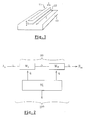
- An optical electro-absorption modulator (known under the acronym of EAM for electro-absorption modulator) is illustrated schematically in Figure 1.
- a modulator is well known per se in the state of technical. It is composed of a waveguide 11 produced in the form of a ribbon (mesa) on a substrate 10 in semiconductor material (from InP for example).
- the waveguide 11 has an active layer 12 in intrinsic semiconductor material framed by two layers of doped semiconductor material each of a different type of carriers.
- a control voltage is applied to the guide 11 to move the peak absorption of the waveguide 11 towards the wavelength working and allows for modulation amplitude of the wave passing through the guide.
- the width 1 of the waveguide 11 is fixed by the optical constraints of propagation of waves in guide 11.
- the thickness e of the active layer 12 is fixed by the constraints of manufacturing and more specifically by constraints epitaxy.
- the length L of the waveguide 11 can be reduced to decrease capacity C.
- a such decrease in length L will reduce absorption, reducing performance at the same time of the component.
- the purpose of the present invention is to solve the disadvantages mentioned, i.e. to reduce the capacity of a modulator without reducing its performance optics.
- the invention proposes to produce a optical transmitter comprising an electro-optical modulator consisting of a plurality of elements of modulation, each element having a guide length of reduced wave, therefore a capacity reduced by as much, and each controlled by the same electrical signal from ordered.
- the invention relates more specifically to a optical transmitter comprising an electro-optical modulator controlled by an electronic circuit of control, characterized in that said modulator includes N modulation elements comprising N separate and optically control electrodes coupled in series, and in that said circuit control electronics is capable of delivering N signals identical electrics on N separate outputs, each of the N outputs being connected respectively to each of the N control electrodes of the Depending on the application, the elements of modulation are electro-absorption modulators or Mach-Zender modulators.
- the circuit control electronics is a multiplexer or a amplifier with one or M inputs and N outputs synchronized.
- the transmitter optics is a monolithic integrated component.
- the electronic circuit is integrated into the electro-optical modulator.
- the objective of the present invention is to achieve an optical transmitter comprising an electro-optical modulator with the performance required for a high speed data transmission.
- the present invention therefore proposes to make a modulator made up of a plurality of modulation elements M N of reduced length, therefore of reduced capacity, and to place them optically in series in order to offset the disadvantage of the reduction in the absorption of l optical wave propagating in the modulator.
- the overall absorption of the optical wave emitted by the transmitter will be the sum of the absorptions in each of the modulation elements placed in series, while the bandwidth will be widened due to the decrease in the intrinsic capacity of each element. .
- FIG. 2 The implementation of the invention is illustrated diagrammatically in FIG. 2. An example is given with two modulation elements M 1 and M 2 , but the invention applies in the same way to N modulation elements arranged in series .
- a transmitter 100 such as a laser, must transmit, from a continuous source of wavelength ⁇ c , a modulated optical signal S m .
- the transmitter 100 includes an electro-optical modulator 30 consisting of N (two in the example) modulation elements M N (M 1 , M 2 ) optically arranged in series.
- the modulation elements M N consist of electro-absorption modulators (EAM).
- EAM electro-absorption modulators
- MN modulation elements made up of discrete Mach-Zender modulators (MZ).
- An electrical control signal Q is applied to the waveguide of each modulation element M N.
- the electrical control signal Q must be identical for each modulation element M N with a delay granted to the delay of the light signal between the elements M N.
- the modulation elements M N of the modulator 30 are thus electrically arranged in parallel.
- the modulator 30 is controlled by an electronic circuit 50 at an input E and N synchronized outputs Q.
- a control circuit 50 is known in the prior art and can be easily carried out by a person skilled in the art. It can be for example a multiplexer with one input and N outputs, or an amplifier circuit receiving an electrical signal of low amplitude at input (0.4 Volt for example) is output N synchronized electrical signals of control Q (of 3 to 4 Volts for example).
- an amplifier circuit is described in the publication ECOC 2000, September 2000 Kunststoff, entitled “ Short optical pulse generation at 20 GHZ repetition rate using integrated laser - modulators - amplifier” by G. Martin, E. Vergnol, A. Carence , and A. Ramdane ”.
- the modulator 30 and the electronic control circuit 50 are integrated on the same integrated circuit chip.
- the modulator can be integrated into the transmitter 100.
- Such a monolithic integration of the optical component 100 makes it possible to avoid the problems of phase shift of the optical wave.
- Such a monolithic integration of the modulation elements M N with the transmitter is possible because each modulation element is controlled with the same parallel electrical signal, which allows a common ground electrode between the modulation elements and the transmitter.
- a modulator of length L and of capacity C has been replaced, according to the illustrated example of the invention, by 2 modulation elements M 1 and M 2 of length L / 2. It follows that the overall length of the modulator 30 is 2xL / 2, that is to say L, therefore that the absorption has not been penalized; and that the intrinsic capacity of the modulator M has been reduced to C / 2 by the series connection of these two modulation elements M 1 and M 2 , therefore that the bandwidth of the transmitter 100 has been widened.
Landscapes
- Physics & Mathematics (AREA)
- Nonlinear Science (AREA)
- Optics & Photonics (AREA)
- Chemical & Material Sciences (AREA)
- General Physics & Mathematics (AREA)
- Engineering & Computer Science (AREA)
- Nanotechnology (AREA)
- Life Sciences & Earth Sciences (AREA)
- Biophysics (AREA)
- Crystallography & Structural Chemistry (AREA)
- Optical Modulation, Optical Deflection, Nonlinear Optics, Optical Demodulation, Optical Logic Elements (AREA)
- Optical Communication System (AREA)
- Amplifiers (AREA)
- Semiconductor Lasers (AREA)
Abstract
Description
- la figure 1, déjà décrite, est un schéma d'un modulateur à électro-absorption connu de l'état de la technique ;
- la figure 2 illustre schématiquement la structure d'un émetteur optique selon la présente invention.
Claims (7)
- Emetteur optique (100) comprenant un modulateur électro-optique (30) contrôlé par un circuit électronique de commande (50), caractérisé en ce que ledit modulateur (30) comprend N éléments de modulation (MN) comportant N électrodes de commande distinctes et optiquement couplés en série, et en ce que ledit circuit électronique de commande (50) est apte à délivrer N signaux électriques identiques (Q) sur N sorties distinctes, chacune des N sorties étant reliée respectivement à chacune des N électrodes de commande des éléments de modulation (MN).
- Emetteur optique selon la revendication 1, caractérisé en ce que les éléments de modulation (MN) sont des modulateurs à électro-absorption (EAM).
- Emetteur optique selon la revendication 1, caractérisé en ce que les éléments de modulation (MN) sont des modulateurs Mach-Zender discrets (MZ).
- Emetteur optique selon la revendication 1, caractérisé en ce que le circuit électronique de commande (50) est un multiplexeur à M entrées et N sorties synchronisées.
- Emetteur optique selon la revendication 1, caractérisé en ce que le circuit électronique de commande (50) est un amplificateur à une entrée et N sorties synchronisées.
- Emetteur optique selon l'une quelconque des revendications précédentes, caractérisé en ce que l'émetteur optique est un composant intégré monolithique.
- Emetteur optique selon l'une quelconque des revendications précédentes, caractérisé en ce que le circuit électronique de commande est intégré au modulateur électro-optique.
Applications Claiming Priority (2)
| Application Number | Priority Date | Filing Date | Title |
|---|---|---|---|
| FR0105758 | 2001-04-27 | ||
| FR0105758A FR2824152B1 (fr) | 2001-04-27 | 2001-04-27 | Emetteur optique comprenant un modulateur compose d'une pluralite d'elements de modulation |
Publications (2)
| Publication Number | Publication Date |
|---|---|
| EP1253462A1 true EP1253462A1 (fr) | 2002-10-30 |
| EP1253462B1 EP1253462B1 (fr) | 2008-11-05 |
Family
ID=8862814
Family Applications (1)
| Application Number | Title | Priority Date | Filing Date |
|---|---|---|---|
| EP02291048A Expired - Lifetime EP1253462B1 (fr) | 2001-04-27 | 2002-04-25 | Emetteur optique comprenant un modulateur compose d'une pluralite d'éléments de modulation |
Country Status (7)
| Country | Link |
|---|---|
| US (1) | US20020159665A1 (fr) |
| EP (1) | EP1253462B1 (fr) |
| JP (1) | JP2002365596A (fr) |
| CN (1) | CN1453943A (fr) |
| AT (1) | ATE413626T1 (fr) |
| DE (1) | DE60229688D1 (fr) |
| FR (1) | FR2824152B1 (fr) |
Families Citing this family (5)
| Publication number | Priority date | Publication date | Assignee | Title |
|---|---|---|---|---|
| US6990256B2 (en) * | 2002-06-20 | 2006-01-24 | Triquint Technology Holding Co. | Segmented modulator for high-speed opto-electronics |
| US9018984B2 (en) | 2013-02-01 | 2015-04-28 | Stmicroelectronics S.R.L. | Driver for high speed electrical-optical modulator interface |
| JP2017009626A (ja) * | 2015-06-16 | 2017-01-12 | 日本オクラロ株式会社 | 光信号生成装置 |
| CN109557686B (zh) * | 2018-12-03 | 2022-03-01 | 武汉邮电科学研究院有限公司 | 一种用于提高消光比并降低驱动电压的系统 |
| US11838055B2 (en) * | 2021-01-22 | 2023-12-05 | Nokia Solutions And Networks Oy | Apparatus comprising serially connected electro-absorption modulators |
Citations (5)
| Publication number | Priority date | Publication date | Assignee | Title |
|---|---|---|---|---|
| US3827000A (en) * | 1972-02-01 | 1974-07-30 | Nippon Selfoc Co Ltd | Optical modulator |
| US4776657A (en) * | 1986-03-25 | 1988-10-11 | Tektronix, Inc. | Electro-optic phase shifter with reduced input capacitance |
| JPH02170142A (ja) * | 1988-12-23 | 1990-06-29 | Nec Corp | 導波形光制御デバイス及びその駆動方法 |
| JPH07234390A (ja) * | 1994-02-25 | 1995-09-05 | Hitachi Ltd | 高速光素子の実装法 |
| JP2000284241A (ja) * | 1999-03-30 | 2000-10-13 | Mitsubishi Electric Corp | 半導体レーザ装置 |
Family Cites Families (7)
| Publication number | Priority date | Publication date | Assignee | Title |
|---|---|---|---|---|
| US5394260A (en) * | 1992-02-03 | 1995-02-28 | Kokusai Denshin Denwa Kabushiki Kaisha | Optical pulse generator |
| US5278923A (en) * | 1992-09-02 | 1994-01-11 | Harmonic Lightwaves, Inc. | Cascaded optical modulation system with high linearity |
| US5347601A (en) * | 1993-03-29 | 1994-09-13 | United Technologies Corporation | Integrated optical receiver/transmitter |
| SE507376C2 (sv) * | 1996-09-04 | 1998-05-18 | Ericsson Telefon Ab L M | Våglängdsavstämbar laseranordning |
| JP3681865B2 (ja) * | 1997-03-31 | 2005-08-10 | 三菱電機株式会社 | 光パルス位置検出回路及び光パルス位置検出方法 |
| JP3810570B2 (ja) * | 1998-12-24 | 2006-08-16 | アンリツ株式会社 | 光パルス発生方法及びその装置 |
| GB2375614B (en) * | 2000-04-06 | 2003-07-16 | Bookham Technology Plc | Optical modulator with pre-determined frequency chirp |
-
2001
- 2001-04-27 FR FR0105758A patent/FR2824152B1/fr not_active Expired - Fee Related
-
2002
- 2002-04-25 DE DE60229688T patent/DE60229688D1/de not_active Expired - Lifetime
- 2002-04-25 AT AT02291048T patent/ATE413626T1/de not_active IP Right Cessation
- 2002-04-25 EP EP02291048A patent/EP1253462B1/fr not_active Expired - Lifetime
- 2002-04-25 JP JP2002123707A patent/JP2002365596A/ja not_active Withdrawn
- 2002-04-26 CN CN02118378A patent/CN1453943A/zh active Pending
- 2002-04-26 US US10/132,162 patent/US20020159665A1/en not_active Abandoned
Patent Citations (5)
| Publication number | Priority date | Publication date | Assignee | Title |
|---|---|---|---|---|
| US3827000A (en) * | 1972-02-01 | 1974-07-30 | Nippon Selfoc Co Ltd | Optical modulator |
| US4776657A (en) * | 1986-03-25 | 1988-10-11 | Tektronix, Inc. | Electro-optic phase shifter with reduced input capacitance |
| JPH02170142A (ja) * | 1988-12-23 | 1990-06-29 | Nec Corp | 導波形光制御デバイス及びその駆動方法 |
| JPH07234390A (ja) * | 1994-02-25 | 1995-09-05 | Hitachi Ltd | 高速光素子の実装法 |
| JP2000284241A (ja) * | 1999-03-30 | 2000-10-13 | Mitsubishi Electric Corp | 半導体レーザ装置 |
Non-Patent Citations (7)
| Title |
|---|
| LI G L ET AL: "ULTRAHIGH-SPEED TRAVELING-WAVE ELECTROABSORPTION MODULATOR-DESIGN AND ANALYSIS", IEEE TRANSACTIONS ON MICROWAVE THEORY AND TECHNIQUES, IEEE INC. NEW YORK, US, vol. 47, no. 7, July 1999 (1999-07-01), pages 1177 - 1183, XP000846021, ISSN: 0018-9480 * |
| MALYUTIN A A: "INTEGRATED OPTICAL ANALOGS OF CLASSICAL INTERFEROMETERS", SOVIET JOURNAL OF QUANTUM ELECTRONICS, AMERICAN INSTITUTE OF PHYSICS. WOODBURY, NY, US, vol. 18, no. 8, 1 August 1988 (1988-08-01), pages 1019 - 1021, XP000048535 * |
| MARTIN G ET AL: "Short optical pulse generation at 20 GHz repetition rate using integrated laser-modulators-amplifier", ECOC 2000. 26TH EUROPEAN CONFERENCE ON OPTICAL COMMUNICATION, PROCEEDINGS OF 26TH EUROPEAN CONFERENCE ON OPTICAL COMMUNICATION, MUNICH, GERMANY, 3-7 SEPT. 2000, 2000, Berlin, Germany, VDE Verlag, Germany, pages 53 - 55 vol.2, XP008006614, ISBN: 3-8007-2567-3 * |
| PATENT ABSTRACTS OF JAPAN vol. 014, no. 434 (P - 1107) 18 September 1990 (1990-09-18) * |
| PATENT ABSTRACTS OF JAPAN vol. 1996, no. 01 31 January 1996 (1996-01-31) * |
| PATENT ABSTRACTS OF JAPAN vol. 2000, no. 13 5 February 2001 (2001-02-05) * |
| TANAKA H ET AL: "OPTICAL SHORT PULSE GENERATION BY DOUBLE GATE OPERATION OF TANDEM CONNECTED ELECTROABSORPTION MODULATORS DRIVEN BY SINUSOIDAL VOLTAGES", ELECTRONICS LETTERS, IEE STEVENAGE, GB, vol. 29, no. 16, 5 August 1993 (1993-08-05), pages 1449 - 1451, XP000388437, ISSN: 0013-5194 * |
Also Published As
| Publication number | Publication date |
|---|---|
| FR2824152B1 (fr) | 2004-01-30 |
| CN1453943A (zh) | 2003-11-05 |
| ATE413626T1 (de) | 2008-11-15 |
| EP1253462B1 (fr) | 2008-11-05 |
| JP2002365596A (ja) | 2002-12-18 |
| US20020159665A1 (en) | 2002-10-31 |
| DE60229688D1 (de) | 2008-12-18 |
| FR2824152A1 (fr) | 2002-10-31 |
Similar Documents
| Publication | Publication Date | Title |
|---|---|---|
| EP0017571B1 (fr) | Modulateur d'intensité lumineuse en optique intégrée et circuit optique intégré comportant un tel modulateur | |
| EP1412814B1 (fr) | Modulateurs electro-optiques large bande | |
| FR2521737A1 (fr) | Dispositif optique bistable | |
| EP3650925A1 (fr) | Commutateur optoelectronique a interferometre de mach-zehnder | |
| FR2640771A1 (fr) | Dispositif de translation de frequence optique et modulateur utilisant un tel dispositif | |
| FR2598823A1 (fr) | Coupleur optoelectronique directionnel pour un signal de commande non polarise. | |
| FR2743234A1 (fr) | Demultiplexeur de longueurs d'onde | |
| EP1253462B1 (fr) | Emetteur optique comprenant un modulateur compose d'une pluralite d'éléments de modulation | |
| EP0099282B1 (fr) | Dispositif optique intégré modulateur indépendant de la polarisation incidente | |
| FR2749945A1 (fr) | Composant electrooptique | |
| EP4671854A1 (fr) | Modulateur electro-optique de mach-zehnder comportant une ligne coplanaire rf a transmission amelioree | |
| EP1011011A1 (fr) | Modulateur de type Mach-Zehnder présentant un taux d'extinction très élevé | |
| EP1233299A1 (fr) | Composant optique intégré monolithique comportant un modulateur et un transistor bipolaire à hétérojonction | |
| FR2785730A1 (fr) | Amplificateur optique a semi-conducteur a gain stabilise reglable et systeme optique utilisant un tel amplificateur | |
| EP0632309B1 (fr) | Generateur d'impulsions optiques | |
| EP1031172B1 (fr) | Realisation d'emetteurs hyperfrequences et applications aux radars et aux telecommunications | |
| EP0801467B1 (fr) | Amplificateur distribué adaptateur basse impédance pour émetteur optoélectronique de signaux hyperfréquences à trés large bande | |
| EP0671791A1 (fr) | Modulateur semiconducteur électro-optique et liaison optique incluant ce modulateur | |
| EP0805371A1 (fr) | Modulateur électro-optique à puits quantiques | |
| WO2008101844A9 (fr) | Procede de commande d'un composant optique ou electro-optique et composant obtenu selon ce procede | |
| WO2006084999A1 (fr) | Modulateur a guide d’onde et procede de modulation associe | |
| FR3138219A1 (fr) | puce photonique pourvue d’un modulateur Mach-Zehnder | |
| EP0849620B1 (fr) | Modulateur électrooptique de faisceau lumineux | |
| EP0745232B1 (fr) | Modulateur electro-optique | |
| FR2858857A1 (fr) | Filtre commandable a commutation rapide |
Legal Events
| Date | Code | Title | Description |
|---|---|---|---|
| PUAI | Public reference made under article 153(3) epc to a published international application that has entered the european phase |
Free format text: ORIGINAL CODE: 0009012 |
|
| AK | Designated contracting states |
Kind code of ref document: A1 Designated state(s): AT BE CH CY DE DK ES FI FR GB GR IE IT LI LU MC NL PT SE TR |
|
| AX | Request for extension of the european patent |
Free format text: AL;LT;LV;MK;RO;SI |
|
| 17P | Request for examination filed |
Effective date: 20030502 |
|
| AKX | Designation fees paid |
Designated state(s): AT BE CH CY DE DK ES FI FR GB GR IE IT LI LU MC NL PT SE TR |
|
| RAP1 | Party data changed (applicant data changed or rights of an application transferred) |
Owner name: AVANEX CORPORATION |
|
| 17Q | First examination report despatched |
Effective date: 20070228 |
|
| GRAP | Despatch of communication of intention to grant a patent |
Free format text: ORIGINAL CODE: EPIDOSNIGR1 |
|
| GRAC | Information related to communication of intention to grant a patent modified |
Free format text: ORIGINAL CODE: EPIDOSCIGR1 |
|
| GRAS | Grant fee paid |
Free format text: ORIGINAL CODE: EPIDOSNIGR3 |
|
| GRAA | (expected) grant |
Free format text: ORIGINAL CODE: 0009210 |
|
| AK | Designated contracting states |
Kind code of ref document: B1 Designated state(s): AT BE CH CY DE DK ES FI FR GB GR IE IT LI LU MC NL PT SE TR |
|
| REG | Reference to a national code |
Ref country code: GB Ref legal event code: FG4D Free format text: NOT ENGLISH |
|
| REG | Reference to a national code |
Ref country code: CH Ref legal event code: EP |
|
| REG | Reference to a national code |
Ref country code: IE Ref legal event code: FG4D Free format text: LANGUAGE OF EP DOCUMENT: FRENCH |
|
| REF | Corresponds to: |
Ref document number: 60229688 Country of ref document: DE Date of ref document: 20081218 Kind code of ref document: P |
|
| NLV1 | Nl: lapsed or annulled due to failure to fulfill the requirements of art. 29p and 29m of the patents act | ||
| PG25 | Lapsed in a contracting state [announced via postgrant information from national office to epo] |
Ref country code: AT Free format text: LAPSE BECAUSE OF FAILURE TO SUBMIT A TRANSLATION OF THE DESCRIPTION OR TO PAY THE FEE WITHIN THE PRESCRIBED TIME-LIMIT Effective date: 20081105 Ref country code: ES Free format text: LAPSE BECAUSE OF FAILURE TO SUBMIT A TRANSLATION OF THE DESCRIPTION OR TO PAY THE FEE WITHIN THE PRESCRIBED TIME-LIMIT Effective date: 20090216 |
|
| PG25 | Lapsed in a contracting state [announced via postgrant information from national office to epo] |
Ref country code: NL Free format text: LAPSE BECAUSE OF FAILURE TO SUBMIT A TRANSLATION OF THE DESCRIPTION OR TO PAY THE FEE WITHIN THE PRESCRIBED TIME-LIMIT Effective date: 20081105 Ref country code: FI Free format text: LAPSE BECAUSE OF FAILURE TO SUBMIT A TRANSLATION OF THE DESCRIPTION OR TO PAY THE FEE WITHIN THE PRESCRIBED TIME-LIMIT Effective date: 20081105 |
|
| REG | Reference to a national code |
Ref country code: IE Ref legal event code: FD4D |
|
| PG25 | Lapsed in a contracting state [announced via postgrant information from national office to epo] |
Ref country code: DK Free format text: LAPSE BECAUSE OF FAILURE TO SUBMIT A TRANSLATION OF THE DESCRIPTION OR TO PAY THE FEE WITHIN THE PRESCRIBED TIME-LIMIT Effective date: 20081105 Ref country code: IE Free format text: LAPSE BECAUSE OF FAILURE TO SUBMIT A TRANSLATION OF THE DESCRIPTION OR TO PAY THE FEE WITHIN THE PRESCRIBED TIME-LIMIT Effective date: 20081105 |
|
| PG25 | Lapsed in a contracting state [announced via postgrant information from national office to epo] |
Ref country code: PT Free format text: LAPSE BECAUSE OF FAILURE TO SUBMIT A TRANSLATION OF THE DESCRIPTION OR TO PAY THE FEE WITHIN THE PRESCRIBED TIME-LIMIT Effective date: 20090406 Ref country code: SE Free format text: LAPSE BECAUSE OF FAILURE TO SUBMIT A TRANSLATION OF THE DESCRIPTION OR TO PAY THE FEE WITHIN THE PRESCRIBED TIME-LIMIT Effective date: 20090205 |
|
| PLBE | No opposition filed within time limit |
Free format text: ORIGINAL CODE: 0009261 |
|
| STAA | Information on the status of an ep patent application or granted ep patent |
Free format text: STATUS: NO OPPOSITION FILED WITHIN TIME LIMIT |
|
| 26N | No opposition filed |
Effective date: 20090806 |
|
| BERE | Be: lapsed |
Owner name: AVANEX CORP. Effective date: 20090430 |
|
| REG | Reference to a national code |
Ref country code: CH Ref legal event code: PL |
|
| PG25 | Lapsed in a contracting state [announced via postgrant information from national office to epo] |
Ref country code: LI Free format text: LAPSE BECAUSE OF NON-PAYMENT OF DUE FEES Effective date: 20090430 Ref country code: CH Free format text: LAPSE BECAUSE OF NON-PAYMENT OF DUE FEES Effective date: 20090430 |
|
| PG25 | Lapsed in a contracting state [announced via postgrant information from national office to epo] |
Ref country code: MC Free format text: LAPSE BECAUSE OF NON-PAYMENT OF DUE FEES Effective date: 20090430 |
|
| PG25 | Lapsed in a contracting state [announced via postgrant information from national office to epo] |
Ref country code: BE Free format text: LAPSE BECAUSE OF NON-PAYMENT OF DUE FEES Effective date: 20090430 |
|
| PG25 | Lapsed in a contracting state [announced via postgrant information from national office to epo] |
Ref country code: GR Free format text: LAPSE BECAUSE OF FAILURE TO SUBMIT A TRANSLATION OF THE DESCRIPTION OR TO PAY THE FEE WITHIN THE PRESCRIBED TIME-LIMIT Effective date: 20090206 |
|
| PG25 | Lapsed in a contracting state [announced via postgrant information from national office to epo] |
Ref country code: LU Free format text: LAPSE BECAUSE OF NON-PAYMENT OF DUE FEES Effective date: 20090425 |
|
| PG25 | Lapsed in a contracting state [announced via postgrant information from national office to epo] |
Ref country code: TR Free format text: LAPSE BECAUSE OF FAILURE TO SUBMIT A TRANSLATION OF THE DESCRIPTION OR TO PAY THE FEE WITHIN THE PRESCRIBED TIME-LIMIT Effective date: 20081105 |
|
| PG25 | Lapsed in a contracting state [announced via postgrant information from national office to epo] |
Ref country code: CY Free format text: LAPSE BECAUSE OF FAILURE TO SUBMIT A TRANSLATION OF THE DESCRIPTION OR TO PAY THE FEE WITHIN THE PRESCRIBED TIME-LIMIT Effective date: 20081105 |
|
| REG | Reference to a national code |
Ref country code: GB Ref legal event code: 732E Free format text: REGISTERED BETWEEN 20140612 AND 20140618 |
|
| REG | Reference to a national code |
Ref country code: FR Ref legal event code: CD Owner name: OCLARO (NORTH AMERICA), INC. Effective date: 20140930 |
|
| REG | Reference to a national code |
Ref country code: DE Ref legal event code: R081 Ref document number: 60229688 Country of ref document: DE Owner name: OCLARO (NORTH AMERICA), INC., FREMONT, US Free format text: FORMER OWNER: AVANEX CORP., FREMONT, CALIF., US Effective date: 20150218 |
|
| REG | Reference to a national code |
Ref country code: FR Ref legal event code: PLFP Year of fee payment: 15 |
|
| REG | Reference to a national code |
Ref country code: FR Ref legal event code: PLFP Year of fee payment: 16 |
|
| REG | Reference to a national code |
Ref country code: FR Ref legal event code: PLFP Year of fee payment: 17 |
|
| PGFP | Annual fee paid to national office [announced via postgrant information from national office to epo] |
Ref country code: DE Payment date: 20210426 Year of fee payment: 20 Ref country code: FR Payment date: 20210427 Year of fee payment: 20 Ref country code: IT Payment date: 20210428 Year of fee payment: 20 |
|
| PGFP | Annual fee paid to national office [announced via postgrant information from national office to epo] |
Ref country code: GB Payment date: 20210426 Year of fee payment: 20 |
|
| REG | Reference to a national code |
Ref country code: DE Ref legal event code: R071 Ref document number: 60229688 Country of ref document: DE |
|
| REG | Reference to a national code |
Ref country code: GB Ref legal event code: PE20 Expiry date: 20220424 |
|
| PG25 | Lapsed in a contracting state [announced via postgrant information from national office to epo] |
Ref country code: GB Free format text: LAPSE BECAUSE OF EXPIRATION OF PROTECTION Effective date: 20220424 |