EP1250032A1 - Electronic device using Zn-Al-Ge-Mg alloy solder having Al or Cu particles - Google Patents
Electronic device using Zn-Al-Ge-Mg alloy solder having Al or Cu particles Download PDFInfo
- Publication number
- EP1250032A1 EP1250032A1 EP02004434A EP02004434A EP1250032A1 EP 1250032 A1 EP1250032 A1 EP 1250032A1 EP 02004434 A EP02004434 A EP 02004434A EP 02004434 A EP02004434 A EP 02004434A EP 1250032 A1 EP1250032 A1 EP 1250032A1
- Authority
- EP
- European Patent Office
- Prior art keywords
- particles
- solder
- alloy
- bonding
- phase
- Prior art date
- Legal status (The legal status is an assumption and is not a legal conclusion. Google has not performed a legal analysis and makes no representation as to the accuracy of the status listed.)
- Granted
Links
Images


Classifications
-
- H—ELECTRICITY
- H10—SEMICONDUCTOR DEVICES; ELECTRIC SOLID-STATE DEVICES NOT OTHERWISE PROVIDED FOR
- H10W—GENERIC PACKAGES, INTERCONNECTIONS, CONNECTORS OR OTHER CONSTRUCTIONAL DETAILS OF DEVICES COVERED BY CLASS H10
- H10W72/00—Interconnections or connectors in packages
- H10W72/01—Manufacture or treatment
- H10W72/013—Manufacture or treatment of die-attach connectors
-
- B—PERFORMING OPERATIONS; TRANSPORTING
- B22—CASTING; POWDER METALLURGY
- B22F—WORKING METALLIC POWDER; MANUFACTURE OF ARTICLES FROM METALLIC POWDER; MAKING METALLIC POWDER; APPARATUS OR DEVICES SPECIALLY ADAPTED FOR METALLIC POWDER
- B22F1/00—Metallic powder; Treatment of metallic powder, e.g. to facilitate working or to improve properties
- B22F1/09—Mixtures of metallic powders
-
- B—PERFORMING OPERATIONS; TRANSPORTING
- B23—MACHINE TOOLS; METAL-WORKING NOT OTHERWISE PROVIDED FOR
- B23K—SOLDERING OR UNSOLDERING; WELDING; CLADDING OR PLATING BY SOLDERING OR WELDING; CUTTING BY APPLYING HEAT LOCALLY, e.g. FLAME CUTTING; WORKING BY LASER BEAM
- B23K1/00—Soldering, e.g. brazing, or unsoldering
- B23K1/0004—Resistance soldering
-
- B—PERFORMING OPERATIONS; TRANSPORTING
- B23—MACHINE TOOLS; METAL-WORKING NOT OTHERWISE PROVIDED FOR
- B23K—SOLDERING OR UNSOLDERING; WELDING; CLADDING OR PLATING BY SOLDERING OR WELDING; CUTTING BY APPLYING HEAT LOCALLY, e.g. FLAME CUTTING; WORKING BY LASER BEAM
- B23K35/00—Rods, electrodes, materials, or media, for use in soldering, welding, or cutting
- B23K35/02—Rods, electrodes, materials, or media, for use in soldering, welding, or cutting characterised by mechanical features, e.g. shape
- B23K35/0222—Rods, electrodes, materials, or media, for use in soldering, welding, or cutting characterised by mechanical features, e.g. shape for use in soldering or brazing
- B23K35/0244—Powders, particles or spheres; Preforms made therefrom
-
- B—PERFORMING OPERATIONS; TRANSPORTING
- B23—MACHINE TOOLS; METAL-WORKING NOT OTHERWISE PROVIDED FOR
- B23K—SOLDERING OR UNSOLDERING; WELDING; CLADDING OR PLATING BY SOLDERING OR WELDING; CUTTING BY APPLYING HEAT LOCALLY, e.g. FLAME CUTTING; WORKING BY LASER BEAM
- B23K35/00—Rods, electrodes, materials, or media, for use in soldering, welding, or cutting
- B23K35/22—Rods, electrodes, materials, or media, for use in soldering, welding, or cutting characterised by the composition or nature of the material
- B23K35/24—Selection of soldering or welding materials proper
- B23K35/28—Selection of soldering or welding materials proper with the principal constituent melting at less than 950°C
- B23K35/282—Zn as the principal constituent
-
- C—CHEMISTRY; METALLURGY
- C22—METALLURGY; FERROUS OR NON-FERROUS ALLOYS; TREATMENT OF ALLOYS OR NON-FERROUS METALS
- C22C—ALLOYS
- C22C18/00—Alloys based on zinc
-
- C—CHEMISTRY; METALLURGY
- C22—METALLURGY; FERROUS OR NON-FERROUS ALLOYS; TREATMENT OF ALLOYS OR NON-FERROUS METALS
- C22C—ALLOYS
- C22C18/00—Alloys based on zinc
- C22C18/04—Alloys based on zinc with aluminium as the next major constituent
-
- H—ELECTRICITY
- H10—SEMICONDUCTOR DEVICES; ELECTRIC SOLID-STATE DEVICES NOT OTHERWISE PROVIDED FOR
- H10W—GENERIC PACKAGES, INTERCONNECTIONS, CONNECTORS OR OTHER CONSTRUCTIONAL DETAILS OF DEVICES COVERED BY CLASS H10
- H10W72/00—Interconnections or connectors in packages
- H10W72/30—Die-attach connectors
-
- B—PERFORMING OPERATIONS; TRANSPORTING
- B23—MACHINE TOOLS; METAL-WORKING NOT OTHERWISE PROVIDED FOR
- B23K—SOLDERING OR UNSOLDERING; WELDING; CLADDING OR PLATING BY SOLDERING OR WELDING; CUTTING BY APPLYING HEAT LOCALLY, e.g. FLAME CUTTING; WORKING BY LASER BEAM
- B23K2101/00—Articles made by soldering, welding or cutting
- B23K2101/36—Electric or electronic devices
- B23K2101/40—Semiconductor devices
-
- H—ELECTRICITY
- H10—SEMICONDUCTOR DEVICES; ELECTRIC SOLID-STATE DEVICES NOT OTHERWISE PROVIDED FOR
- H10W—GENERIC PACKAGES, INTERCONNECTIONS, CONNECTORS OR OTHER CONSTRUCTIONAL DETAILS OF DEVICES COVERED BY CLASS H10
- H10W72/00—Interconnections or connectors in packages
- H10W72/071—Connecting or disconnecting
- H10W72/0711—Apparatus therefor
- H10W72/07125—Means for controlling the bonding environment, e.g. valves or vacuum pumps
-
- H—ELECTRICITY
- H10—SEMICONDUCTOR DEVICES; ELECTRIC SOLID-STATE DEVICES NOT OTHERWISE PROVIDED FOR
- H10W—GENERIC PACKAGES, INTERCONNECTIONS, CONNECTORS OR OTHER CONSTRUCTIONAL DETAILS OF DEVICES COVERED BY CLASS H10
- H10W72/00—Interconnections or connectors in packages
- H10W72/071—Connecting or disconnecting
- H10W72/0711—Apparatus therefor
- H10W72/07141—Means for applying energy, e.g. ovens or lasers
-
- H—ELECTRICITY
- H10—SEMICONDUCTOR DEVICES; ELECTRIC SOLID-STATE DEVICES NOT OTHERWISE PROVIDED FOR
- H10W—GENERIC PACKAGES, INTERCONNECTIONS, CONNECTORS OR OTHER CONSTRUCTIONAL DETAILS OF DEVICES COVERED BY CLASS H10
- H10W72/00—Interconnections or connectors in packages
- H10W72/071—Connecting or disconnecting
- H10W72/0711—Apparatus therefor
- H10W72/07178—Means for aligning
-
- H—ELECTRICITY
- H10—SEMICONDUCTOR DEVICES; ELECTRIC SOLID-STATE DEVICES NOT OTHERWISE PROVIDED FOR
- H10W—GENERIC PACKAGES, INTERCONNECTIONS, CONNECTORS OR OTHER CONSTRUCTIONAL DETAILS OF DEVICES COVERED BY CLASS H10
- H10W72/00—Interconnections or connectors in packages
- H10W72/071—Connecting or disconnecting
- H10W72/073—Connecting or disconnecting of die-attach connectors
-
- H—ELECTRICITY
- H10—SEMICONDUCTOR DEVICES; ELECTRIC SOLID-STATE DEVICES NOT OTHERWISE PROVIDED FOR
- H10W—GENERIC PACKAGES, INTERCONNECTIONS, CONNECTORS OR OTHER CONSTRUCTIONAL DETAILS OF DEVICES COVERED BY CLASS H10
- H10W72/00—Interconnections or connectors in packages
- H10W72/071—Connecting or disconnecting
- H10W72/073—Connecting or disconnecting of die-attach connectors
- H10W72/07331—Connecting techniques
- H10W72/07336—Soldering or alloying
-
- H—ELECTRICITY
- H10—SEMICONDUCTOR DEVICES; ELECTRIC SOLID-STATE DEVICES NOT OTHERWISE PROVIDED FOR
- H10W—GENERIC PACKAGES, INTERCONNECTIONS, CONNECTORS OR OTHER CONSTRUCTIONAL DETAILS OF DEVICES COVERED BY CLASS H10
- H10W72/00—Interconnections or connectors in packages
- H10W72/30—Die-attach connectors
- H10W72/321—Structures or relative sizes of die-attach connectors
- H10W72/325—Die-attach connectors having a filler embedded in a matrix
-
- H—ELECTRICITY
- H10—SEMICONDUCTOR DEVICES; ELECTRIC SOLID-STATE DEVICES NOT OTHERWISE PROVIDED FOR
- H10W—GENERIC PACKAGES, INTERCONNECTIONS, CONNECTORS OR OTHER CONSTRUCTIONAL DETAILS OF DEVICES COVERED BY CLASS H10
- H10W72/00—Interconnections or connectors in packages
- H10W72/30—Die-attach connectors
- H10W72/351—Materials of die-attach connectors
- H10W72/352—Materials of die-attach connectors comprising metals or metalloids, e.g. solders
-
- H—ELECTRICITY
- H10—SEMICONDUCTOR DEVICES; ELECTRIC SOLID-STATE DEVICES NOT OTHERWISE PROVIDED FOR
- H10W—GENERIC PACKAGES, INTERCONNECTIONS, CONNECTORS OR OTHER CONSTRUCTIONAL DETAILS OF DEVICES COVERED BY CLASS H10
- H10W72/00—Interconnections or connectors in packages
- H10W72/30—Die-attach connectors
- H10W72/351—Materials of die-attach connectors
- H10W72/353—Materials of die-attach connectors not comprising solid metals or solid metalloids, e.g. ceramics
- H10W72/354—Materials of die-attach connectors not comprising solid metals or solid metalloids, e.g. ceramics comprising polymers
-
- H—ELECTRICITY
- H10—SEMICONDUCTOR DEVICES; ELECTRIC SOLID-STATE DEVICES NOT OTHERWISE PROVIDED FOR
- H10W—GENERIC PACKAGES, INTERCONNECTIONS, CONNECTORS OR OTHER CONSTRUCTIONAL DETAILS OF DEVICES COVERED BY CLASS H10
- H10W72/00—Interconnections or connectors in packages
- H10W72/50—Bond wires
- H10W72/551—Materials of bond wires
- H10W72/552—Materials of bond wires comprising metals or metalloids, e.g. silver
- H10W72/5522—Materials of bond wires comprising metals or metalloids, e.g. silver comprising gold [Au]
-
- H—ELECTRICITY
- H10—SEMICONDUCTOR DEVICES; ELECTRIC SOLID-STATE DEVICES NOT OTHERWISE PROVIDED FOR
- H10W—GENERIC PACKAGES, INTERCONNECTIONS, CONNECTORS OR OTHER CONSTRUCTIONAL DETAILS OF DEVICES COVERED BY CLASS H10
- H10W72/00—Interconnections or connectors in packages
- H10W72/851—Dispositions of multiple connectors or interconnections
- H10W72/874—On different surfaces
- H10W72/884—Die-attach connectors and bond wires
-
- H—ELECTRICITY
- H10—SEMICONDUCTOR DEVICES; ELECTRIC SOLID-STATE DEVICES NOT OTHERWISE PROVIDED FOR
- H10W—GENERIC PACKAGES, INTERCONNECTIONS, CONNECTORS OR OTHER CONSTRUCTIONAL DETAILS OF DEVICES COVERED BY CLASS H10
- H10W74/00—Encapsulations, e.g. protective coatings
-
- H—ELECTRICITY
- H10—SEMICONDUCTOR DEVICES; ELECTRIC SOLID-STATE DEVICES NOT OTHERWISE PROVIDED FOR
- H10W—GENERIC PACKAGES, INTERCONNECTIONS, CONNECTORS OR OTHER CONSTRUCTIONAL DETAILS OF DEVICES COVERED BY CLASS H10
- H10W76/00—Containers; Fillings or auxiliary members therefor; Seals
- H10W76/10—Containers or parts thereof
- H10W76/17—Containers or parts thereof characterised by their materials
-
- H—ELECTRICITY
- H10—SEMICONDUCTOR DEVICES; ELECTRIC SOLID-STATE DEVICES NOT OTHERWISE PROVIDED FOR
- H10W—GENERIC PACKAGES, INTERCONNECTIONS, CONNECTORS OR OTHER CONSTRUCTIONAL DETAILS OF DEVICES COVERED BY CLASS H10
- H10W90/00—Package configurations
- H10W90/701—Package configurations characterised by the relative positions of pads or connectors relative to package parts
- H10W90/731—Package configurations characterised by the relative positions of pads or connectors relative to package parts of die-attach connectors
- H10W90/734—Package configurations characterised by the relative positions of pads or connectors relative to package parts of die-attach connectors between a chip and a stacked insulating package substrate, interposer or RDL
-
- H—ELECTRICITY
- H10—SEMICONDUCTOR DEVICES; ELECTRIC SOLID-STATE DEVICES NOT OTHERWISE PROVIDED FOR
- H10W—GENERIC PACKAGES, INTERCONNECTIONS, CONNECTORS OR OTHER CONSTRUCTIONAL DETAILS OF DEVICES COVERED BY CLASS H10
- H10W90/00—Package configurations
- H10W90/701—Package configurations characterised by the relative positions of pads or connectors relative to package parts
- H10W90/731—Package configurations characterised by the relative positions of pads or connectors relative to package parts of die-attach connectors
- H10W90/736—Package configurations characterised by the relative positions of pads or connectors relative to package parts of die-attach connectors between a chip and a stacked lead frame, conducting package substrate or heat sink
-
- H—ELECTRICITY
- H10—SEMICONDUCTOR DEVICES; ELECTRIC SOLID-STATE DEVICES NOT OTHERWISE PROVIDED FOR
- H10W—GENERIC PACKAGES, INTERCONNECTIONS, CONNECTORS OR OTHER CONSTRUCTIONAL DETAILS OF DEVICES COVERED BY CLASS H10
- H10W90/00—Package configurations
- H10W90/701—Package configurations characterised by the relative positions of pads or connectors relative to package parts
- H10W90/751—Package configurations characterised by the relative positions of pads or connectors relative to package parts of bond wires
- H10W90/754—Package configurations characterised by the relative positions of pads or connectors relative to package parts of bond wires between a chip and a stacked insulating package substrate, interposer or RDL
-
- H—ELECTRICITY
- H10—SEMICONDUCTOR DEVICES; ELECTRIC SOLID-STATE DEVICES NOT OTHERWISE PROVIDED FOR
- H10W—GENERIC PACKAGES, INTERCONNECTIONS, CONNECTORS OR OTHER CONSTRUCTIONAL DETAILS OF DEVICES COVERED BY CLASS H10
- H10W90/00—Package configurations
- H10W90/701—Package configurations characterised by the relative positions of pads or connectors relative to package parts
- H10W90/751—Package configurations characterised by the relative positions of pads or connectors relative to package parts of bond wires
- H10W90/756—Package configurations characterised by the relative positions of pads or connectors relative to package parts of bond wires between a chip and a stacked lead frame, conducting package substrate or heat sink
Definitions
- Sn-Pb alloy solders have made it possible to perform temperature-hierarchical bonding in which first soldering is performed at a temperature of about 330°C by use of a high-temperature solder such as Pb-rich Pb-5 mass% Sn (hereinafter the indication of "mass%" is omitted and only numerals are recited) solders (melting point: 314-310°C) or Pb-10Sn solders (melting point: 302-275°C) and in which second bonding is then performed by use of a low-melting point solder of Sn-37Pb eutectic (melting point: 183°C) without melting the first soldered portions.
- a high-temperature solder such as Pb-rich Pb-5 mass% Sn (hereinafter the indication of "mass%" is omitted and only numerals are recited) solders (melting point: 314-310°C) or Pb-10Sn solders (melting point: 302-275°C
- solders are soft and rich in deformability and, therefore, they can be used for bonding Si chips etc. apt to be broken to a substrate having a different thermal expansion coefficient and also for structural purposes.
- This temperature-hierarchical bonding is mainly adopted in semiconductor devices in which chips are die-bonded and in semiconductor devices in which chips are flip-chip-bonded such as BGA and CSP etc. In other words, this means that a solder used within a semiconductor device and another solder for bonding the semiconductor device itself to a substrate are used for the temperature-hierarchical bonding.
- the temperature-hierarchical bonding is used also for bonding power modules etc. used at high temperatures.
- the present invention relates to a Zn-Al alloy solder and a product in which this solder is used. More particularly, the invention relates to a Pb-free solder which makes it possible to perform temperature-hierarchical bonding on the high-temperature side relative to, for example, an Sn-Ag-Cu alloy Pb-free solder and which is a thermal-fatigue-resistant solder excellent in rolling workability, and a product in which the solder is used, such as, for example, a semiconductor device and a semiconductor module.
- Sn-Ag eutectic solders (melting point: 221°C), Sn-Ag-Cu eutectic solders (melting point: 221-217°C) and Sn-Cu eutectic solders (melting point: 227°C) come to be used.
- soldering temperatures in surface mounting be low in view of the heat resistance of parts, it is necessary to ensure wettability in order to keep the reliability and, for this reason, actual soldering temperatures in the case of the Sn-Ag-Cu eutectic solders capable of bonding at the lowest temperatures among Pb-free solders are about 235 to 250°C maximum in consideration of temperature variations within a substrate even if a furnace excellent in controlling for even temperature distribution is used. Therefore, solders capable of withstanding this soldering temperature range are required to have a melting point not less than 260°C.
- an Au-20Sn solder (melting point: 280°C) is known as a high-temperature solder, its use is limited to a narrow range because it is a hard material and its cost is high. Especially, in bonding an Si chip to a material having a different coefficient of thermal expansion or in bonding a large-size Si chip, this Au-20Sn solder is not used because there occurs such a fear as the Si chips are broken due to the high hardness of this solder.
- a material, a system and a structure which are suitable for large-area bonding for example, Si die-bonding and power module bonding.
- large-area bonding are required soft solder joints which have a thermal fatigue-resisting property and which are free from voids.
- flux-less bonding be possible when forming these joints.
- the object of the invention is to provide a new solder by improving and modifying Zn-Al alloy solders which new solder is used as the solder of the high-temperature side.
- This solder is intended to be used not only in the field of electronic devices, but also in the general structural field.
- an electronic device comprising at least one electronic part and a substrate on which the electronic part is mounted, the electronic part and the substrate being bonded to each other by joints comprising Al particles and an Al-Mg-Ge-Zn alloy, and the Al particles being connected to each other by the Al-Mg-Ge-Zn alloy.
- each of pads of the semiconductor chip and each of leads of a substrate on which the semiconductor chip is mounted are electrically connected by a gold wire, the semiconductor chip and the substrate being bonded by solder joints each comprising Al particles and an Al-Mg-Ge-Zn alloy.
- each of pads of the semiconductor chip and each of leads of a substrate on which the semiconductor chip is mounted are electrically connected by a gold wire, the semiconductor chip and the substrate being bonded by solder joints each comprising Cu particles and an Al-Mg-Ge-Zn alloy.
- the surfaces of the Al particles may be plated with at least one kind selected from the group consisting of Ni, Cu, Ag, Sn and Au.
- the surfaces of the Cu particles may plated with at least one kind selected from the group consisting of Ni, Cu, Ag, Sn and Au.
- each of the solder joints may include plastic particles.
- the material for the plastic particles may be made of at least one resin selected from the group consisting of polyimide, heat-resistant epoxy, silicone, various types of polymer beads, modified types of these materials and a mixture of these.
- each of the solder joints may have Sn and/or In particles in addition to the Al particles. This results in a reduction in the coefficient of thermal expansion of a solder.
- each of the solder joints may have Sn and/or In particles in addition to the Cu particles. This results in a reduction in the coefficient of thermal expansion of a solder.
- each of the solder joints may include particles of at least one kind selected from the group consisting of invar, silica, alumina, AlN and SiC in addition to the Al particles.
- AlN is aluminum nitride which is known as a high-thermal conductivity ceramic.
- SiC is silicon carbide which is known similarly as a high-thermal conductivity ceramic.
- each of the solder joints may include particles of at least one kind selected from the group consisting of invar, silica, alumina, AlN and SiC in addition to the Cu particles. This results in a reduction in the coefficient of thermal expansion of the solder.
- the Al-Mg-Ge-Zn alloy may consist, by mass, of 3 to 7% Al, 0.5 to 6% Mg, 1 to 5% Ge, and the balance Zn and incidental impurities.
- the Al-Mg-Ge-Zn alloy may include a 4Al-3Mg-4Ge-Zn alloy.
- an electronic device such as, for example, a semiconductor module or a multi-chip module, in which the semiconductor device is mounted on another circuit board by use of a Pb-free solder (, that is, a solder which does not positively contain any lead) such as an Sn-Ag-Cu alloy solder and etc.
- a Pb-free solder that is, a solder which does not positively contain any lead
- Sn-Ag-Cu alloy solder solder and etc.
- temperature-hierarchical (, that is, high-temperature and low-temperature) bonding can be realized for the Pb-free solder bonding of the semiconductor device (package) and for the mounting of the semiconductor device on another substrate.
- a method of producing a semiconductor device comprising the steps of: dicing a semiconductor wafer; mounting on a lead frame a chip cut from the semiconductor wafer (die-bonding); wire-bonding the semiconductor chip and the lead frame together by means of a gold wire etc.; resin-molding the semiconductor chip; and cutting the lead frame, wherein the semiconductor chip is mounted on the lead frame by use of a solder comprising Al particles and an Al-Mg-Ge-Zn alloy, and the Al particles are connected to each other by the Al-Mg-Ge-Zn alloy.
- a method of producing a semiconductor device comprising the steps of: dicing a semiconductor wafer; mounting on a lead frame a chip cut from the semiconductor wafer (die-bonding); wire-bonding the semiconductor chip and the lead frame together by means of a gold wire etc.; resin-molding the semiconductor chip; and cutting the lead frame, wherein the semiconductor chip is mounted on the lead frame by use of a solder comprising Cu particles or Cu particles subjected to a surface treatment such as Ni/Au plating and an Al-Mg-Ge-Zn alloy, and the Cu particles or surface-treated Cu particles are connected to each other by the Al-Mg-Ge-Zn alloy.
- the die-bonding may be performed while jetting a nitrogen gas.
- the die-bonding step of the semiconductor device manufacturing method may be performed in an inactive atmosphere of a nitrogen gas etc. or in a reducing atmosphere of a hydrogen gas etc. or in a mixed atmosphere of both of them.
- a semiconductor module or multi-chip module manufacturing method having the steps of mounting the semiconductor device on another substrate by use of a Pb-free solder such as an Sn-Ag-Cu alloy solder.
- the high-temperature side solder can, in most cases, withstand the process during the solder bonding for the post-bonding operation. That is, it is necessary that the high-temperature side solder which has already been bonded have a bonding strength capable of withstanding the reflow condition of 260°C. Accordingly, the present inventors have remarked Zn-Al alloy solders of a low cost as predominant high-temperature solders and have researched them for improving and reforming these solders.
- Some high-temperature solders used in power modules must have a melting point not less than 250°C and are, at the same time, required to meet such a severe condition as even a part of a solder must not melt, insofar as severe, some product fields are concerned. For this reason, the inventors have produced solders which do not melt even at temperatures not less than 260°C and other solder which have a strength even at 260°C even when they partly melt at this temperature.
- a Zn-5Al eutectic solder has a high melting point of 382°C and hence it is especially difficult to perform soldering at a relatively low temperature of about 300°C. In this case, it is necessary for the solder to have a composition which maintains a strength at a temperature not less than 260°C even when a part of the solder melts. Main requirements and problems are explained below and means for the solution thereof are described.
- the melting points of Zn-Al alloy solders must be lowered to a level of 300°C.
- the Zn-Al alloy solders must be rolling-workable.
- solder joints must have thermal fatigue-resisting properties; (4) the solder itself must have a flexibility; (5) in the state of a foil, the Zn-Al alloy solders must be free from voids; (6) it is possible to prevent the solders from being oxidized (soldering in a N 2 gas); and (7) the Zn-Al alloy solders must be excellent in corrosion resistance. Solders that can meet these requisites are suitable for the temperature-hierarchical bonding. Incidentally, it is not always necessary to meet all of these requisites.
- a Zn-Al alloy solder composition which has a melting point at a lowered level of 300°C and which is excellent in rolling-workability.
- a Zn-5AL solder is a eutectic solder having a melting point of 382°C, its melting point is too high and the solder poses the problem of oxidation.
- Mg is effective in preventing the grain-boundary corrosion and lowers the melting point, however, the Mg adding of an excessive amount makes the material brittle.
- the rolling working of a Zn-5Al-Mg alloy is impossible.
- the present inventors have found that the rolling working becomes possible when Ge is added to the Zn-5Al-Mg alloy.
- Ge is an element necessary for the rolling working.
- the workability of the Zn-5Al-Ge alloy itself is good, there are such problems as the melting point is too high and as the grain-boundary corrosion occurs. Accordingly, it is important to add both Mg and Ge in the Zn-Al alloy.
- the soldering temperature is decreased although the liquidus line temperature thereof does not decrease so much, with the result that the soldering at about 330°C becomes possible.
- the solderability thereof is improved by adding much amounts of Sn and In.
- the melting of an Sn-Zn phase (having a solidus line temperature of about 197°C) occurs.
- the melting of an In-Zn phase (having a solidus line temperature of about 144°C) occurs.
- the bonding can be performed at a temperature very close to 300°C and it become possible to keep a strength at the high temperature (, that is, in the case of an Sn-3Ag-0.5Cu alloy solder, the usual reflow temperature thereof becomes 250°C at maximum).
- the improvement in the thermal fatigue property (Paragraph 3) and the flexibility of the solder itself (Paragraph 4) can often be simultaneously achieved. That is, the Zn-Al-Mg-Ge alloy itself is hard in hardness and is poor in deformability although the solder has a high strength, a large rigidity and a good workability. Thus, in the case of using this solder for a large Si chip etc., there occurs such a fear as the fracture of the chip occurs. Therefore, by adding much amounts of In and Sn to improve the deformability and by dispersing the soft, pure Al particles of a high melting-point to soften the whole of the solder, it becomes possible to reduce the stress applied to the joints formed by the solder, so that the thermal fatigue properties can be improved.
- the aluminum and the Zn-Al-Mg-Ge alloy all prepared in the form of particles are mixed and dispersed to thereby prepare a powdered mixture.
- the mixture is then compacted and sintered under a static pressure in an inactive atmosphere or in a reducing atmosphere and are further rolled to thereby form a foil.
- a resulting structure is such that the Al particles become so-called "islands" and the Zn-Al-Mg-Ge particles having a low melting point becomes so-called "sea", that is, the Al particles come to be uniformly dispersed discretely and the space among the Al particles comes to be filled with the Zn-Al-Mg-Ge alloy phase which acts to connect the discrete Al particles to each other.
- the Zn-Al-Mg-Ge particles related to bonding be the "sea.”
- the surface of the Al particles may be plated with a thin coating of Ni/Au plating (, in which the Ni and Au layers are made to have such a thin thickness as to be 0.1 to 0.5 ⁇ m and 0.1 ⁇ m, respectively, and in this case the Ni may be diffused in the solder, that is, a thick layer of Ni deteriorates the deformability of the Al,) or with a thin coating of Ag plating etc.
- Ni/Au plating in which the Ni and Au layers are made to have such a thin thickness as to be 0.1 to 0.5 ⁇ m and 0.1 ⁇ m, respectively, and in this case the Ni may be diffused in the solder, that is, a thick layer of Ni deteriorates the deformability of the Al, or with a thin coating of Ag plating etc.
- fine plastic particles plated with Au may be dispersed in the solder. Also, by dispersing and mixing low-thermal-expansion particles which are metallized with a metal wettable through the solder or which are plated with an Sn alloy solder on the metallization layer, it is possible to relieve the stress and to thereby improve the thermal fatigue resisting property of the joints formed by the solder.
- the solder of the invention can clear high-temperature high-humidity test conditions (85°C, 85% RH, 1000 h) insofar as the Zn-Al-MG-Ge alloy solder is concerned.
- a rolled foil fabricated by mixing Zn-4Al-3Mg-4Ge particles and Al particles is described below.
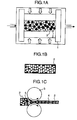
- FIG. 1A to Fig. 1C show schematic fabrication steps of a composite metal made of Zn-4Al-3Mg-4Ge alloy particles (melting point: 342-375°C, hardness: Hv 106) and pure Al particles (99.9%, hardness: Hv 17).
- FIG. 1A shows the state of the Al particles 2 and the Zn-4Al-3Mg-4Ge particles 3 contained in a carbon jig 1 of a vacuum hot press.
- FIG. 1B shows a cross-sectional model of the composite metal block obtained after the plastic flow of the solder portion which plastic flow occurs after a vacuum hot pressing, in which block the Zn-4Al-3Mg-4Ge particles are deformed to the "sea" 4 of the Zn-4Al-3Mg-4Ge alloy phase.
- FIG. 1C shows a model in which the composite ball block is further rolled by rolls 5 to thereby fabricate a solder foil.
- Zn-6Al-5Ge and Zn-20Al-3.5Ge alloys containing no Mg can be also rolled. Because the rolling-ability of the composite block of this composition is better than that of the composite block in the case where the composition contains a much amount of Al.
- Zn-4Al-3Mg-4Ge particles each having a size of 10 to 20 ⁇ m and Al particles of about 10 ⁇ m in size were mixed so that the Zn-4Al-3Mg-4Ge particles had a ratio of about 60 vol.%.
- Al particles it is possible to raise the packing ratio of the Al particles by further adding Al particle made to have smaller size so that the close-packed filling was able to be obtained.
- the Al particles have a large size, there occur unfavorable irregularities on the fillet surfaces of a joint, and hence it is preferred that the Al particles have a size of about 5 ⁇ m.
- the composite solder block made by use of this hot press was intended for use in the fabrication of the solder foil with a thickness of 150 ⁇ m, and in view of this it is preferred that the composite solder block be previously formed to have a thin shape close to the thickness of the foil so that a rolling operation can be readily performed because of a decreased rolling reduction needed to produce the foil.
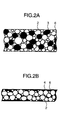
- Figs. 2A and 2B show a composite before and after the rolling thereof, in which composite, besides Al particles 2 and Zn-4Al-3Mg-4Ge particles 3, plastic particles (rubber) 6 each having a soft, elastic body metallized (by electroless Ni plating-Au plating, or Au plating, or electroless Ni plating-solder plating) are dispersed in order to further lower the Young's modulus thereof.
- the plating coating provided on the plastic particles be such a soft one as that of Au, or Ag, or Al etc. which is capable of mitigating stresses caused by a deformation.
- the function of the rubber can be maintained insofar as the plastic particles are present in the solder.
- the size of the resin particles is not more than 10 ⁇ m and preferably in the range of not more than 1 ⁇ m. As regards the amount of the plastic particles, even a few volume percents thereof is effective.
- the Zn-4Al-3Mg-4Ge alloy which is wettable regarding Al in a reducing or inactive atmosphere, it is not necessary to perform the metallization on the surface of the Al particles. However, performing Ni/Au plating, or Ni/Sn plating etc. is effective to further raise the bonding strength therebetween. Further, the surface of the Al particles may be coated with a thin coating of Au, or Ag etc. by sputtering etc. Since the Zn-4Al-3Mg-4Ge alloy is hard in hardness at a low temperatures, it is preferred that each of the Al particles be spherical in shape to minimize an energy loss occurring by contact friction etc. and to increase a damping property against impact and oscillation.
- the particles of the alloy and the Al particles can be mass-produced at a low cost through a conventional atomizing process.
- As a substitute for the Al particles it is also possible to use Cu, Ag or Au particles which have a high melting point and are relatively soft in hardness.
- compositions obtained from Zn-Al-based alloy solders which is capable of being rolling-worked there are a Zn-Al-Mg-Ga alloy (, for example, a Zn-4Al-3Mg-3Ga alloy), a Zn-Al-Ge alloy (, for example, a Zn-6Al-5Ge alloy and a Zn-20Al-3Ge alloy), a Zn-Al-Ge-Ga alloy (, for example, a Zn-6Al-5Ge-3Ga alloy), a Zn-Al-Mg-Ge alloy (, for example, a Zn-4Al-3Mg-4Ge alloy), a Zn-Al-Mg-Ge-Ga alloy (, for example, a Zn-4Al-1Mg-2Ge-3Ga alloy) and ones in which at least one kind selected from the group consisting of Sn, In, Ag, Cu, Au, Ni, Pd and etc.
- heat-resistant plastic particles plated with an Ni-Sn alloy or Au were uniformly dispersed in the Zn-Al alloy particles, whereby the Young's modulus of the solder was lowered.
- available solder particles are limited to the Zn-Al-Mg-Ge alloy and the Zn-Al-Mg-Ge-Ga alloy, both of which contain Mg and Ge. It is preferred that these plastic particles be fine in size in comparison with the size of the Zn-Al alloy particles and be dispersed substantially uniformly.
- the plastic particles of 1 ⁇ m level in size which are soft in hardness and which have elasticity are present at the time of the deformation, it becomes possible to obtain a remarkable relaxation against the thermal impact and against mechanical impact. That is, the rubber dispersed in the Zn-Al alloy solder particles acts to reduce the Young's modulus. Because the plastic particles are substantially uniformly dispersed among the Zn-Al alloy solder particles, this dispersion is not varied so much insofar as the melting thereof for a short period of time is concerned.
- These particles are mixed and put beforehand in a container having such a shape as to be readily rolling-worked to a foil, and they are compacted in a vacuum by hot-pressing. During the compacting, the particles are uniformly compressed at a temperature at which no melting of the plating coating of Sn provided on the plastic particles occurs (melting point of Sn: 232°C), whereby the plastic flow of the solder alloy particles occurs. Because the Zn-Al alloy particles is soft in hardness at a level of 220°C, that is, 8 Hv in hardness, the particles are easily deformed. A block in which the particles are substantially uniformly dispersed by the uniform compression is rolled to a thickness of about 150 ⁇ m to thereby fabricate a composite solder foil. When the foil is used in die bonding, it can be continuously supplied by use of a roll on which the foil is wound.
- the Zn-Al alloy solders are apt to be oxidized, it is preferred, in taking the storage thereof into consideration, that the surface thereof be plated with Sn. This Sn is dissolved in the Zn-Al alloy solders at the time of the die bonding. The presence of Sn on the surface of the solder facilitates, for example, the bonding to an Ni-Au plating coating provided on a Cu stem.
- a Si-chip can also be easily bonded to, for example, a Cr-Ni-Ag metallized surface.
- Sn particles or In particles may be further mixed in an amount of 10 to 30 vol.% so that the Sn or In particles are present among the Zn-Al alloy solder particles, with the result that a part of the Sn or In particles is dissolved in the Zn-Al alloy particles together, other portions coming to exist in the state of Sn or In phase, which is not precipitated nor dissolved, and in the state of a soft Sn-Zn or In-Zn phase of a low melting point.
- the deformation for relaxing the stress is brought about by the rubber of the plastic particles and the Sn, In, Sn-Zn or In-Zn phase.
- the solidus line temperatures of the Zn-Al alloy solders is kept to be not less than 280°C and, so that there is no problem regarding the strength at the high temperatures.
- this composition is intended for use in a hierarchical bonding performed at a relatively low temperature, so that the Sn, In, Sn-Zn or In-Zn phases is re-melted during the reflow.
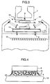
- FIG. 3 shows an example of a die bonding process in which a solder foil 11 is used.
- the process had the steps of: preparing a foil which was fabricated by mixing Zn-4Al-2Mg-3Ge-1Ag-10Sn particles, Al particles, a small amount of Sn particles, and solder-plated plastic particles; plating the foil with Sn (0.5 ⁇ m); placing the foil on a Cu stem 13 coated with Ni (3 ⁇ m)-Au (0.1 ⁇ m) layers; vacuum-sucking a Si chip 8 coated with a layer 38 of a Cr-Ni-Ag alloy which chip has a square shape with one side of 5 mm so that the Si chip is held on an electric resistance heating tool 7 of pulse-current; bringing the chip 8 into pressure-contact(initial pressure: 2 kgf) with the foil 11 having a square shape with one side of 4 mm and a thickness of 0.15 mm; and keeping them at a temperature of 400°C at maximum for 10 seconds.
- thermocouple 16 for measuring the temperature was embedded near a portion at which the tip of the tool comes to contact with the chip.
- the solder foil is instantaneously melted when the temperature thereof reaches to the melting point, there was provided means for keeping the heating tool at a level spaced downward by 20 ⁇ m from the position where the pressure-contact is commenced between the foil and the tool, so that the molten solder is prevented from being crushed flat during the heating.
- the preheating of the stem on the substrate side was performed at about 200°C, and in order to prevent the oxidation of the solder foil, nitrogen gas 10 was locally jetted from the surrounding onto the solder foil.
- nitrogen gas 10 was also fed to the surrounding of the tool adsorbing the Si chip 8 so that an oxygen concentration of 50 to 100 ppm level may be always maintained around the joint.
- the tool 7 adsorbing the Si chip in Fig. 3 has such a structure as to adsorb the surface of the chip, however, the tool is usually made to have such a structure as to apply a pressure onto the end portion of the chip so as to minimize a damage applied to the surface of the element.
- this foil it is possible to perform the reflow bonding of a power module etc. in a hydrogen gas furnace or in an inactive atmosphere furnace at a temperature of about 380°C at maximum.
- FIG. 4 shows a cross section of the Si chip bonded to the Cu stem.
- a metallization coating 42 on the Cu stem 13 there is used Ni-Ag, or Ag besides the Ni-Au.
- As another metallization coating provided on the Si chip it is possible to use Cr-Ni-Au, Ni-Au, Ni-Ag, or Ni-Sn etc.
- the Sn or In comes to be readily wetted and spread by raising the temperature to a level not less than the liquidus line temperatures of the Zn-Al-Mg-Ge alloy solder, so that Sn or In is dissolved in the Zn-Al-Mg-Ge alloy solder. If the amount of Sn or In is excessive, all of Sn or In cannot be dissolved in the Zn-AL-Mg-Ge alloy and comes to be precipitated as a low-melting point Sn-Zn phase or In-Zn phase at grain boundaries.
- the Sn-Zn or In-Zn phase by intentionally making much Sn or In phases dispersed and precipitated, it is possible for the Sn-Zn or In-Zn phase to bear the deformation and for the Zn-Al alloy phase to bear the bonding strength. Accordingly, by plating the Zn-Al-Mg-Ge alloy particles with Sn or In and by intentionally making the Sn or In phases remain which cannot exist in a solid solution state in the Zn-AL-Mg-Ge particles, the deformation can be made to be absorbed by the Sn or In phase, whereby it is possible to lessen the rigidity of the solder.
- plastic particles each having a size of about 1 ⁇ m each of which particles is coated with the alloy solder may be contained in the composite solder, so that the impact-resistance of the composite solder and the Young's modulus thereof can be improved.
- the thermal fatigue resisting property of joints formed of this solder is improved.
- Sn or In may be added by plating each of the Zn-AL-Mg-Ge alloy particles with Sn or In or by adding and dispersing Sn or In particles of an appropriate amount, so that these particles containing Sn or In or the Sn or In particles may plastically flow among the Zn-Al-Mg-Ge alloy solder particles in a vacuum. Since the simple substance phase of Sn and In is softer in hardness than the low-melting point phase of the Zn-Sn or Zn-In alloy, the latter case is preferred in the view point of coping with a deformation.
- the composite foil fabricated in the process according to the embodiment can be continuously supplied by use of a reel on which the foil is wound, the cutting thereof step being also performed continuously.
- the sealing portion and terminal joint of a part in which a temperature-hiererchical bonding is required it is possible to perform the bonding of flux-less type by the steps of preparing, by punching etc., a solder foil having a shape corresponding to a solder joint to be formed, locating and fixing the punched foil on a substrate or on a part, applying and heating the foil in a nitrogen gas atmosphere by use of a pulse type pressurizing-and-heating tool.
- a foil plated with Sn in order to ensure the prevention of the oxidation during the preheating and to keep the wettability.
- Fig. 5A shows a cross section of a ceramic BGA or CSP produced by the steps of; locating a foil according to each of Embodiments 1 to 3 on an interchange substrate 36; applying a pressure to a chip 8 after sucking it by use of a tip tool having an electric resistance heating body for pulse-heating; performing the die-bonding shown by the reference numeral 39; connecting terminals on the chip and terminals on the interchange substrate 36 to each other by wire-bonding through Au wires 35; locating another foil according to each of Embodiments 1 to 3 between a fin 23 of Ni-Au plated Al etc. and the interchange substrate; and performing the sealing 25 of a fluxless type in a nitrogen gas atmosphere by use of the resistance heating body to thereby obtain the ceramic BGA or CSP.
- the process can also be applied to the mounting of a module in which resistors and capacitors are mounted on a chip.
- a joint is formed of a composite solder superior in thermal conduction which contains aluminum, it is possible to provide a good heat dissipation toward the interchange substrate superior in thermal conduction.
- FIG. 5B-1 shows a punched piece of foil 40 which is similarly fabricated from a material containing the Zn-Al-Mg-Ge particles and the Al particles according to each of the Embodiments 1 to 3.
- FIG. 5B-2 shows a cross-section of a model of heating the foil 40 and the Al fin 23 by use of a heating-and-pressurizing body 41 of a pulse heating type in a nitrogen gas atmosphere.
- a heating-and-pressurizing body 41 of a pulse heating type in a nitrogen gas atmosphere.
- main bonding in the hydrogen gas furnace after the tack soldering of the foil 40 at 400°C for 5 seconds performed by means of the pressurizing-and-heating body 41.
- FIG. 5C shows a sectional model of the composite solder foil in which an Sn plating layer 17 encloses the periphery of the composite solder foil 11.
- FIG. 6A is a plan view of a package in which a lead frame 18 and a thermal dissipation plate 19 are positioned, bonded and caulked to each other, in which there are two caulking portions 20.
- the interconnection terminals on the chip and leads 18 are wire-bonded 35 and resin molded 21.
- FIG. 6B is a cross-sectional view of the package and
- FIG. 6C is a partially enlarged view of a portion of the package.
- Heat occurring from a heat-generating chip 8 of about 3W level is conducted through a solder 47 to a thermal diffusion plate 19(made of a Cu-based low-expansion composite material) of a header.
- the solder that smoothly dissipates the heat generated in the high-output chip toward the thermal diffusion plate has a great role, and a remarkable improvement in the heat dissipation can be brought about from the composite solder according to the embodiments 1 to 3 containing the Al particles phase excellent in thermal conductivity and the Zn-Al alloy solder phase, in comparison with conventional Pb alloy solders.
- FIG. 7 shows the fabrication process of a package.
- the lead material was made of a 42 Alloy (, that is, 42 Ni-Fe alloy). After the dam cutting but before lead cutting thereof, a Sn alloy solder plating was applied to the lead material.
- the pads on the rear face of an Si chip 8 (Fig. 6C) were coated with a thin film of a Cr-Ni-Au, Cr-Ni-Ag, Ti-Ni-Ag or Ti-Ni-Au alloy etc. or with a Ni-Ag plating etc.
- the die bonding of the chip was performed by means of a pulse resistance heating body under an initial pressure of 2 kgf at 400°C for 10 seconds while jetting a nitrogen gas thereto.
- the heating body was set to stop at a position 20 ⁇ m spaced below from the initially pressure-applying position (, that is, a solder thickness of 150 ⁇ m) thereby to ensure a constant solder thickness, so that a constant thickness of the solder joint was obtained.
- the reduction in the void ratio of the joint is important, and an intended void ratio not more than 5% was able to be achieved in this embodiment. Since the solder contains the Al particles, the solder will not move freely at the time of the bonding, so that voids are less apt to occur.
- the joint formed of the solder displayed good characteristics because of the flexibility thereof brought about by the Al particles. Since the solidus line temperature of the solder is not less than 300°C, the solder ensures a high reliability even at a high temperature of about 260°C.
- the chip was resin-molded 21 (Fig. 6C), and the dam cutting 14 (Fig. 6A)was performed. Then, an Sn-Bi alloy Pb-free solder was applied to the lead 18 so that a coating having a thickness of 2 to 8 ⁇ m was provided thereon. After that, the lead was cut and formed and unneeded potions in the thermal dissipation plate were cut, whereby the package was completed.
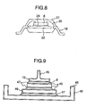
- FIG. 8 shows an example in which the composite solder according to each of Embodiments 1 to 3 is applied to a usual plastic package.
- the rear face of an Si chip 8 is bonded onto a tab 22 of 42 Alloy through an electrically conductive joint 24 made of this solder.
- the Si chip is bonded to a lead 18 by wire-bonding 35 and is then resin-molded 21.
- a Sn-Bi alloy Pb-free solder was applied to the lead.
- this solder foil to the plastic packages is effective in all package structures in each of which a Si chip and a tab are bonded to each other. Regarding the structure, these packages are sorted into a gull wing type, a flat type, a J-lead type, a butt-lead type, a lead-less type and etc.
- FIG. 9 shows an example in which a solder foil relating to the invention was applied to the bonding of a power module.
- a diode Si chip 8 is often made to have a size of 6.5 mm.
- soft Pb-rich high-temperature solders have been used.
- the foil made of a mixture of Zn-6Al-5Ge alloy particles excellent in rolling-ability and Al particles was used.
- the Zn-6Al-5Ge alloy particles of 5 to 10 ⁇ m and the Al particles of 5 to 10 ⁇ m were mixed at a weight ratio of about 1:1, the mixture being subjected to a hot pressing operation in a vacuum or in a reducing atmosphere so that the Zn-6Al-5Ge alloy particles was made to plastically flow among the Al particles, and the composite material was rolling-worked to thereby produce a solder foil.
- This solder foil was cut to a predetermined size and was placed between the Si chip 8 and a low-thermal-expansion substrate 46 made of a Ni-plated Mo plate or made of a composite of both of invar and Cu, the solder foil being also placed between the substrate 46 and a Ni-plated Cu plate 49, the solder foil being further placed between the Si chip 8 and a Cu electrode terminal 12 having a Ni-plating coating 45, and these components were reflow-bonded at a time in a hydrogen gas furnace at 400°C. It was confirmed that, by performing a temperature cycle test and a power cycle test regarding the power module thus formed, the joint provided in this embodiment had a service life equivalent to that of joints provided by use of conventional Pb-containing solders.
- the Young's module of the joint can be lowered with the result that thermal impact resisting property of the joint can be further improved, making it possible to successfully perform the bonding of a larger size Si chip.
- the bonding by use of the solder relating to the invention is not limited to the mounting of the electronic device, but is applicable to the bonding or sealing etc. of a structural member because the solder has an excellent, low elasticity, whereby the reliability can be remarkably improved and the application thereof in various fields can be expected.
Landscapes
- Engineering & Computer Science (AREA)
- Mechanical Engineering (AREA)
- Chemical & Material Sciences (AREA)
- Materials Engineering (AREA)
- Metallurgy (AREA)
- Organic Chemistry (AREA)
- Die Bonding (AREA)
- Electric Connection Of Electric Components To Printed Circuits (AREA)
Abstract
Description
Claims (11)
- An electronic device comprising at least one electronic part (8) and a substrate (13, 22, 36, 46) on which said electronic part is mounted, said electronic part and said substrate being bonded by a joint (24, 39, 47) comprising a phase of Al particles (2) and another phase of an Al-Mg-Ge-Zn alloy (4), said Al particles being connected to each other by said Al-Mg-Ge-Zn alloy phase.
- A semiconductor device comprising a semiconductor chip (8), electrode pads provided on said semiconductor chip, a substrate (22) on which said semiconductor chip is mounted, a lead (18) of said substrate which lead is electrically connected to said electrode pads through a gold wire (35), and a solder joint (24), said semiconductor chip and said substrate being bonded by said solder joint comprising a phase of Al particles (2) and another phase of an Al-Mg-Ge-Zn alloy (4).
- A semiconductor device comprising a semiconductor chip (8), electrode pads provided on said semiconductor chip, a substrate (22) on which said semiconductor chip is mounted, a lead (18) of said substrate which lead is electrically connected to said electrode pads through a gold wire (35), and a solder joint (24, 39), said semiconductor chip and said substrate being bonded by said solder joint comprising a phase of Cu particles and another phase of an Al-Mg-Ge-Zn alloy (4).
- The device of claim 2, wherein the surface of each of said Al particles is plated with Ni, Cu, Ag, Sn and/or Au.
- The device of claim 3, wherein the surface of each of said Cu particles is plated with Ni, Cu, Ag, Sn and/or Au.
- The device of claim 2 or 3, wherein said solder joints further have a third phase of particles (6) of a plastic.
- The device of claim 6, wherein said plastic particles (6) are made of a polyimide, a heat-resistant epoxy, a silicone, various types of polymer beads, modified types of these, or a mixture of these.
- The device of claim 2, wherein said solder joint further includes, in addition to the phase of said Al particles (2), Sn particles, In particles, invar particles, silica particles, alumina particles, AlN particles and/or SiC particles.
- The device of claim 3, wherein said solder joint further includes, in addition to the phase of said Cu particles, Sn particles, In particles, invar particles, silica particles, alumina particles, AlN particles and/or SiC particles.
- The device of claim 2 or 3, wherein said Al-Mg-Ge-Zn alloy (4) consists, by mass, of 3 to 7 % Al, 0.5 to 6 % Mg, 1 to 5 % Ge, and the balance Zn and incidental impurities.
- The device of claim 2 or 3, wherein said Al-Mg-Ge-Zn alloy (4) includes a 4 mass%Al-3 mass%Mg-4 mass%Ge-the balance Zn alloy.
Applications Claiming Priority (2)
| Application Number | Priority Date | Filing Date | Title |
|---|---|---|---|
| JP2001112157 | 2001-04-11 | ||
| JP2001112157A JP3800977B2 (en) | 2001-04-11 | 2001-04-11 | Products using Zn-Al solder |
Publications (2)
| Publication Number | Publication Date |
|---|---|
| EP1250032A1 true EP1250032A1 (en) | 2002-10-16 |
| EP1250032B1 EP1250032B1 (en) | 2006-04-26 |
Family
ID=18963618
Family Applications (1)
| Application Number | Title | Priority Date | Filing Date |
|---|---|---|---|
| EP02004434A Expired - Lifetime EP1250032B1 (en) | 2001-04-11 | 2002-02-26 | Electronic device using Zn-Al-Ge-Mg alloy solder having Al or Cu particles |
Country Status (4)
| Country | Link |
|---|---|
| US (1) | US6563225B2 (en) |
| EP (1) | EP1250032B1 (en) |
| JP (1) | JP3800977B2 (en) |
| DE (1) | DE60210858T2 (en) |
Cited By (7)
| Publication number | Priority date | Publication date | Assignee | Title |
|---|---|---|---|---|
| WO2007085563A1 (en) * | 2006-01-25 | 2007-08-02 | Robert Bosch Gmbh | Method of applying a solder deposit consisting of a solder material to a substrate by cold gas spraying, and powdery solder material, wherein the solder material contains powdery soft solder and powdery aluminium |
| CN101653878B (en) * | 2009-09-11 | 2011-07-27 | 北京工业大学 | Zn-Mg magnesium alloy solder |
| CN102814596A (en) * | 2011-06-07 | 2012-12-12 | 英飞凌科技股份有限公司 | Solder alloys and arrangements |
| CN106536108A (en) * | 2014-04-17 | 2017-03-22 | 贺利氏材料新加坡私人有限公司 | Lead-free eutectic solder alloy containing zinc as main component and aluminum as alloy metal |
| EP3077151A4 (en) * | 2013-12-04 | 2017-09-27 | Honeywell International Inc. | Zinc-based lead-free solder compositions |
| CN110891732A (en) * | 2017-05-15 | 2020-03-17 | 法尔冲压技术有限责任公司 | Lead-free solder film for diffusion soldering and method for the production thereof |
| EP3627546B1 (en) * | 2018-09-24 | 2024-10-30 | Infineon Technologies AG | Power semiconductor module arrangement |
Families Citing this family (94)
| Publication number | Priority date | Publication date | Assignee | Title |
|---|---|---|---|---|
| KR100548114B1 (en) * | 2000-12-21 | 2006-02-02 | 가부시키가이샤 히타치세이사쿠쇼 | Solder foil and semiconductor devices and electronic devices |
| JP4684439B2 (en) * | 2001-03-06 | 2011-05-18 | 富士通株式会社 | Conductive particles, conductive composition, and method for manufacturing electronic device |
| JP2003234433A (en) * | 2001-10-01 | 2003-08-22 | Matsushita Electric Ind Co Ltd | Semiconductor device, method of mounting semiconductor device, and package and method of manufacturing the same |
| US7846778B2 (en) * | 2002-02-08 | 2010-12-07 | Intel Corporation | Integrated heat spreader, heat sink or heat pipe with pre-attached phase change thermal interface material and method of making an electronic assembly |
| US7473995B2 (en) * | 2002-03-25 | 2009-01-06 | Intel Corporation | Integrated heat spreader, heat sink or heat pipe with pre-attached phase change thermal interface material and method of making an electronic assembly |
| JP3509809B2 (en) * | 2002-04-30 | 2004-03-22 | 住友電気工業株式会社 | Submount and semiconductor device |
| US20040007780A1 (en) * | 2002-07-09 | 2004-01-15 | Hundt Paul Joseph | Particle-filled semiconductor attachment material |
| US7199305B2 (en) * | 2002-08-08 | 2007-04-03 | Nanoink, Inc. | Protosubstrates |
| JP4537019B2 (en) * | 2003-06-04 | 2010-09-01 | 古河スカイ株式会社 | Brazing method of aluminum material |
| DE10335111B4 (en) * | 2003-07-31 | 2006-12-28 | Infineon Technologies Ag | Assembly method for a semiconductor device |
| JP2005095977A (en) * | 2003-08-26 | 2005-04-14 | Sanyo Electric Co Ltd | Circuit equipment |
| JP4130167B2 (en) * | 2003-10-06 | 2008-08-06 | 日東電工株式会社 | Semiconductor wafer peeling method |
| JP4130407B2 (en) * | 2003-12-26 | 2008-08-06 | 株式会社東芝 | Electronic circuit manufacturing method |
| JP4524454B2 (en) * | 2004-11-19 | 2010-08-18 | ルネサスエレクトロニクス株式会社 | Electronic device and manufacturing method thereof |
| US20060120911A1 (en) * | 2004-12-08 | 2006-06-08 | Manoj Gupta | Method of forming composite solder by cold compaction and composite solder |
| JP4772320B2 (en) * | 2004-12-15 | 2011-09-14 | 富士通株式会社 | Zinc-aluminum solder alloy |
| KR100695116B1 (en) | 2004-12-27 | 2007-03-14 | 삼성전기주식회사 | Solder for Device Package |
| JP4344707B2 (en) * | 2005-02-24 | 2009-10-14 | 株式会社ルネサステクノロジ | Semiconductor device and manufacturing method thereof |
| JP4891556B2 (en) * | 2005-03-24 | 2012-03-07 | 株式会社東芝 | Manufacturing method of semiconductor device |
| JP2007073681A (en) * | 2005-09-06 | 2007-03-22 | Renesas Technology Corp | Semiconductor device and manufacturing method thereof |
| DE102005043808B4 (en) * | 2005-09-13 | 2007-11-29 | Infineon Technologies Ag | External contact material for external contacts of a semiconductor device and method for producing the external contact material |
| DE102005046710B4 (en) * | 2005-09-29 | 2012-12-06 | Infineon Technologies Ag | Method for producing a component arrangement with a carrier and a semiconductor chip mounted thereon |
| US7816250B2 (en) * | 2006-09-29 | 2010-10-19 | Intel Corporation | Composite solder TIM for electronic package |
| JP4390799B2 (en) | 2006-11-21 | 2009-12-24 | 株式会社日立製作所 | Connection material, method for manufacturing connection material, and semiconductor device |
| JP4873160B2 (en) * | 2007-02-08 | 2012-02-08 | トヨタ自動車株式会社 | Joining method |
| CN101803009B (en) * | 2007-09-11 | 2012-07-04 | 陶氏康宁公司 | Compositions, thermal interface materials including such compositions, methods of making and uses thereof |
| JP5123633B2 (en) * | 2007-10-10 | 2013-01-23 | ルネサスエレクトロニクス株式会社 | Semiconductor devices and connecting materials |
| US8581403B2 (en) * | 2008-01-30 | 2013-11-12 | Nec Corporation | Electronic component mounting structure, electronic component mounting method, and electronic component mounting board |
| US7956456B2 (en) * | 2008-02-27 | 2011-06-07 | Texas Instruments Incorporated | Thermal interface material design for enhanced thermal performance and improved package structural integrity |
| US20100133668A1 (en) * | 2008-12-02 | 2010-06-03 | Chung Hsing Tzu | Semiconductor device and manufacturing method thereof |
| JP2010179336A (en) * | 2009-02-05 | 2010-08-19 | Toyota Central R&D Labs Inc | Joint product, semiconductor module, and method for manufacturing the joint product |
| JP5152125B2 (en) * | 2009-08-12 | 2013-02-27 | 株式会社日立製作所 | Connection material, method for manufacturing connection material, and semiconductor device |
| JP5521584B2 (en) | 2010-01-28 | 2014-06-18 | Tdk株式会社 | Pb-free solder and electronic component built-in module |
| JP2011159544A (en) * | 2010-02-02 | 2011-08-18 | Nec Corp | Power feeding structure |
| JP2011251330A (en) * | 2010-06-04 | 2011-12-15 | Sumitomo Metal Mining Co Ltd | High-temperature lead-free solder paste |
| JP2012000629A (en) * | 2010-06-16 | 2012-01-05 | Hitachi Ltd | Connection material, semiconductor device, and method for manufacturing same |
| JP5601275B2 (en) | 2010-08-31 | 2014-10-08 | 日立金属株式会社 | Bonding material, manufacturing method thereof, and manufacturing method of bonding structure |
| JP5672132B2 (en) * | 2011-04-27 | 2015-02-18 | 住友金属鉱山株式会社 | Pb-free solder alloy mainly composed of Zn and method for producing the same |
| US20130045131A1 (en) * | 2011-08-17 | 2013-02-21 | Honeywell International Inc. | Lead-Free Solder Compositions |
| RU2485205C1 (en) * | 2011-11-23 | 2013-06-20 | Российская Федерация, от имени которой выступает Министерство промышленности и торговли Российской Федерации (Минпромторг России) | Composition of melt based on zinc for application of protective coatings onto steel strip by hot dipping |
| JP2014151364A (en) * | 2013-02-13 | 2014-08-25 | Toyota Industries Corp | Solder and die bond structure |
| US9254409B2 (en) | 2013-03-14 | 2016-02-09 | Icon Health & Fitness, Inc. | Strength training apparatus with flywheel and related methods |
| KR20160003078A (en) | 2013-05-03 | 2016-01-08 | 허니웰 인터내셔날 인코포레이티드 | Lead frame construct for lead-free solder connections |
| WO2014203425A1 (en) * | 2013-06-20 | 2014-12-24 | 三菱電機株式会社 | Zn-based lead-free solder and semiconductor power module |
| DE102013219433B4 (en) * | 2013-09-26 | 2019-05-29 | Siemens Aktiengesellschaft | Electronic power module with elastic contacts and stack construction with such a power module |
| EP3623020B1 (en) | 2013-12-26 | 2024-05-01 | iFIT Inc. | Magnetic resistance mechanism in a cable machine |
| KR20160121562A (en) | 2014-02-20 | 2016-10-19 | 허니웰 인터내셔날 인코포레이티드 | Lead-free solder compositions |
| WO2015138339A1 (en) | 2014-03-10 | 2015-09-17 | Icon Health & Fitness, Inc. | Pressure sensor to quantify work |
| US9288901B2 (en) * | 2014-04-25 | 2016-03-15 | Eastman Kodak Company | Thin-film multi-layer micro-wire structure |
| DE102014106763B4 (en) | 2014-05-14 | 2018-08-09 | Infineon Technologies Ag | Method for producing a semiconductor module |
| US10388183B2 (en) | 2015-02-27 | 2019-08-20 | Icon Health & Fitness, Inc. | Encouraging achievement of health goals |
| EP3333856B1 (en) | 2015-08-03 | 2025-09-10 | Furukawa Electric Co., Ltd. | Electrically conductive composition |
| US10940360B2 (en) | 2015-08-26 | 2021-03-09 | Icon Health & Fitness, Inc. | Strength exercise mechanisms |
| TWM521008U (en) * | 2016-01-27 | 2016-05-01 | 光寶科技股份有限公司 | Lamp device and its lighting module |
| US10293211B2 (en) | 2016-03-18 | 2019-05-21 | Icon Health & Fitness, Inc. | Coordinated weight selection |
| US10561894B2 (en) | 2016-03-18 | 2020-02-18 | Icon Health & Fitness, Inc. | Treadmill with removable supports |
| US10252109B2 (en) | 2016-05-13 | 2019-04-09 | Icon Health & Fitness, Inc. | Weight platform treadmill |
| US11058914B2 (en) | 2016-07-01 | 2021-07-13 | Icon Health & Fitness, Inc. | Cooling methods for exercise equipment |
| US10918905B2 (en) | 2016-10-12 | 2021-02-16 | Icon Health & Fitness, Inc. | Systems and methods for reducing runaway resistance on an exercise device |
| TWI722450B (en) | 2017-08-16 | 2021-03-21 | 美商愛康運動與健康公司 | System for opposing axial impact loading in a motor |
| US11187285B2 (en) | 2017-12-09 | 2021-11-30 | Icon Health & Fitness, Inc. | Systems and methods for selectively rotationally fixing a pedaled drivetrain |
| EP3727611B1 (en) | 2017-12-22 | 2024-02-28 | iFIT Inc. | Inclinable treadmill |
| US11000730B2 (en) | 2018-03-16 | 2021-05-11 | Icon Health & Fitness, Inc. | Elliptical exercise machine |
| CN112262521B (en) | 2018-06-11 | 2023-09-12 | 爱康有限公司 | Linear actuator with improved durability |
| TWI721460B (en) | 2018-07-13 | 2021-03-11 | 美商愛康運動與健康公司 | Cycling shoe power sensors |
| TWI761125B (en) | 2019-01-25 | 2022-04-11 | 美商愛康有限公司 | Interactive pedaled exercise device |
| US11298577B2 (en) | 2019-02-11 | 2022-04-12 | Ifit Inc. | Cable and power rack exercise machine |
| US11426633B2 (en) | 2019-02-12 | 2022-08-30 | Ifit Inc. | Controlling an exercise machine using a video workout program |
| WO2020236963A1 (en) | 2019-05-23 | 2020-11-26 | Icon Health & Fitness, Inc. | Systems and methods for cooling an exercise device |
| US11534651B2 (en) | 2019-08-15 | 2022-12-27 | Ifit Inc. | Adjustable dumbbell system |
| TWI776250B (en) | 2019-10-11 | 2022-09-01 | 美商愛康有限公司 | Modular exercise device |
| EP3821959B1 (en) | 2019-11-12 | 2024-01-03 | iFIT Inc. | Exercise storage system |
| DE102020130638A1 (en) | 2019-12-11 | 2021-06-17 | Infineon Technologies Ag | SOLDER MATERIAL, LAYERED STRUCTURE, CHIP HOUSING, METHOD FOR FORMING A LAYERED STRUCTURE, METHOD FOR FORMING A CHIP HOUSING, CHIP ARRANGEMENT AND METHOD FOR FORMING A CHIP ARRANGEMENT |
| WO2021188662A1 (en) | 2020-03-18 | 2021-09-23 | Icon Health & Fitness, Inc. | Systems and methods for treadmill drift avoidance |
| WO2021195148A1 (en) | 2020-03-24 | 2021-09-30 | Icon Health & Fitness, Inc. | Leaderboard with irregularity flags in an exercise machine system |
| US12029961B2 (en) | 2020-03-24 | 2024-07-09 | Ifit Inc. | Flagging irregularities in user performance in an exercise machine system |
| US12433815B2 (en) | 2020-10-02 | 2025-10-07 | Ifit Inc. | Massage roller with pressure sensors |
| US11878199B2 (en) | 2021-02-16 | 2024-01-23 | Ifit Inc. | Safety mechanism for an adjustable dumbbell |
| US12508459B2 (en) | 2021-04-23 | 2025-12-30 | Ifit Inc. | Motorized Pilates reformer system |
| US12350573B2 (en) | 2021-04-27 | 2025-07-08 | Ifit Inc. | Systems and methods for cross-training on exercise devices |
| US12263371B2 (en) | 2021-04-27 | 2025-04-01 | Ifit Inc. | Devices, systems, and methods for rotating a tread belt in two directions |
| WO2022232187A1 (en) | 2021-04-27 | 2022-11-03 | Ifit Inc. | Controlling access to a stationary exercise machine |
| US12219201B2 (en) | 2021-08-05 | 2025-02-04 | Ifit Inc. | Synchronizing video workout programs across multiple devices |
| US12029935B2 (en) | 2021-08-19 | 2024-07-09 | Ifit Inc. | Adjustment mechanism for an adjustable kettlebell |
| US12447371B2 (en) | 2021-10-11 | 2025-10-21 | Ifit Inc. | Adjustable arm on an exercise device |
| US12280294B2 (en) | 2021-10-15 | 2025-04-22 | Ifit Inc. | Magnetic clutch for a pedaled drivetrain |
| US12544618B2 (en) | 2021-12-16 | 2026-02-10 | IFIT, Inc. | Lift mechanism for an exercise device |
| US12176009B2 (en) | 2021-12-30 | 2024-12-24 | Ifit Inc. | Systems and methods for synchronizing workout equipment with video files |
| US12485335B2 (en) | 2022-01-13 | 2025-12-02 | Ifit Inc. | Treadmill karaoke |
| US12350547B2 (en) | 2022-02-28 | 2025-07-08 | Ifit Inc. | Devices, systems, and methods for moving a movable step through a transition zone |
| US12502574B2 (en) | 2022-03-04 | 2025-12-23 | Ifit Inc. | Exercise device |
| US12409375B2 (en) | 2022-03-18 | 2025-09-09 | Ifit Inc. | Systems and methods for haptic simulation in incline exercise devices |
| CN115889963B (en) * | 2022-12-30 | 2025-04-01 | 中国机械总院集团郑州机械研究所有限公司 | A low-temperature diffusion-welded honeycomb core and a method for preparing the same |
| US12533565B2 (en) | 2024-05-09 | 2026-01-27 | Ifit Inc. | Devices, systems, and methods for exercise device control |
Citations (6)
| Publication number | Priority date | Publication date | Assignee | Title |
|---|---|---|---|---|
| US4659399A (en) * | 1986-02-10 | 1987-04-21 | Mcdonnell Douglas Corporation | Solder composition |
| US4731130A (en) * | 1987-05-27 | 1988-03-15 | Gte Government Systems Corporation | Soldering composition |
| US5293066A (en) * | 1991-03-08 | 1994-03-08 | Mitsubishi Denki Kabushiki Kaisha | Semiconductor device mounting structure including lead frame and lead plate |
| FR2706139A1 (en) * | 1993-06-08 | 1994-12-16 | Thomson Csf | Material for soldering |
| JP2000208533A (en) * | 1999-01-14 | 2000-07-28 | Sumitomo Metal Mining Co Ltd | Zn alloy for die bonding |
| WO2002049797A1 (en) * | 2000-12-21 | 2002-06-27 | Hitachi, Ltd. | Solder foil and semiconductor device and electronic device |
Family Cites Families (2)
| Publication number | Priority date | Publication date | Assignee | Title |
|---|---|---|---|---|
| JPS53124150A (en) * | 1977-04-05 | 1978-10-30 | Nec Corp | Alloy soldering material |
| TWI248842B (en) * | 2000-06-12 | 2006-02-11 | Hitachi Ltd | Semiconductor device and semiconductor module |
-
2001
- 2001-04-11 JP JP2001112157A patent/JP3800977B2/en not_active Expired - Fee Related
-
2002
- 2002-02-26 DE DE60210858T patent/DE60210858T2/en not_active Expired - Fee Related
- 2002-02-26 EP EP02004434A patent/EP1250032B1/en not_active Expired - Lifetime
- 2002-02-27 US US10/083,543 patent/US6563225B2/en not_active Expired - Fee Related
Patent Citations (6)
| Publication number | Priority date | Publication date | Assignee | Title |
|---|---|---|---|---|
| US4659399A (en) * | 1986-02-10 | 1987-04-21 | Mcdonnell Douglas Corporation | Solder composition |
| US4731130A (en) * | 1987-05-27 | 1988-03-15 | Gte Government Systems Corporation | Soldering composition |
| US5293066A (en) * | 1991-03-08 | 1994-03-08 | Mitsubishi Denki Kabushiki Kaisha | Semiconductor device mounting structure including lead frame and lead plate |
| FR2706139A1 (en) * | 1993-06-08 | 1994-12-16 | Thomson Csf | Material for soldering |
| JP2000208533A (en) * | 1999-01-14 | 2000-07-28 | Sumitomo Metal Mining Co Ltd | Zn alloy for die bonding |
| WO2002049797A1 (en) * | 2000-12-21 | 2002-06-27 | Hitachi, Ltd. | Solder foil and semiconductor device and electronic device |
Non-Patent Citations (1)
| Title |
|---|
| PATENT ABSTRACTS OF JAPAN vol. 2000, no. 10 17 November 2000 (2000-11-17) * |
Cited By (11)
| Publication number | Priority date | Publication date | Assignee | Title |
|---|---|---|---|---|
| WO2007085563A1 (en) * | 2006-01-25 | 2007-08-02 | Robert Bosch Gmbh | Method of applying a solder deposit consisting of a solder material to a substrate by cold gas spraying, and powdery solder material, wherein the solder material contains powdery soft solder and powdery aluminium |
| CN101653878B (en) * | 2009-09-11 | 2011-07-27 | 北京工业大学 | Zn-Mg magnesium alloy solder |
| CN102814596A (en) * | 2011-06-07 | 2012-12-12 | 英飞凌科技股份有限公司 | Solder alloys and arrangements |
| US9735126B2 (en) | 2011-06-07 | 2017-08-15 | Infineon Technologies Ag | Solder alloys and arrangements |
| US20210167034A1 (en) * | 2011-06-07 | 2021-06-03 | Infineon Technologies Ag | Chip arrangements |
| EP3077151A4 (en) * | 2013-12-04 | 2017-09-27 | Honeywell International Inc. | Zinc-based lead-free solder compositions |
| CN106536108A (en) * | 2014-04-17 | 2017-03-22 | 贺利氏材料新加坡私人有限公司 | Lead-free eutectic solder alloy containing zinc as main component and aluminum as alloy metal |
| US10399186B2 (en) | 2014-04-17 | 2019-09-03 | Heraeus Materials Singapore Pte., Ltd. | Lead-free eutectic solder alloy comprising zinc as the main component and aluminum as an alloying metal |
| CN110891732A (en) * | 2017-05-15 | 2020-03-17 | 法尔冲压技术有限责任公司 | Lead-free solder film for diffusion soldering and method for the production thereof |
| CN110891732B (en) * | 2017-05-15 | 2022-03-22 | 法尔冲压技术有限责任公司 | Lead-free solder film for diffusion soldering and method for its manufacture |
| EP3627546B1 (en) * | 2018-09-24 | 2024-10-30 | Infineon Technologies AG | Power semiconductor module arrangement |
Also Published As
| Publication number | Publication date |
|---|---|
| JP3800977B2 (en) | 2006-07-26 |
| US20020149114A1 (en) | 2002-10-17 |
| EP1250032B1 (en) | 2006-04-26 |
| DE60210858D1 (en) | 2006-06-01 |
| JP2002307188A (en) | 2002-10-22 |
| US6563225B2 (en) | 2003-05-13 |
| DE60210858T2 (en) | 2007-05-24 |
Similar Documents
| Publication | Publication Date | Title |
|---|---|---|
| EP1250032B1 (en) | Electronic device using Zn-Al-Ge-Mg alloy solder having Al or Cu particles | |
| US7075183B2 (en) | Electronic device | |
| CN100421861C (en) | solder | |
| CN100440471C (en) | A method of manufacturing an electronic device | |
| EP1760783B1 (en) | Semiconductor device | |
| KR100548114B1 (en) | Solder foil and semiconductor devices and electronic devices | |
| JP3736452B2 (en) | Solder foil | |
| JP2007152385A (en) | High temperature solder, high temperature solder paste material, and power semiconductor device using the same | |
| JP2002314241A (en) | Electronics | |
| JP2002305213A (en) | Solder foil, semiconductor device and electronic device | |
| KR20150081223A (en) | Stud bump and package structure thereof and method of manufacturing the same | |
| JP4432541B2 (en) | Electronics | |
| US8525330B2 (en) | Connecting member for connecting a semiconductor element and a frame, formed of an Al-based layer and first and second Zn-based layers provided on surfaces of the Al-based layer |
Legal Events
| Date | Code | Title | Description |
|---|---|---|---|
| PUAI | Public reference made under article 153(3) epc to a published international application that has entered the european phase |
Free format text: ORIGINAL CODE: 0009012 |
|
| AK | Designated contracting states |
Kind code of ref document: A1 Designated state(s): AT BE CH CY DE DK ES FI FR GB GR IE IT LI LU MC NL PT SE TR |
|
| AX | Request for extension of the european patent |
Free format text: AL;LT;LV;MK;RO;SI |
|
| 17P | Request for examination filed |
Effective date: 20030325 |
|
| AKX | Designation fees paid |
Designated state(s): DE FR GB IT |
|
| 17Q | First examination report despatched |
Effective date: 20030912 |
|
| GRAP | Despatch of communication of intention to grant a patent |
Free format text: ORIGINAL CODE: EPIDOSNIGR1 |
|
| GRAS | Grant fee paid |
Free format text: ORIGINAL CODE: EPIDOSNIGR3 |
|
| GRAA | (expected) grant |
Free format text: ORIGINAL CODE: 0009210 |
|
| AK | Designated contracting states |
Kind code of ref document: B1 Designated state(s): DE FR GB IT |
|
| PG25 | Lapsed in a contracting state [announced via postgrant information from national office to epo] |
Ref country code: IT Free format text: LAPSE BECAUSE OF FAILURE TO SUBMIT A TRANSLATION OF THE DESCRIPTION OR TO PAY THE FEE WITHIN THE PRESCRIBED TIME-LIMIT;WARNING: LAPSES OF ITALIAN PATENTS WITH EFFECTIVE DATE BEFORE 2007 MAY HAVE OCCURRED AT ANY TIME BEFORE 2007. THE CORRECT EFFECTIVE DATE MAY BE DIFFERENT FROM THE ONE RECORDED. Effective date: 20060426 |
|
| REG | Reference to a national code |
Ref country code: GB Ref legal event code: FG4D |
|
| REF | Corresponds to: |
Ref document number: 60210858 Country of ref document: DE Date of ref document: 20060601 Kind code of ref document: P |
|
| ET | Fr: translation filed | ||
| PLBE | No opposition filed within time limit |
Free format text: ORIGINAL CODE: 0009261 |
|
| STAA | Information on the status of an ep patent application or granted ep patent |
Free format text: STATUS: NO OPPOSITION FILED WITHIN TIME LIMIT |
|
| 26N | No opposition filed |
Effective date: 20070129 |
|
| PGFP | Annual fee paid to national office [announced via postgrant information from national office to epo] |
Ref country code: GB Payment date: 20080114 Year of fee payment: 7 Ref country code: IT Payment date: 20080129 Year of fee payment: 7 |
|
| PGFP | Annual fee paid to national office [announced via postgrant information from national office to epo] |
Ref country code: DE Payment date: 20080307 Year of fee payment: 7 Ref country code: FR Payment date: 20080111 Year of fee payment: 7 |
|
| GBPC | Gb: european patent ceased through non-payment of renewal fee |
Effective date: 20090226 |
|
| REG | Reference to a national code |
Ref country code: FR Ref legal event code: ST Effective date: 20091030 |
|
| PG25 | Lapsed in a contracting state [announced via postgrant information from national office to epo] |
Ref country code: DE Free format text: LAPSE BECAUSE OF NON-PAYMENT OF DUE FEES Effective date: 20090901 |
|
| PG25 | Lapsed in a contracting state [announced via postgrant information from national office to epo] |
Ref country code: GB Free format text: LAPSE BECAUSE OF NON-PAYMENT OF DUE FEES Effective date: 20090226 Ref country code: FR Free format text: LAPSE BECAUSE OF NON-PAYMENT OF DUE FEES Effective date: 20090302 |
|
| PG25 | Lapsed in a contracting state [announced via postgrant information from national office to epo] |
Ref country code: IT Free format text: LAPSE BECAUSE OF NON-PAYMENT OF DUE FEES Effective date: 20090226 |