EP1246251A2 - Infrared sensor device and manufacturing method thereof - Google Patents
Infrared sensor device and manufacturing method thereof Download PDFInfo
- Publication number
- EP1246251A2 EP1246251A2 EP02252282A EP02252282A EP1246251A2 EP 1246251 A2 EP1246251 A2 EP 1246251A2 EP 02252282 A EP02252282 A EP 02252282A EP 02252282 A EP02252282 A EP 02252282A EP 1246251 A2 EP1246251 A2 EP 1246251A2
- Authority
- EP
- European Patent Office
- Prior art keywords
- layer
- infrared
- supporting beam
- infrared detection
- semiconductor
- Prior art date
- Legal status (The legal status is an assumption and is not a legal conclusion. Google has not performed a legal analysis and makes no representation as to the accuracy of the status listed.)
- Withdrawn
Links
Images




Classifications
-
- H—ELECTRICITY
- H10—SEMICONDUCTOR DEVICES; ELECTRIC SOLID-STATE DEVICES NOT OTHERWISE PROVIDED FOR
- H10F—INORGANIC SEMICONDUCTOR DEVICES SENSITIVE TO INFRARED RADIATION, LIGHT, ELECTROMAGNETIC RADIATION OF SHORTER WAVELENGTH OR CORPUSCULAR RADIATION
- H10F30/00—Individual radiation-sensitive semiconductor devices in which radiation controls the flow of current through the devices, e.g. photodetectors
- H10F30/10—Individual radiation-sensitive semiconductor devices in which radiation controls the flow of current through the devices, e.g. photodetectors the devices being sensitive to infrared radiation, visible or ultraviolet radiation, and having no potential barriers, e.g. photoresistors
-
- G—PHYSICS
- G01—MEASURING; TESTING
- G01J—MEASUREMENT OF INTENSITY, VELOCITY, SPECTRAL CONTENT, POLARISATION, PHASE OR PULSE CHARACTERISTICS OF INFRARED, VISIBLE OR ULTRAVIOLET LIGHT; COLORIMETRY; RADIATION PYROMETRY
- G01J1/00—Photometry, e.g. photographic exposure meter
- G01J1/02—Details
-
- G—PHYSICS
- G01—MEASURING; TESTING
- G01J—MEASUREMENT OF INTENSITY, VELOCITY, SPECTRAL CONTENT, POLARISATION, PHASE OR PULSE CHARACTERISTICS OF INFRARED, VISIBLE OR ULTRAVIOLET LIGHT; COLORIMETRY; RADIATION PYROMETRY
- G01J5/00—Radiation pyrometry, e.g. infrared or optical thermometry
- G01J5/02—Constructional details
- G01J5/08—Optical arrangements
-
- G—PHYSICS
- G01—MEASURING; TESTING
- G01J—MEASUREMENT OF INTENSITY, VELOCITY, SPECTRAL CONTENT, POLARISATION, PHASE OR PULSE CHARACTERISTICS OF INFRARED, VISIBLE OR ULTRAVIOLET LIGHT; COLORIMETRY; RADIATION PYROMETRY
- G01J5/00—Radiation pyrometry, e.g. infrared or optical thermometry
- G01J5/02—Constructional details
- G01J5/08—Optical arrangements
- G01J5/0853—Optical arrangements having infrared absorbers other than the usual absorber layers deposited on infrared detectors like bolometers, wherein the heat propagation between the absorber and the detecting element occurs within a solid
-
- G—PHYSICS
- G01—MEASURING; TESTING
- G01J—MEASUREMENT OF INTENSITY, VELOCITY, SPECTRAL CONTENT, POLARISATION, PHASE OR PULSE CHARACTERISTICS OF INFRARED, VISIBLE OR ULTRAVIOLET LIGHT; COLORIMETRY; RADIATION PYROMETRY
- G01J5/00—Radiation pyrometry, e.g. infrared or optical thermometry
- G01J5/10—Radiation pyrometry, e.g. infrared or optical thermometry using electric radiation detectors
- G01J5/20—Radiation pyrometry, e.g. infrared or optical thermometry using electric radiation detectors using resistors, thermistors or semiconductors sensitive to radiation, e.g. photoconductive devices
-
- H—ELECTRICITY
- H10—SEMICONDUCTOR DEVICES; ELECTRIC SOLID-STATE DEVICES NOT OTHERWISE PROVIDED FOR
- H10F—INORGANIC SEMICONDUCTOR DEVICES SENSITIVE TO INFRARED RADIATION, LIGHT, ELECTROMAGNETIC RADIATION OF SHORTER WAVELENGTH OR CORPUSCULAR RADIATION
- H10F39/00—Integrated devices, or assemblies of multiple devices, comprising at least one element covered by group H10F30/00, e.g. radiation detectors comprising photodiode arrays
- H10F39/10—Integrated devices
- H10F39/12—Image sensors
- H10F39/18—Complementary metal-oxide-semiconductor [CMOS] image sensors; Photodiode array image sensors
- H10F39/184—Infrared image sensors
-
- H—ELECTRICITY
- H10—SEMICONDUCTOR DEVICES; ELECTRIC SOLID-STATE DEVICES NOT OTHERWISE PROVIDED FOR
- H10F—INORGANIC SEMICONDUCTOR DEVICES SENSITIVE TO INFRARED RADIATION, LIGHT, ELECTROMAGNETIC RADIATION OF SHORTER WAVELENGTH OR CORPUSCULAR RADIATION
- H10F99/00—Subject matter not provided for in other groups of this subclass
-
- H—ELECTRICITY
- H10—SEMICONDUCTOR DEVICES; ELECTRIC SOLID-STATE DEVICES NOT OTHERWISE PROVIDED FOR
- H10N—ELECTRIC SOLID-STATE DEVICES NOT OTHERWISE PROVIDED FOR
- H10N19/00—Integrated devices, or assemblies of multiple devices, comprising at least one thermoelectric or thermomagnetic element covered by groups H10N10/00 - H10N15/00
Definitions
- the present invention relates to an infrared sensor and a manufacturing method thereof and, in particular, to a pixel construction of an uncooled infrared sensor and a manufacturing method thereof.
- Infrared image sensing is characterized in its ability to pick up images at night as well as during the daytime and its higher transmittance to smoke and fog than visible radiation. Being capable of acquiring temperature information of an object to be sensed, infrared image sensors are adaptable to a variety of applications, such as a monitor camera and a fire detection camera, besides the field of defense.
- the first method is to improve the ratio of an infrared power incident to an infrared detection portion, dP, to a temperature change of an object, dTs, namely dP/dTs.
- This method achieves improvement mainly by optical systems, which corresponds to enlargement of an infrared lens aperture, application of an antireflective coating, use of a lens material of low optical absorption, increase of an infrared absorptivity at an infrared detection portion or increase of an infrared absorption area.
- the size of a unit pixel has mainly come to as small as 40 ⁇ m ⁇ 40 ⁇ m and, among the items mentioned above, the increase of an infrared absorption area at an infrared detection portion has remained a relatively critical problem to be solved.
- a report has been published that an infrared absorption area can be increased up to 90% of a pixel area by stacking an infrared absorption layer on top of the pixel (Tomohiro Ishikawa, et al., Proc. SPIE Vol. 3698, p. 556, 1999) and it is difficult to obtain a further considerable amount of improvement in sensitivity by any optical means.
- the second method is to improve the ratio of a temperature change at an infrared detection portion, dTd, to an incident infrared power, dP, namely dTd/dP.
- dTd infrared detection portion
- dP incident infrared power
- the aforementioned method is an optical one, this can be said to be thermal.
- transportation of heat from an infrared detection portion to a supporting substrate is predominantly accomplished by heat conduction by a supporting structure which supports the infrared detection portion in a cavity within the supporting substrate.
- a leg-like supporting structure made of a material of low thermal conductivity as narrowly and longways as possible within the constraint of the design.
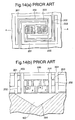
- a construction has been made such that a pair of narrow, spiral slits 201 is formed around a pixel 200 to form a cavity 204 at the bottom of the element.
- These spiral channels 202 are used as a supporting structure to support the pixel 200 afloat and wirings 203 are provided to connect to a peripheral circuit.
- the third method is to improve the ratio of an electric signal change caused by thermoelectric conversion means, dS, to a temperature change at an infrared detection portion, dTd, namely dS/dTd and is, therefore, electrical in nature.
- This method is, unlike the other two, is directed to sheer sensitization, that is, improvement of dS/dTd; however, it is quite important to reduce various electric noises generated.
- various kinds of thermoelectric conversion means have so far been investigated. Reported are, for example, a thermopile for converting a temperature change into a potential change by means of Seebeck effect (Toshio Kanno, et al., Proc. SPIE Vol. 2269, pp.
- a bolometer for converting a temperature change into a resistance change by means of the temperature change of a resistor
- a pyroelectric element for converting a temperature change into an electric charge by pyroelectric effect
- a silicon pn junction for converting a temperature change into a voltage change by certain forward currents (Tomohiro Ishikawa, et al., Proc. SPIE Vol. 3698, p. 556, 1999), etc.
- thermoelectric conversion characteristics noise characteristics and manufacturing methods.
- the bolometer is superior in terms of temperature resolution while the silicon pn junction, which can be manufactured by the silicon LSI processing alone, is superior in terms of manufacturing method.
- one of the methods for sensitizing an uncooled infrared sensor is a secondly mentioned thermal one, which improves the ratio of a temperature change at an infrared detection portion, dTd, to an incident infrared power, dP, namely dTd/dP.
- transportation of heat from an infrared detection portion to a supporting substrate is predominantly accomplished by heat conduction through a supporting structure which supports the infrared detection portion in a cavity within the supporting substrate.
- a supporting beam line to be formed within a supporting structure must be provided with a unique wiring layer made of a low thermal conductivity material.
- a supporting beam line structure using titanium material is known to be effective.
- thermoelectric conversion material in addition to the wiring process at an element peripheral circuit, another process will be required for forming a supporting beam line structure alone.
- the present invention is directed to improve the above supporting structure and to provide a highly sensitized infrared sensor and a manufacturing method thereof.
- an infrared sensor device comprising:
- an infrared sensor device comprising:
- an infrared sensor device comprising:
- the U-shaped electric conductor may have a shape of a square having one side thereof open, a circle or oval having a segment thereof open or a parabola.
- the beam line with U-shaped cross section may be rigid and elaborate, thereby considerably reducing the cross section of the supporting beam line.
- an infrared sensor comprising:
- the length of the supporting beam line may considerably be lessened and the aperture ratio, defined as an infrared detection pixel area relative to a unit pixel area, may considerably be improved.
- lessening the length of the supporting beam line may increase the mechanical strength and stabilize the operation while enabling sensitization to an infrared ray.
- linearization of the supporting beam line may extremely stabilize the manufacturing method thereof and, in turn, improvement of the yield may lower the cost.
- the chip area may be reduced by miniaturizing the peripheral circuit and, therefore, the cost may naturally be lowered.
- an inexpensive and highly sensitive uncooled infrared sensor may be obtained.
- Figs 1 through 4 represent an infrared sensor according to a first embodiment of the present invention.
- a semiconductor substrate 11 is composed of a single crystalline silicon semiconductor supporting substrate 12, an embedded silicon oxide insulating layer 13 provided on the substrate 12 and a single crystalline silicon semiconductor layer (SOI) layer 14.
- SOI silicon-on-insulator
- Partitioned on the substrate 11 is an infrared detection region 15, within which multiple holes 16 and cavities 160 are arranged in a lattice.
- Each cavity 160 is reversed pyramid in shape and the hole 16 is open on the side of the SOI layer 14 of the substrate 11, thus penetrating the SOI layer 14 and the insulating layer 13 down to the semiconductor supporting substrate 12 and having its bottom surface the supporting substrate.
- Infrared detection pixels 20 are disposed within the cavity 160 to be arranged into a matrix of two rows by two columns on the infrared detection region 15. In this embodiment, description will be made with regard to four pixels for the purpose of illustration; however, as many pixels as needed according to the desired resolution may practically be disposed in order to sense an infrared image.
- a constant current source 30, a vertical addressing circuit 40, a horizontal addressing circuit 50 and a column sample and hold circuit 60 are integrated to form a semiconductor peripheral circuit.
- Each infrared detection pixel 20 comprises a thermoelectric conversion portion 21 in which multiple, two in the drawings, pn junctions 22 are connected in series in the SOI layer 14 and an infrared absorption layer 23, laminated on the substrate, composed of a silicon oxide layer 24 and a silicon nitride layer 25. Sandwiched between the thermoelectric conversion portion 21 and the infrared absorption layer 23 is a wiring portion 26, which is laid on a wiring insulating layer 27 to contact with the n and p regions of the SOI layer 14 to form a wiring circuit.
- the infrared detection pixel 20 is suspended afloat in the hole 16 and the cavity 160 by a supporting beam line 80 and the sidewall 28 of the infrared detection pixel 20 is isolated by a gap from the surface 18 of the substrate forming the hole.
- the peripheral circuit is formed on the SOI layer 14 of the semiconductor substrate 11 and at least some transistors and capacitors comprising the circuit are of MOS type.
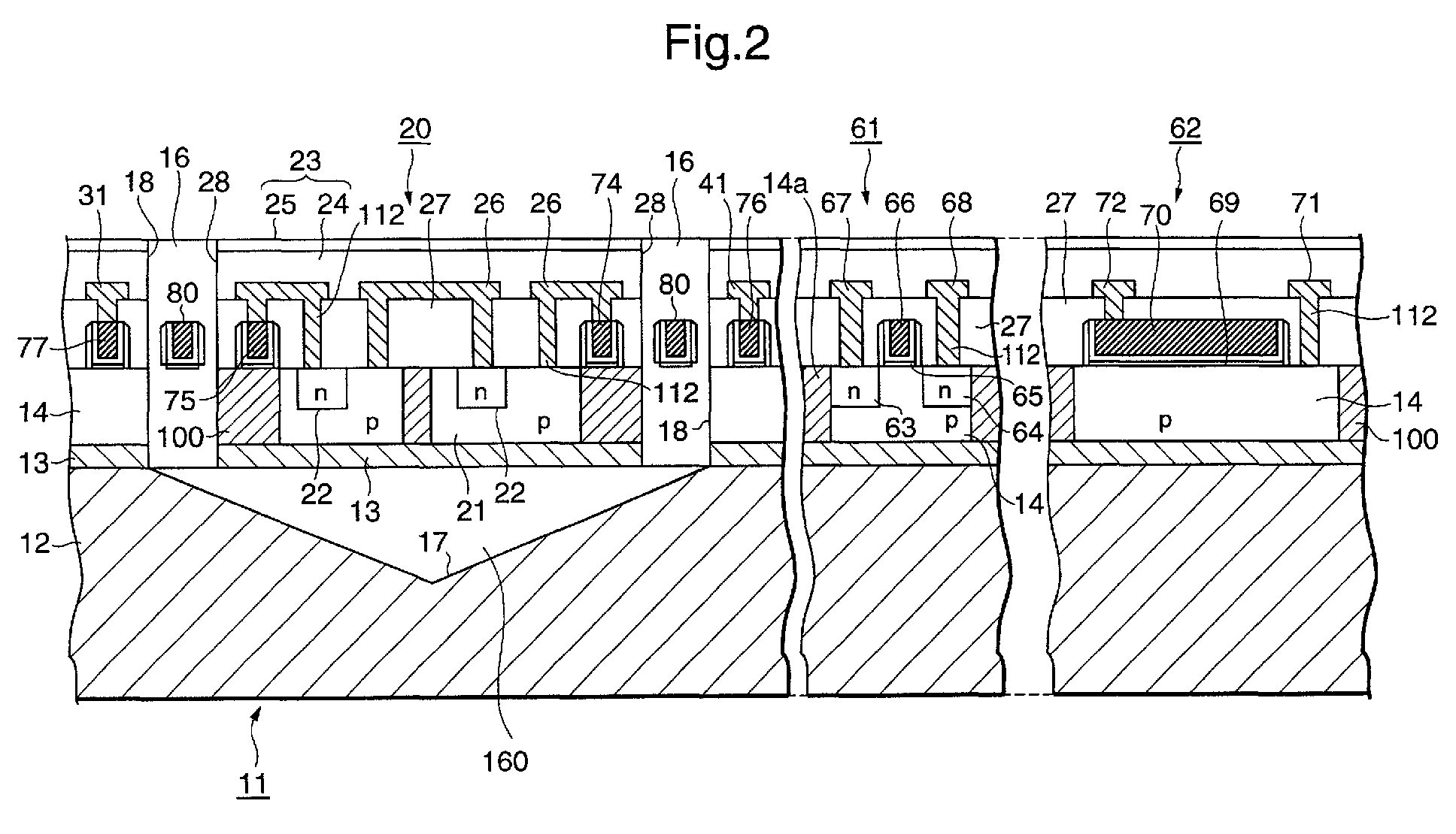
- Fig. 2 further shows a sampling MOS type transistor 61 of the column sample and hold circuit 60 and a MOS capacitor 62.
- the MOS transistor 61 forms n-type source and drain regions 63 and 64 on the p-type SOI layer 14 and also forms a channel region under the gate insulating film 65 formed on the surface 14a of the SOI layer 14.
- the gate is constructed so that it comprises a conducting layer with U-shaped cross section in the direction from the source to the drain (channel direction), inside which a metal core is filled.
- This gate electrode 66 is typically called a damascene metal gate.
- the surface of the SOI layer 14 is coated with a wiring insulating layer 27 of silicon oxide and electrodes 67 and 68 are disposed via a plug 112 of the contact hole.
- the MOS capacitor 62 is made by forming a silicon oxide insulating layer 69 on the p-type SOI layer 14 according to the same procedure as the gate insulation film 65 and sandwiching the layer 69 with the same conducting layer 70 as the damascene metal gate of the MOS transistor 61. Electrodes 71 and 72 are lead out from the p-type layer 14 and the conducting layer 70 via the plug 112 to be connected to the circuit wiring.
- the damascene metal gate electrode 66 of the MOS transistor 61, the supporting beam line 80 and the MOS capacitor 62 can be fabricated on the surface of the SOI layer 14 according to the same damascene metal process and, therefore, disposed on the same layer.
- the supporting beam line 80 comprises a conductor line with U-shaped cross section 81 and a metal 82 filled within the line.
- the conductor line 81 is in turn formed by a silicon nitride insulating layer 85 on either side and a silicon oxide insulating layer 86 at the bottom, together forming an outer insulating layer 83.
- the U-shaped conducting layer 81 is formed of an electric conductor such as titanium nitride.
- This construction is the same as the damascene metal gate construction of the MOS transistor, the U-shaped conductor line 81, the metal-filled core 82, the insulating layer 85 on either side and the insulating layer 86 at the bottom corresponding to the barrier metal, the damascene metal, the sidesurface and the gate insulating film, respectively.
- such a supporting beam line comes in a pair, one end of each of them being respectively electrically connected to a contact 74 and 75 of the wiring portion 26 of the infrared detection pixel 20 and the other end of each of them being respectively electrically connected to a contact 76 and 77 of the wirings 31 and 41 of the peripheral circuit.
- a row of the infrared detection pixel selected by the vertical addressing circuit 40 is applied with a forward bias current supplied by the constant current source 30 along the current path of the vertical signal line 31, the selected pixel 20 and the horizontal addressing line 41 and the signal voltage generated on the vertical signal line 31 is sampled and held by the column sample and hold circuit 60 and sequentially selected by the horizontal addressing circuit 50 for output.
- Fig. 1 illustrates, as a simplest embodiment, an arrangement in which the signal voltage generated on the vertical signal line 31 is directly output via the column selecting transistor (composed of a damascene metal gate MOS transistor) 51 as sequentially selected by the horizontal addressing circuit 50. Since, however, this signal voltage is so weak that by providing an arrangement in which the signal voltage is read in parallel on row by row basis, sampled by the MOS transistor 61 at the previous stage and held for one horizontal period by means of the capacitor 62, the signal voltage can be read out while reducing noises by limiting the signal bandwidth.
- a silicon nitride layer 25 and then a silicon oxide layer 24 are formed from the surface.
- infrared rays of 8 to 14 ⁇ m are absorbed and converted into heat by laminating these two absorbent materials.
- Fig. 5(a) represents infrared absorption characteristics of a silicon nitride film (CVD)
- Fig. 5(b) represents infrared absorption characteristics of a CVD deposited silicon oxide film
- Fig. 5(c) represents absorption characteristics of a heat-oxidized silicon oxide film, each at around 10 ⁇ m.
- the silicon nitride film 25 on the surface side has an absorption peak of Si-N bond at around 12 ⁇ m and the silicon oxide film 24 on the substrate side exhibits an absorption peak of Si-O bond at around 10 ⁇ m.
- the wiring portion 26 in the infrared detection pixel 20 in Fig. 3 is made of a metal such as aluminum and reflects incident infrared rays, it has an effect of increasing the absorption efficiency of infrared rays in the infrared absorption layer 23 in which such a wiring is embedded.
- the temperature of the pixel 20 is efficiently modulated by incident infrared rays.
- the infrared detection pixel 20 is supported afloat within the hole 16 and cavity 160 by the supporting beam line 80 so that the pixel wall 28 is isolated from the surface 18 of the hole and thermally isolated from the semiconductor substrate. Therefore, the incident infrared ray is absorbed in the infrared absorption layers 24 and 25 and the heat generated is only transported by the heat conduction through the supporting beam line 80 to the substrate side so that the temperature at the detection pixel 20 will increase in strict accordance with the amount of heat converted.
- the operating point of a pn junction diode within the SOI layer 14 constant-current biased due to the temperature increase is altered and the voltage of the vertical signal line 31 shown in Fig. 1 is, in turn, altered by that alteration of the operating point and read out as a signal voltage.
- the pn junctions 22 to be connected in series are two in number in the embodiment for the ease of illustration; however, more than two of them can increase the sensitivity accordingly.
- Characteristics of this embodiment lie in the construction of the supporting beam line 80 in that it is considerably miniaturized.
- the miniature supporting beam line 80 is formed simultaneously with the formation of the gate of the damascene metal gate MOS transistor.
- the U-shaped conducting line 81, the metal-filled core 82, the silicon nitride insulating layer 85 and the bottom insulating layer 86 correspond respectively to the barrier metal, the damascene metal, the sidewall and the gate insulation film of the MOS transistor.
- MOS transistor of a damascene metal is described in detail by A. Yagishita et al. in an article "High Performance Damascene Metal Gate MOSFET's for 0.1 ⁇ m Regime," IEEE Trans. On Electron Devices, Vol. 47, No. 5, p. 1028, May 2000. Also in this embodiment, a similar procedure has been used to form a damascene metal gate and, at the same time, to implement the extremely miniature supporting beam line 80.
- Figs. 6 and 7 The steps for manufacturing a damascene metal gate MOS transistor and the steps to be carried out simultaneously therewith for manufacturing a supporting beam line made of a damascene metal wiring are shown respectively in Figs. 6 and 7, wherein like reference characters denote like steps in both figures to be carried out simultaneously.
- Fig. 6 differs from Fig. 7 with respect to that, in Fig. 6, doped regions 63 and 64 for the source and drain are formed on a p-type semiconductor layer 14 for operating as a transistor and a damascene metal gate 66 is formed on the semiconductor layer 14, since Fig. 6 illustrates the steps for manufacturing a MOS transistor. On the other hand, in Fig. 7, since it illustrates the steps for manufacturing a wiring, it is formed on shallow trench isolation (STI) region 100, an isolation region, and naturally an impurity layer does not have to be formed.
- STI shallow trench isolation
- the supporting substrate 12 (Fig. 2) has been omitted to illustrate only the embedded silicon oxide insulating layer 13 and the semiconductor layer (SOI) layer 14 thereon for describing the manufacturing steps below.
- Step (a) in Fig. 6, as a well-known LSI manufacturing step, an element isolating insulation region 100a, a gate oxide film 101 and a MOS transistor gate have been formed on an SOI layer 14. In Fig. 7, the same step corresponds to formation of a supporting beam line.
- an element isolation region (STI) region 100a of a silicon oxide insulating layer is produced by shallow trench isolation (STI) process surrounding a MOS transistor region while at Step (a) in Fig. 7, the whole region is subjected to STI process to form an STI region 100 in which silicon oxide is embedded.
- STI shallow trench isolation
- a silicon oxide dummy oxide film 101 is first formed and then, as a dummy gate, a polysilicon film 102 and a silicon nitride film 103 thereon are deposited, followed by an etching by reactive ion etching (RIE), etc. using a photoresist 104 as a mask to provide a protrusion.
- RIE reactive ion etching
- a lightly doped drain (LDD) doped region is formed by impurity ion implantation in a self-aligned manner to the dummy gate.
- a sidewall 105 is formed by a general procedure of depositing a silicon nitride film over the whole surface before etching the whole surface by RIE to leave the sidewall. Another ion implantation will form doped regions 63 and 64 for the source and drain in a self-aligned manner to the sidewall 105.
- the photoresist 104 used at Step (a) has been eliminated by ashing with oxygen, etc. before forming the sidewall 105 before or after forming the LDD doped regions.
- the step of forming a doped region is not performed, but the sidewall 105 is formed.
- insulation film deposition for the damascene metal process and flattening by chemical mechanical polishing (CMP) are performed.
- a silicon oxide film is deposited by CVD using TEOS as a source and is flattened by CMP.
- the sidewall 105 and the dummy gate 103 on the surface side have been formed by a silicon nitride film and, during the process, function as a stopper in CMP.
- the dummy gates 103 and 102 as well as the dummy oxide film 101 are sequentially removed.
- the dummy gate 103 made of silicon nitride is removed by hot phosphoric acid while the dummy gate 102 made of polysilicon and part of the dummy oxide film 101 are removed by chemical dry etching (CDE).
- CDE chemical dry etching
- small remaining portion of the dummy oxide film 101 is removed by dilute hydrofluoric acid, for example.
- the STI region 100 is slightly etched.
- a silicon oxide film or a tantalum oxide film is formed as a gate insulation film 106, and a titanium nitride film for example as a barrier metal 107 for preventing diffusion from the damascene metal 108 is deposited by a technique such as sputtering or CVD, before depositing aluminum or tungsten for example as a damascene metal 108 by a depositing technique such as sputtering or CVD and removing the dummy gates 102 and 103 to completely embed the groove formed.
- a technique such as sputtering or CVD
- Step (f) flattens and eliminates the barrier metal 107 in the region other than the damascene metal 108 and the gate by CMP to provide a MOS transistor 61 having a damascene metal gate 66 and a basic structure of a supporting beam line 80 having a similar construction as the gate.
- Steps (g) through (i) after the supporting beam line in Fig. 7 are related to the formation of the hole 16 to be described later.
- the PMD layer 111 and the STI layer 100 on both sides as well as the embedded insulating layer 13 are etched by anisotropic etching RIE using the silicon nitride sidewall 105 as a mask.
- the STI layer 100 and the embedded insulating layer 13 are etched to leave a U-shaped conductor line 81 (barrier metal 107) externally coated with the insulating layer 85 (sidewall 105) and the bottom insulating layer 86 (gate insulation film 106) as well as a metal portion 82 (damascene metal 108) filled within the U-shaped groove. This is to be the supporting beam line 80.
- the damascene metal 108 is etched away to leave structures with U-shaped cross section 81, 85 and 86, which may be obtained as a modification of the supporting beam line 80.
- the cross section of the MOS transistor 61 used in the element peripheral circuit in Fig. 2, the infrared detection pixel 20 and the supporting beam line are additionally illustrated. It will be described that the supporting beam line 80 is formed on the SOI layer 14 on the same layer with the gate electrode 66 of the MOS transistor.
- a so-called SOI substrate is provided as a semiconductor substrate 11 in which an embedded silicon oxide layer 13 and a single crystalline silicon layer (SOI layer) 14 are sequentially laminated on a single crystalline silicon substrate 12.
- a shallow trench isolation (STI) process is performed as an example of isolation in a typical LSI manufacturing process. Specifically, isolation regions are partitioned using a technique such as photolithography and the single crystalline silicon layer 14 of the isolation regions is etched away using a technique such as reactive ion etching (RIE), followed by embedding an isolation silicon oxide film 100 by a technique such as chemical vapor deposition (CVD) and flattening by a technique such as chemical mechanical polishing (CMP). During this process, the region for the supporting beam line is defined as an isolation region, in which an isolation silicon oxide film (STI layer) 100 is embedded.
- RIE reactive ion etching
- an infrared detection pixel 20 is formed according to the method described above along with the damascene metal gate transistor 61 and the supporting beam line 80 to be used for the peripheral circuit for the addressing circuits 40 and 50, the output portion 60, the constant current source 30, etc.
- the region in the SOI layer 14 where the detection pixels are partitioned is a p-type semiconductor, in which an n-type region is diffused to form multiple pn junctions 22.
- an insulating layer 27 is formed on the SOI layer and contact holes are formed by RIE for example and stuffed with plugs 112 if necessary.
- plugs 112 may be embedded by depositing a tungsten film on the whole substrate by CVD and then performing CMP.
- the gate electrode 66 and the supporting beam line 80 are to be formed with contact holes, which are stuffed with plugs 112.
- a barrier metal layer 89 (Fig. 8(c)) made of titanium, titanium nitride or a laminated film thereof for example may be formed within the contact hole.
- a metal wiring portion 26 to be connected to the plug will then be formed.
- the wiring is made of aluminum or aluminum alloy for example.
- an infrared absorption layer 23 is formed also serving for passivation of the MOS transistor, etc.
- a silicon oxide film 24 is laminated with a silicon nitride film 25.
- a capacitor 62 to be used in the peripheral circuit is formed by the same process as the damascene metal gate MOS transistor 61 and the supporting beam line 80.
- MOS capacitor having a construction in which the p-type SOI layer 14 is one of the electrodes with a barrier metal layer formed on the insulating layer 69 and the damascene metal layer 70 is the other electrode is obtained and completely electrically isolated on the SOI substrate.
- this construction has only one metal layer, it can be made thin and, consequently, the infrared detection portion may be thin when the sensor surface is flattened, enabling to reduce heat capacity of the infrared detection portion and improving the response as well as enabling to reduce image lag.
- the hole 16 is etched by RIE so that the hole has an opening on the side of the SOI layer 14. The etching is performed through the SOI layer 14 and the embedded insulating layer 13 until the single crystalline silicon supporting substrate 12 is exposed.
- Fig. 14 shown as a conventional example, the formation of an etched hole 201 is limited in its miniaturization by the limit of lithography, etc. According to the construction of this embodiment, however, a considerable degree of miniaturization is possible, so that the etched hole 16 may be designed to accommodate the supporting beam line 80.
- a hole for retaining a pixel afloat is formed for each pixel, the hole having an opening of more or less large in size in accordance with the squareness of the pixel.
- the four sides of the pixel are applied with a photoresist mask having a frame-like opening.
- the supporting beam line 80 is disposed so that it is located just below the opening of the mask.
- Such a construction is possible because the etching resistance of the silicon nitride of the sidewall is high against the etchant for silicon etching of the supporting substrate 12.
- silicon anisotropic etching is carried out for forming a cavity 160.
- a liquid agent such as tetramethyl ammonium hydroxide (TMAH) as an anisotropic etchant for single crystalline silicon to carry out an anisotropic etching of single crystalline silicon scoops out the bottom of the pixel to form the cavity 160 within the single crystalline silicon supporting substrate 12 so that the block-like pixel 20 may be suspended by the supporting beam line 80.
- TMAH tetramethyl ammonium hydroxide
- Step (h) in Fig. 7 the silicon oxide is etched using an etchant for silicon oxide having a high selectivity with aluminum to eliminate the remaining STI region 100 below the supporting beam line 80.
- the width of the supporting beam line 80 is considerably reduced since it can be constructed together with the damascene metal gate of the MOS transistor.
- the width of the supporting beam line will be 0.23 micron, which can easily be obtained by etching, to provide a linear supporting beam line structure as shown in Fig. 4.
- a liquid mixture of acetic acid and ammonium fluoride having a high selectivity with aluminum may preferably be used.
- the supporting beam line 80 is designed in a double spiral fashion as in a third embodiment (Fig. 9) for super-high sensitization, it is possible to leave the STI region 100 below the supporting beam line 80 not completely etched. Even in that case, the thermal conductivity of the silicon oxide film which is a material for the STI region is 15 [W/m/K] or so and, considering the relationship with the mechanical strength for supporting the infrared detection portion 20, the design may be optional and optimal depending on its purposes.
- the cross sectional area of the supporting beam line is considerably reduced and a considerable degree of sensitization may be possible due to a considerable reduction of heat conduction.
- it is not only possible to decrease the width of the supporting beam line over the limit of miniaturization made possible by lithography processing, but as well to virtually decrease the heat conduction down to the level predominated only by the supporting beam line.
- formation on the same layer as the gate electrode of the MOS transistor enables an extremely fine processing, consequently reducing the heat conduction and allowing for sensitization.
- the thermal conductivity for a typical supporting beam line as shown in Fig. 14 is 1 ⁇ 10 -7 [W/K], which implies that the length of the supporting beam line according to this embodiment would be as short as 3.2 micron.
- a linear supporting beam line 80 is feasible and, consequently, a fill factor, the area of an infrared detection portion 20 occupied by a pixel, may considerably be improved.
- the whole chip area may be reduced and, as a result, reduction of the expense may be effected.
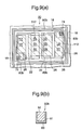
- Fig. 8 (a), (b)and (c) illustrate an infrared detection pixel portion according to a second embodiment of the present invention, wherein like reference characters denote like parts as in the first embodiment.
- Fig. 8(b) illustrating an enlarged cross section of a supporting beam line 80a in relation to the first embodiment shown in Fig. 2, the construction is of Step (i) in Fig. 7, a construction of a supporting beam line 80 from which a damascene metal 108 has been eliminated.
- the thermal conductivity per unit length of the supporting beam line 80a is further reduced to enable sensitization and simplification of the construction.
- the manufacturing method thereof is substantially the same as the first embodiment, basically with the exception of the added process of eliminating the damascene metal 108.
- the damascene metal 108 when aluminum is used as the damascene metal 108, the damascene metal will be etched by a silicon etchant, TMAH, in the process of forming the hole 16 by etching the supporting substrate 6 as shown in Step (i) in Fig. 7, with no additional process required.
- TMAH silicon etchant
- the thermal conductivity per unit length of the supporting beam line according to this embodiment would considerably be reduced down to 1.6 ⁇ 10 -13 [W/m/K].
- the length of the supporting beam line is even less than that of the first embodiment, allowing to further reduce the heat conduction from the wall of the detection pixel to the surface of the hole.
- the supporting beam line has no damascene metal so that the U-shaped conductor line may serve as a current path.
- the bottom of the supporting beam line 11 may be left with some STI region.
- the design may be optional and optimal depending on its purposes.
- a pair of supporting beam lines 80b is connected respectively to the vertical signal line and to the horizontal signal line.
- Each of these supporting beam lines extends in a double spiral fashion along two sides of the square infrared detection pixel 20 to be connected to the wiring contact portion on the side to the surface 18 of the hole.
- the supporting beam line 80b is not provided with an outer insulating layer (sidewall) and comprises a U-shaped conductor line 81, a bottom insulating layer 86 and a filled metal 82.
- the supporting beam line 80b having such a spiral pattern can lengthen the heat conduction path and is, therefore, suitable for a sensitive sensor.
- the metal 82 filled in the U-shaped conductor line contributes to the mechanical strength and the reduction of electric resistance and is suitable for a structure having a spiral pattern.
- a supporting beam line 80c comprises a U-shaped conductor layer 84 and a bottom insulating layer 86 disposed at the bottom thereof and extends linearly. No filled metal is provided.
- the third and fourth embodiments have substantially the same construction as the first and second embodiments, but are characterized in that they have no outer insulating layers (sidewalls) 85 on the supporting beam lines 80b and 80c.
- a manufacturing method for obtaining this construction may be carried out only by adjusting the etching conditions for forming the hole 16 respectively in the first and second embodiments, with virtually no additional processes needed.
- etching conditions in which the selectivity between the silicon oxide film and the silicon nitride film is low can be used to etch the outer insulating layer of the silicon nitride to obtain the constructions in Figs. 9 and 10.
- the third embodiment would produce substantially the same results as in the first embodiment, whereas the thermal conductivity per unit length of the supporting beam line in the fourth embodiment would appreciably decrease down to 7.3 ⁇ 10 -14 [W/m/K].
- a length of 1.5 micron would be enough for a supporting beam line according to this embodiment, enabling a reduction of the length down to about 1/50 of the length of the structure in Fig. 14.
- the supporting beam line 80c serving also as a supporting leg as shown in the fourth embodiment can be implemented linearly, thereby considerably improving a fill factor, the ratio of the area of the infrared detection portion 20 occupied by the pixel.
- the aforementioned effect of optical sensitization may thereby be obtained as well.
- the supporting beam line according to the fourth embodiment has a linear pattern, its mechanical strength and stability will considerably be improved as well analogously to the first and second embodiments.
- a supporting beam line 80d has the same construction as in the first embodiment as shown in Fig. 11(b).
- Each process for implementing the construction according to the fifth embodiment is basically the same as each of those in the first embodiment. The only difference is the elimination of the embedded oxide film layer 13, which is enabled by increasing the period of time for etching the silicon oxide of the STI region 100 at the bottom of the supporting beam line 80d (Step (g) in Fig. 7) after etching the supporting substrate 11.
- the heat transportation by emission from the back face 19 of the pixel 20 is suppressed so that the limit of sensitization associated with the miniaturization of the supporting beam line may be shifted upward.
- the bottom of the infrared detection pixel is provided with a silicon oxide film 13 which is an embedded insulating layer.
- the silicon oxide film exhibits an absorption at 10 ⁇ m band arising from the presence of an Si-O bond, as shown in Fig. 5(b) and 5(c). It particularly means that the emissivity at 10 ⁇ m band is high, suggesting that the temperature of the pixel 20 raised by an incident infrared ray will be lowered by the heat transportation through the emission from the silicon oxide film at the bottom.
- the heat conductance of the supporting structure Due to the miniaturization of the supporting structure, the heat conductance of the supporting structure has been realized at a value of 10 -7 [W/m/K] or so. However, according to the present invention, when the heat conductance becomes 10 -8 [W/m/K] or so, the heat transportation by the emission from the back face described above will predominate, bringing about the limit of sensitization.
- the most of the back face of the sensor portion 19 has the exposed SOI layer 14 of single crystalline silicon. Since single crystalline silicon contains very little impurity, it does not exhibit a peak of infrared absorption arising from the Si-O bond and, therefore, has an extremely low emissivity.
- the limit of sensitization in a trend of miniaturizing a supporting beam line can further be raised.
- the supporting beam line may have the construction according to any of Figs. 8 through 10.
- each of the embodiments having so far been described relates to an infrared sensor device comprising multiple infrared detection elements arranged in a matrix in a two-dimensional manner, it may also be applied to a one-dimensional sensor comprising infrared detection elements arranged in a one-dimension manner or a single infrared sensor not arranged in any array or matrix, with the similar effects obtained.
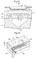
- an infrared absorption layer 23a is formed on an infrared detection pixel 20 as an umbrella-shaped body having an area larger than the pixel.
- This umbrella-like absorption layer 122 is laminated with a reflective layer 120 as a ground and an insulating layer 121 as an intermediate, for example. In this manner, providing a larger area will improve the fill factor of the pixel 20.
- the supporting beam line 80e according to each of the embodiments of the present invention is applicable to an infrared detection pixel which is used for a thermoelectric conversion portion as shown in Fig. 13 in which pn junctions 22a of a lateral construction are connected in series by wirings 26a.
- thermoelectric conversion means is not limited to an infrared detection portion which employs pn junctions for thermoelectric conversion means and, on the contrary, may be used for an infrared detection portion which uses a bolometer, etc. as thermoelectric conversion means to provide for fine processability as well as sensitization and cost reduction due to the effect of shortening the processing.
Landscapes
- Physics & Mathematics (AREA)
- General Physics & Mathematics (AREA)
- Spectroscopy & Molecular Physics (AREA)
- Solid State Image Pick-Up Elements (AREA)
- Photometry And Measurement Of Optical Pulse Characteristics (AREA)
- Radiation Pyrometers (AREA)
- Electrodes Of Semiconductors (AREA)
- Thin Film Transistor (AREA)
Abstract
Description
Claims (18)
- An infrared sensor device comprising:a semiconductor substrate having a principal plane including a surface portion in which a hole is provided;an infrared detection pixel disposed in the hole, comprising an infrared absorption portion configured to absorb an infrared ray and convert it into heat and a thermoelectric conversion portion configured to convert the heat into an electric signal;a semiconductor peripheral circuit, disposed on the principal plane of the substrate, configured to read out the electric signal from the infrared detection pixel; anda supporting beam line with U-shaped cross section, extending across the infrared detection pixel and the surface portion having the hole, configured to support the infrared detection pixel, afloat within the hole and to electrically connect the infrared detection pixel to the semiconductor peripheral circuit.
- An infrared sensor device according to Claim 1, wherein the supporting beam line comprises an electric conductor.
- An infrared sensor device according to Claim 2, wherein the electric conductor is made of titanium nitride.
- An infrared sensor device according to either of claims 2 or 3, wherein the supporting beam line further comprises an insulating layer.
- An infrared sensor device according to Claim 4, wherein the insulating layer is made of silicon nitride.
- An infrared sensor device according to Claim 1, wherein a metal member is inserted inside the supporting beam line.
- An infrared sensor device comprising:a semiconductor substrate having a principal plane including a plurality of surface portions in each of which a hole is provided;
a plurality of infrared detection pixels each disposed in the hole, each comprising an infrared absorption portion, configured to absorb an infrared ray and to convert it into heat and a thermoelectric conversion portion configured to convert the heat into an electric signal;
a semiconductor peripheral circuit, disposed on the principal plane of the substrate, configured to read out the electric signals from the infrared detection pixels, the semiconductor peripheral circuit including at least a MOS transistor having a gate comprising a first electric conductor with U-shaped cross section along the directions of the source and drain and a metal filled within the electric conductor; and
a plurality of supporting beam lines, each extending across the infrared detection pixel and the surface portion having the hole, configured to support the infrared detection pixel, afloat within the hole and configured to electrically connect the infrared detection pixels to the semiconductor peripheral circuit, each of the supporting beam lines including at least a second electric conductor with U-shaped cross section and being formed in the same layer as the first electric conductor with U-shaped cross section of the gate of the MOS transistor. - An infrared sensor device comprising:a semiconductor substrate having a semiconductor supporting substrate and a semiconductor layer and an insulating layer interposed therebetween, in which a plurality of holes are provided on the semiconductor substrate, the holes penetrating the semiconductor layer and the insulating layer to reach the semiconductor supporting substrate;a plurality of infrared detection pixels each disposed in each of the holes, each comprising an infrared absorption portion configured to absorb an infrared ray and to convert it into heat and a thermoelectric conversion portion configured to convert the heat into an electric signal;a semiconductor peripheral circuit, formed on the semiconductor layer, including at least a MOS transistor having a damascene metal gate formed for driving the infrared detection pixels to read out the electric signal; anddamascene metal supporting beam lines, extending across the infrared detection pixels and side surfaces of the holes of the semiconductor substrate respectively, configured to support the infrared detection pixel, afloat within the holes respectively and to electrically connect the infrared detection pixels to the semiconductor peripheral circuit respectively, the damascene metal supporting beam lines being disposed in the same layer as the damascene metal gate.
- An infrared sensor device comprising:a semiconductor substrate having a semiconductor supporting substrate and a semiconductor layer and an insulating layer interposed therebetween, in which a plurality of holes are provided on the semiconductor substrate, the holes penetrating the semiconductor layer and the insulating layer to reach the semiconductor supporting substrate;
layer to reach the semiconductor supporting substrate;a plurality of infrared detection pixels each disposed in each of the holes, each comprising an infrared absorption portion configured to absorb an infrared ray and to convert it into heat and a thermoelectric conversion portion configured to convert the heat into an electric signal, the plurality of infrared detection pixels being arranged in a matrix and connected by horizontal and vertical wirings;a semiconductor peripheral circuit comprising a pixel selecting circuit, formed on the semiconductor layer and connected to the horizontal wiring, configured to select the infrared detection pixel from which the signal is to be read, a pixel signal reading circuit, connected to the vertical wiring, configured to read out the signal from the infrared detection pixel selected by the pixel selecting circuit and an outputting circuit configured to output the signal read out by the reading circuit and also including a MOS transistor having a damascene metal gate; anda damascene metal supporting beam lines, extending across the infrared detection pixels and side surfaces of the hales of the semiconductor substrate respectively configured to support the infrared detection pixel afloat within the holes respectively and to connect the infrared detection pixels to the horizontal and vertical wirings, the damascene metal supporting beam line being disposed in the same layer as the damascene metal gate. - An infrared sensor device according to Claim 9, wherein each of the supporting beam lines is disposed below the horizontal and vertical wirings.
- An infrared sensor device according to any preceding claim, wherein the supporting beam line is linear.
- An infrared sensor device according to any preceding claim, wherein the thermoelectric conversion portion of the infrared detection pixel has a pn junction.
- An infrared sensor device according to any preceding claim, wherein the infrared absorption portion comprises a silicon oxide film and a silicon nitride film laminated thereon.
- An infrared sensor device according to Claim 8, wherein the semiconductor peripheral circuit includes a MOS capacitor formed on the semiconductor layer, an electrode of the MOS capacitor being disposed in the same layer as the damascene metal gate of the MOS transistor.
- An infrared sensor device according to any preceding claim, wherein the semiconductor substrate and the thermoelectric conversion portion of the infrared detection pixel are made of single crystalline silicon and the bottom surface of the hole of the semiconductor substrate is directly opposed to the bottom surface of the thermoelectric conversion portion.
- A method of manufacturing an infrared sensor, comprising:embedding a silicon oxide layer in a substrate comprising a single crystalline silicon supporting substrate, an silicon oxide film layer formed on the single crystalline silicon supporting substrate and a single crystalline silicon layer formed on the silicon oxide film layer, over a predetermined region of the single crystalline silicon layer;forming a thermoelectric converter pn junction for an infrared detection pixel in the single crystalline silicon layer;forming a supporting beam line including a U-shaped electric conductor on the silicon oxide layer while forming a gate electrode of a MOS transistor having an electric conductor with U-shaped cross section, the MOS transistor being included in a peripheral circuit on the single crystalline silicon layer;forming an infrared absorption layer on the single crystalline silicon layer; andforming a hole by etching for isolating the infrared detection pixel of the substrate from the substrate and suspending the infrared detection pixel within the hole by the supporting beam line.
- A method of manufacturing an infrared sensor, comprising:forming an isolation recess region on an SOI substrate comprising at least a single crystalline silicon supporting substrate, a silicon oxide layer formed on the single crystalline silicon supporting substrate and a single crystalline silicon layer formed on the silicon oxide layer by etching the single crystalline silicon layer;embedding an isolating silicon oxide film in the isolation recess region;forming a supporting beam line layer having a U shape simultaneously with the gate electrode of a damascene metal gate MOS transistor being formed on an element peripheral circuit;forming a thermoelectric conversion portion in the single crystalline silicon layer;forming a wiring for outputting an electric signal from the thermoelectric conversion portion;forming an infrared absorption layer on the single crystalline silicon layer; andforming a hole surrounding the thermoelectric conversion portion by etching for penetrating the single crystalline silicon layer and the silicon oxide layer of the SOI substrate to isolate the thermoelectric conversion portion from the SOI substrate to make an infrared detection pixel while forming a supporting beam line supporting the infrared detection pixel.
- A method of manufacturing an infrared sensor device, comprising the steps of:partitioning, on a single crystalline silicon substrate, locations for an infrared detection pixel, a peripheral circuit for reading out a signal from the detection pixel and a supporting beam line around the detection pixel for suspending the detection pixel and embedding a silicon oxide insulating layer at least at the location for the supporting beam line;forming a silicon protrusion on the insulating layer and forming a silicon nitride insulating layer on the sidewall thereof;eliminating the silicon protrusion and forming a conducting layer inside the silicon nitride insulating layer;depositing an infrared absorption layer on the detection pixel; andetching the periphery of the detection pixel, leaving the silicon nitride insulating layer and the conducting layer, to form a hole for disposing the detection pixel afloat from the substrate by using the insulating layer and the conductive layer as the supporting beam line.
Priority Applications (1)
| Application Number | Priority Date | Filing Date | Title |
|---|---|---|---|
| EP05008367A EP1553633A3 (en) | 2001-03-30 | 2002-03-28 | Infrared sensor device and manufacturing method thereof |
Applications Claiming Priority (2)
| Application Number | Priority Date | Filing Date | Title |
|---|---|---|---|
| JP2001100402A JP3589997B2 (en) | 2001-03-30 | 2001-03-30 | Infrared sensor and method of manufacturing the same |
| JP2001100402 | 2001-03-30 |
Related Child Applications (1)
| Application Number | Title | Priority Date | Filing Date |
|---|---|---|---|
| EP05008367A Division EP1553633A3 (en) | 2001-03-30 | 2002-03-28 | Infrared sensor device and manufacturing method thereof |
Publications (2)
| Publication Number | Publication Date |
|---|---|
| EP1246251A2 true EP1246251A2 (en) | 2002-10-02 |
| EP1246251A3 EP1246251A3 (en) | 2004-03-03 |
Family
ID=18953845
Family Applications (2)
| Application Number | Title | Priority Date | Filing Date |
|---|---|---|---|
| EP05008367A Withdrawn EP1553633A3 (en) | 2001-03-30 | 2002-03-28 | Infrared sensor device and manufacturing method thereof |
| EP02252282A Withdrawn EP1246251A3 (en) | 2001-03-30 | 2002-03-28 | Infrared sensor device and manufacturing method thereof |
Family Applications Before (1)
| Application Number | Title | Priority Date | Filing Date |
|---|---|---|---|
| EP05008367A Withdrawn EP1553633A3 (en) | 2001-03-30 | 2002-03-28 | Infrared sensor device and manufacturing method thereof |
Country Status (4)
| Country | Link |
|---|---|
| US (3) | US6806470B2 (en) |
| EP (2) | EP1553633A3 (en) |
| JP (1) | JP3589997B2 (en) |
| KR (1) | KR100547064B1 (en) |
Cited By (5)
| Publication number | Priority date | Publication date | Assignee | Title |
|---|---|---|---|---|
| US8080795B2 (en) | 2007-08-02 | 2011-12-20 | Technische Universitaet Muenchen | Device for imaging and method for producing the device |
| FR2980915A1 (en) * | 2011-09-30 | 2013-04-05 | St Microelectronics Crolles 2 | Method for manufacturing e.g. metal-oxide semiconductor transistors in zones of semiconductor substrate of complementary metal-oxide semiconductor integrated circuit, involves filling openings with conducting material |
| WO2013171020A1 (en) * | 2012-05-16 | 2013-11-21 | Robert Bosch Gmbh | Infrared sensor device and method for producing an infrared sensor device |
| RU2515214C2 (en) * | 2009-08-11 | 2014-05-10 | Айвьютек Ко., Лтд | Electronic device |
| CN110767667A (en) * | 2019-11-26 | 2020-02-07 | 上海微阱电子科技有限公司 | An image sensor structure and forming method |
Families Citing this family (54)
| Publication number | Priority date | Publication date | Assignee | Title |
|---|---|---|---|---|
| US6888219B2 (en) * | 2002-08-29 | 2005-05-03 | Honeywell International, Inc. | Integrated structure with microwave components |
| WO2004068574A1 (en) * | 2003-01-30 | 2004-08-12 | X-Fab Semiconductor Foundries Ag | Soi contact structure(s) and corresponding production method |
| KR100538996B1 (en) * | 2003-06-19 | 2005-12-27 | 한국전자통신연구원 | Infrared ray sensor using silicon oxide film as a infrared ray absorption layer and method for fabricating the same |
| US7170059B2 (en) * | 2003-10-03 | 2007-01-30 | Wood Roland A | Planar thermal array |
| KR100539395B1 (en) * | 2003-10-09 | 2005-12-27 | 이홍기 | Uncooled infrared sensor with two-layer structure |
| US7154136B2 (en) * | 2004-02-20 | 2006-12-26 | Micron Technology, Inc. | Isolation structures for preventing photons and carriers from reaching active areas and methods of formation |
| US7492027B2 (en) * | 2004-02-20 | 2009-02-17 | Micron Technology, Inc. | Reduced crosstalk sensor and method of formation |
| US8716814B2 (en) * | 2004-07-14 | 2014-05-06 | Semiconductor Energy Laboratory Co., Ltd. | Wireless processor, wireless memory, information system, and semiconductor device |
| CN100479171C (en) * | 2004-07-14 | 2009-04-15 | 株式会社半导体能源研究所 | Wireless processor, wireless memory, information system, and semiconductor device |
| US7442933B2 (en) | 2005-02-03 | 2008-10-28 | Lin Alice L | Bolometer having an amorphous titanium oxide layer with high resistance stability |
| WO2006103104A1 (en) * | 2005-04-01 | 2006-10-05 | Trumpf Werkzeugmaschinen Gmbh + Co. Kg | Optical element and method for recording beam parameters, comprising a temperature sensor provided in the form of a pixel matrix |
| US7858481B2 (en) | 2005-06-15 | 2010-12-28 | Intel Corporation | Method for fabricating transistor with thinned channel |
| US7332756B2 (en) * | 2005-11-21 | 2008-02-19 | Taiwan Semiconductor Manufacturing Co., Ltd. | Damascene gate structure with a resistive device |
| JP4528720B2 (en) * | 2005-12-28 | 2010-08-18 | 株式会社東芝 | Infrared detecting element, manufacturing method thereof and infrared camera |
| JP2009538425A (en) * | 2006-05-23 | 2009-11-05 | リージェンツ オブ ザ ユニバーシティ オブ ミネソタ | Thermal detector and infrared sensing method |
| JP2008028240A (en) * | 2006-07-24 | 2008-02-07 | Toshiba Corp | Solid-state imaging device |
| KR100809933B1 (en) * | 2006-10-21 | 2008-03-06 | (주)한비젼 | Semiconductor device and manufacturing method thereof |
| JP2010512507A (en) * | 2006-12-08 | 2010-04-22 | リージェンツ オブ ザ ユニバーシティ オブ ミネソタ | Detection beyond standard radiated noise limits using emissivity reduction and optical cavity coupling |
| US7851861B2 (en) * | 2007-01-22 | 2010-12-14 | Taiwan Semiconductor Manufacturing Co., Ltd. | MIM capacitor and metal gate transistor |
| US20090014657A1 (en) * | 2007-05-01 | 2009-01-15 | Honeywell International Inc. | Infrared fire detection system |
| US7746236B2 (en) * | 2007-05-01 | 2010-06-29 | Honeywell International Inc. | Fire detection system and method |
| US7622717B2 (en) * | 2007-08-22 | 2009-11-24 | Drs Sensors & Targeting Systems, Inc. | Pixel structure having an umbrella type absorber with one or more recesses or channels sized to increase radiation absorption |
| US12546666B2 (en) | 2007-08-29 | 2026-02-10 | Texas Instruments Incorporated | Apparatus and method to test embedded thermoelectric devices |
| US11133350B2 (en) * | 2007-08-29 | 2021-09-28 | Texas Instruments Incorporated | Integrated circuit with thermoelectric power supply |
| JP5357430B2 (en) * | 2008-02-04 | 2013-12-04 | 株式会社ユニバーサルエンターテインメント | Infrared sensor |
| US7888763B2 (en) * | 2008-02-08 | 2011-02-15 | Omnivision Technologies, Inc. | Backside illuminated imaging sensor with improved infrared sensitivity |
| JP5108566B2 (en) * | 2008-03-11 | 2012-12-26 | ラピスセミコンダクタ株式会社 | Infrared detector manufacturing method |
| WO2010033142A1 (en) | 2008-05-30 | 2010-03-25 | Regents Of The University Of Minnesota | Detection beyond the standard radiation noise limit using spectrally selective absorption |
| JP2010078449A (en) * | 2008-09-25 | 2010-04-08 | Toshiba Corp | Infrared imaging element and method for manufacturing the same |
| JP5543703B2 (en) * | 2008-09-25 | 2014-07-09 | 株式会社東芝 | Subject position detection element |
| US8658935B2 (en) * | 2008-12-24 | 2014-02-25 | Chemetron-Railway Products, Inc. | Welding process with jerk compensation |
| US8604435B2 (en) * | 2009-02-26 | 2013-12-10 | Texas Instruments Incorporated | Infrared sensor structure and method |
| KR20110019238A (en) * | 2009-08-19 | 2011-02-25 | 삼성전자주식회사 | Touch panel |
| WO2011030413A1 (en) * | 2009-09-09 | 2011-03-17 | 株式会社 東芝 | Solid-state image pickup device and method for manufacturing same |
| KR101648353B1 (en) * | 2009-09-25 | 2016-08-17 | 삼성전자 주식회사 | Image sensor having depth sensor |
| JP5687202B2 (en) * | 2009-11-04 | 2015-03-18 | ローム株式会社 | Pressure sensor and pressure sensor manufacturing method |
| JP5143176B2 (en) * | 2010-03-31 | 2013-02-13 | 株式会社東芝 | Infrared imaging device and manufacturing method thereof |
| US8941064B2 (en) | 2010-04-12 | 2015-01-27 | Mikrosens Elektronik San. Ve Tic. A.S. | Uncooled infrared detector and methods for manufacturing the same |
| US8411442B2 (en) * | 2010-09-09 | 2013-04-02 | Texas Instruments Incorporated | Vias in substrate between IC seat and peripheral thermal cage |
| US8557624B2 (en) * | 2011-01-13 | 2013-10-15 | International Business Machines Corporation | Pixel sensor cells with a split-dielectric transfer gate |
| JP5731862B2 (en) * | 2011-03-11 | 2015-06-10 | 株式会社東芝 | Uncooled infrared imaging device and manufacturing method thereof |
| TWI439679B (en) * | 2011-08-03 | 2014-06-01 | Univ Nat Chiao Tung | Electric school radiometer |
| JP5738225B2 (en) * | 2012-03-22 | 2015-06-17 | 三菱電機株式会社 | Thermal infrared solid-state imaging device and manufacturing method thereof |
| DE102012218414A1 (en) * | 2012-10-10 | 2014-04-10 | Robert Bosch Gmbh | Integrated diode arrangement and corresponding manufacturing method |
| JP2016033973A (en) * | 2014-07-31 | 2016-03-10 | アイシン・エィ・ダブリュ株式会社 | Power conversion device control board |
| US9431443B1 (en) * | 2015-05-28 | 2016-08-30 | Semiconductor Components Industries, Llc | Image sensor with heating effect and related methods |
| TWI619932B (en) * | 2015-11-12 | 2018-04-01 | 原相科技股份有限公司 | Thermal pile sensing structure integrated with capacitor |
| TWI571619B (en) * | 2015-11-12 | 2017-02-21 | 原相科技股份有限公司 | Thermal Pile Sensing Structure Integrated with Capacitor |
| US9899527B2 (en) * | 2015-12-31 | 2018-02-20 | Globalfoundries Singapore Pte. Ltd. | Integrated circuits with gaps |
| KR102355553B1 (en) * | 2016-09-02 | 2022-01-26 | 소니 세미컨덕터 솔루션즈 가부시키가이샤 | imaging device |
| FR3056292B1 (en) * | 2016-09-22 | 2020-11-20 | Commissariat Energie Atomique | BOLOMETER TYPE ELECTROMAGNETIC RADIATION DETECTION STRUCTURE AND METHOD FOR MANUFACTURING SUCH A STRUCTURE |
| CN107359152B (en) * | 2017-07-10 | 2019-06-18 | 东南大学 | GaAs-based MESFET device with thermoelectric conversion for IoT |
| CN113937121B (en) * | 2021-12-17 | 2022-04-15 | 中国人民解放军火箭军工程大学 | Infrared Imaging Chips for Medical Applications and Compatible with Semiconductor Processes |
| CN114353957B (en) * | 2021-12-30 | 2024-02-02 | 无锡物联网创新中心有限公司 | Diode type uncooled infrared detector |
Family Cites Families (22)
| Publication number | Priority date | Publication date | Assignee | Title |
|---|---|---|---|---|
| JPH08148702A (en) * | 1994-11-18 | 1996-06-07 | Sumitomo Metal Mining Co Ltd | Infrared detector |
| JP3811964B2 (en) * | 1995-02-16 | 2006-08-23 | 三菱電機株式会社 | Infrared detector and manufacturing method thereof |
| JPH09257587A (en) * | 1996-03-26 | 1997-10-03 | Terumo Corp | Non-contact type temperature meter |
| US5962854A (en) * | 1996-06-12 | 1999-10-05 | Ishizuka Electronics Corporation | Infrared sensor and infrared detector |
| KR100325383B1 (en) * | 1996-07-12 | 2002-04-17 | 니시무로 타이죠 | Semiconductor device and method of manufacturing the same |
| US6707121B2 (en) * | 1997-03-28 | 2004-03-16 | Interuniversitair Microelektronica Centrum (Imec Vzw) | Micro electro mechanical systems and devices |
| JPH1140539A (en) * | 1997-07-18 | 1999-02-12 | Mitsuteru Kimura | Semiconductor device having floating part and method of forming floating single crystal thin film |
| JP3529596B2 (en) * | 1997-08-06 | 2004-05-24 | 株式会社東芝 | Infrared solid-state imaging device and method of manufacturing the same |
| JP3484354B2 (en) * | 1998-09-14 | 2004-01-06 | 三菱電機株式会社 | Thermal infrared detector array and method of manufacturing the same |
| JP4332244B2 (en) * | 1998-10-30 | 2009-09-16 | シャープ株式会社 | MOS type capacitive element |
| JP2000349355A (en) * | 1999-06-03 | 2000-12-15 | Sharp Corp | Thermal infrared detector |
| US6222454B1 (en) * | 1999-07-01 | 2001-04-24 | Goal Electronics Inc. | Non-contacting temperature sensing device |
| JP3441405B2 (en) * | 1999-07-26 | 2003-09-02 | 株式会社東芝 | Semiconductor infrared detector |
| EP1146573A4 (en) * | 1999-11-01 | 2004-12-22 | Matsushita Electric Industrial Co Ltd | SEMICONDUCTOR DEVICE AND ITS MANUFACTURING METHOD |
| TW468360B (en) * | 1999-11-04 | 2001-12-11 | Jeng-San Jou | Thermopile infrared device, thermalpile infrared array device and the manufacturing method thereof |
| KR100314028B1 (en) * | 1999-12-16 | 2001-11-15 | 구자홍 | Resistor type bolometer sensor for sensing infrared rays and manufacturing method for thereof |
| JP2001223349A (en) * | 2000-02-10 | 2001-08-17 | Mitsubishi Electric Corp | Infrared solid-state imaging device and method of manufacturing the same |
| JP3946406B2 (en) * | 2000-03-30 | 2007-07-18 | 株式会社東芝 | Manufacturing method of thermal infrared sensor |
| JP3497797B2 (en) * | 2000-03-30 | 2004-02-16 | 株式会社東芝 | Manufacturing method of infrared sensor |
| JP2002107224A (en) * | 2000-09-29 | 2002-04-10 | Toshiba Corp | Infrared sensor and method of manufacturing the same |
| US20050012840A1 (en) * | 2002-08-27 | 2005-01-20 | Tzu-Chiang Hsieh | Camera with MOS or CMOS sensor array |
| US6809358B2 (en) * | 2002-02-05 | 2004-10-26 | E-Phocus, Inc. | Photoconductor on active pixel image sensor |
-
2001
- 2001-03-30 JP JP2001100402A patent/JP3589997B2/en not_active Expired - Fee Related
-
2002
- 2002-03-28 EP EP05008367A patent/EP1553633A3/en not_active Withdrawn
- 2002-03-28 EP EP02252282A patent/EP1246251A3/en not_active Withdrawn
- 2002-03-29 KR KR1020020017306A patent/KR100547064B1/en not_active Expired - Fee Related
- 2002-03-29 US US10/108,391 patent/US6806470B2/en not_active Expired - Fee Related
-
2004
- 2004-10-12 US US10/960,987 patent/US7045785B2/en not_active Expired - Fee Related
- 2004-10-12 US US10/960,988 patent/US6974953B2/en not_active Expired - Fee Related
Cited By (8)
| Publication number | Priority date | Publication date | Assignee | Title |
|---|---|---|---|---|
| US8080795B2 (en) | 2007-08-02 | 2011-12-20 | Technische Universitaet Muenchen | Device for imaging and method for producing the device |
| RU2515214C2 (en) * | 2009-08-11 | 2014-05-10 | Айвьютек Ко., Лтд | Electronic device |
| US8872302B2 (en) | 2009-08-11 | 2014-10-28 | Eyeviewtech Co., Ltd. | Electronic apparatus |
| FR2980915A1 (en) * | 2011-09-30 | 2013-04-05 | St Microelectronics Crolles 2 | Method for manufacturing e.g. metal-oxide semiconductor transistors in zones of semiconductor substrate of complementary metal-oxide semiconductor integrated circuit, involves filling openings with conducting material |
| WO2013171020A1 (en) * | 2012-05-16 | 2013-11-21 | Robert Bosch Gmbh | Infrared sensor device and method for producing an infrared sensor device |
| US9818792B2 (en) | 2012-05-16 | 2017-11-14 | Robert Bosch Gmbh | Infrared sensor device and method for producing an infrared sensor device |
| CN110767667A (en) * | 2019-11-26 | 2020-02-07 | 上海微阱电子科技有限公司 | An image sensor structure and forming method |
| CN110767667B (en) * | 2019-11-26 | 2022-07-08 | 上海微阱电子科技有限公司 | Image sensor structure and forming method |
Also Published As
| Publication number | Publication date |
|---|---|
| JP3589997B2 (en) | 2004-11-17 |
| EP1246251A3 (en) | 2004-03-03 |
| US6974953B2 (en) | 2005-12-13 |
| KR100547064B1 (en) | 2006-02-01 |
| US20050061978A1 (en) | 2005-03-24 |
| US20020139933A1 (en) | 2002-10-03 |
| EP1553633A3 (en) | 2006-06-07 |
| US7045785B2 (en) | 2006-05-16 |
| JP2002296106A (en) | 2002-10-09 |
| KR20020077238A (en) | 2002-10-11 |
| US20050061980A1 (en) | 2005-03-24 |
| EP1553633A2 (en) | 2005-07-13 |
| US6806470B2 (en) | 2004-10-19 |
Similar Documents
| Publication | Publication Date | Title |
|---|---|---|
| US6806470B2 (en) | Infrared sensor device and manufacturing method thereof | |
| KR100392044B1 (en) | Infrared sensor and method of manufacturing the same | |
| US6541298B2 (en) | Method of making infrared sensor with a thermoelectric converting portion | |
| KR102288341B1 (en) | Pixel device on deep trench isolation (dti) structure for image sensor | |
| CN109052306B (en) | Expandable thermoelectric infrared detector | |
| US10937824B2 (en) | Method for manufacturing a thermoelectric-based infrared detector having a MEMS structure above a hybrid component | |
| KR100386484B1 (en) | Thermal infrared detector provided with shield for high fill factor | |
| KR100376925B1 (en) | Infrared solid state image sensing device | |
| US6144030A (en) | Advanced small pixel high fill factor uncooled focal plane array | |
| US7638769B2 (en) | Solid-state image sensing device, method for manufacturing the same, and imaging system | |
| US7279764B2 (en) | Silicon-based resonant cavity photodiode for image sensors | |
| US7544942B2 (en) | Thermal detector for electromagnetic radiation and infrared detection device using such detectors | |
| US20050017276A1 (en) | Electronic device with thin film structure | |
| JP4028441B2 (en) | Infrared solid-state imaging device and manufacturing method thereof | |
| JP2003106894A (en) | Infrared sensor device and manufacturing method thereof | |
| US6153446A (en) | Method for forming a metallic reflecting layer in a semiconductor photodiode | |
| JP3763822B2 (en) | Infrared sensor | |
| JP4410071B2 (en) | Infrared solid-state imaging device | |
| JP3235361B2 (en) | Infrared detector | |
| JP2002296117A (en) | Image sensor | |
| JP2001272270A (en) | Infrared thermal device |
Legal Events
| Date | Code | Title | Description |
|---|---|---|---|
| PUAI | Public reference made under article 153(3) epc to a published international application that has entered the european phase |
Free format text: ORIGINAL CODE: 0009012 |
|
| 17P | Request for examination filed |
Effective date: 20020419 |
|
| AK | Designated contracting states |
Kind code of ref document: A2 Designated state(s): AT BE CH CY DE DK ES FI FR GB GR IE IT LI LU MC NL PT SE TR |
|
| AX | Request for extension of the european patent |
Free format text: AL;LT;LV;MK;RO;SI |
|
| PUAL | Search report despatched |
Free format text: ORIGINAL CODE: 0009013 |
|
| RIC1 | Information provided on ipc code assigned before grant |
Ipc: 7H 01L 27/16 A |
|
| AK | Designated contracting states |
Kind code of ref document: A3 Designated state(s): AT BE CH CY DE DK ES FI FR GB GR IE IT LI LU MC NL PT SE TR |
|
| AX | Request for extension of the european patent |
Extension state: AL LT LV MK RO SI |
|
| AKX | Designation fees paid |
Designated state(s): DE FR GB |
|
| 17Q | First examination report despatched |
Effective date: 20041119 |
|
| GRAP | Despatch of communication of intention to grant a patent |
Free format text: ORIGINAL CODE: EPIDOSNIGR1 |
|
| STAA | Information on the status of an ep patent application or granted ep patent |
Free format text: STATUS: THE APPLICATION IS DEEMED TO BE WITHDRAWN |
|
| 18D | Application deemed to be withdrawn |
Effective date: 20090609 |