JP4410071B2 - Infrared solid-state imaging device - Google Patents
Infrared solid-state imaging device Download PDFInfo
- Publication number
- JP4410071B2 JP4410071B2 JP2004272208A JP2004272208A JP4410071B2 JP 4410071 B2 JP4410071 B2 JP 4410071B2 JP 2004272208 A JP2004272208 A JP 2004272208A JP 2004272208 A JP2004272208 A JP 2004272208A JP 4410071 B2 JP4410071 B2 JP 4410071B2
- Authority
- JP
- Japan
- Prior art keywords
- infrared
- imaging device
- state imaging
- region
- thermoelectric conversion
- Prior art date
- Legal status (The legal status is an assumption and is not a legal conclusion. Google has not performed a legal analysis and makes no representation as to the accuracy of the status listed.)
- Expired - Fee Related
Links
Images


Description
本発明は、赤外線センサ等で用いられる赤外線固体撮像装置に関する。 The present invention relates to an infrared solid-state imaging device used in an infrared sensor or the like.
近年、窒素温度に冷却する必要がない、非冷却型の赤外線固体撮像装置の開発が盛んになってきている。非冷却型赤外線固体撮像装置においては、波長10μm付近の入射赤外線を赤外線吸収構造により熱に変換した上で、この微弱な熱により生じる感熱部の温度変化を熱電変換部により電気的信号に変換し、この電気的信号を読み出すことで赤外線画像情報を得ている。 In recent years, development of an uncooled infrared solid-state imaging device that does not need to be cooled to a nitrogen temperature has become active. In an uncooled infrared solid-state imaging device, an incident infrared ray having a wavelength of about 10 μm is converted into heat by an infrared absorption structure, and the temperature change of the heat sensitive portion caused by the weak heat is converted into an electrical signal by a thermoelectric conversion portion. The infrared image information is obtained by reading out the electrical signal.
上記非冷却赤外線固体撮像装置においては、冷却装置が必要ない事から小型化、オンチップ化が可能であり、民生応用を念頭においた低価格化の方向に進んでいる。このような背景で、従来のCMOS LSIとほとんどの製造工程を共有できるシリコンpn接合ダイオードを用いた非冷却赤外線固体撮像装置が注目を集めている。しかし、かかるシリコンpn接合ダイオード型では、赤外線固体撮像装置の感度指標であるdV/dTが低く、よりS/N比を向上させる必要がある。 The above-described uncooled infrared solid-state imaging device can be reduced in size and on-chip because it does not require a cooling device, and is proceeding toward cost reduction with consumer applications in mind. Against this background, an uncooled infrared solid-state imaging device using a silicon pn junction diode that can share most of the manufacturing process with a conventional CMOS LSI has attracted attention. However, in such a silicon pn junction diode type, dV / dT which is a sensitivity index of the infrared solid-state imaging device is low, and it is necessary to further improve the S / N ratio.
pn接合ダイオードの雑音成分としては、シリコン基板表面のラフネスや表面準位に起因する1/fノイズ、バイアス電流量に依存する熱ノイズ、pn接合を通過する電流量のばらつきに起因するショットノイズがある。この内、1/fノイズに関しては、シリコンバルクを電流経路とする縦型pn接合構造とすることで、回避することができ、S/N比の向上が望める。 Noise components of the pn junction diode include 1 / f noise due to the roughness and surface level of the silicon substrate surface, thermal noise depending on the amount of bias current, and shot noise due to variations in the amount of current passing through the pn junction. is there. Among these, 1 / f noise can be avoided by using a vertical pn junction structure with a silicon bulk as a current path, and an improvement in the S / N ratio can be expected.
また、上記非冷却型赤外線固体撮像装置においては、入射赤外線を熱に変換する感熱部(赤外線吸収構造)とその熱を電気的信号に変換する熱電変換部からなる赤外線検出部を熱的に周囲から分離し、熱電変換効率を向上することが、赤外線感度向上の上で必須となる。 In addition, in the above-described uncooled infrared solid-state imaging device, an infrared detection unit composed of a thermosensitive unit (infrared absorbing structure) that converts incident infrared rays into heat and a thermoelectric conversion unit that converts the heat into electrical signals is thermally surrounded. In order to improve infrared sensitivity, it is essential to improve the thermoelectric conversion efficiency.
そこで、赤外線固体撮像装置は真空パッケージに実装されると共に、赤外線検出部周辺のシリコン基板、及び、素子分離酸化膜をエッチング除去し空洞化することにより、支持基板への熱の拡散を抑える方法が取られている。 Therefore, an infrared solid-state imaging device is mounted in a vacuum package, and there is a method for suppressing diffusion of heat to the support substrate by etching and removing the silicon substrate and the element isolation oxide film around the infrared detection unit. Has been taken.
この時、赤外線検出部から支持基板への熱輸送は、赤外線検出部を支持基板内部の中空構造上に支持する支持構造を介した熱伝導によるものが支配的であり、低熱伝導率の材料からなる脚状の支持構造を、設計上可能な範囲で、より細く、より長くレイアウトすることが行われているが、画素サイズが40μm×40μm程度に微細化されつつある中で、これ以上の大幅な感度向上を実現することは難しくなってきている。 At this time, the heat transport from the infrared detection unit to the support substrate is dominated by heat conduction through the support structure that supports the infrared detection unit on the hollow structure inside the support substrate. The leg-shaped support structure is designed to be thinner and longer as long as it can be designed. However, as the pixel size is being reduced to about 40 μm × 40 μm, it is much larger than this. It is becoming difficult to achieve a high sensitivity improvement.
従来、シリコンpn接合ダイオードを用いた赤外線撮像装置としては、pn接合の順方向特性の温度依存性をしてきたが、dV/dTが十分高く取れなかった。 Conventionally, as an infrared imaging device using a silicon pn junction diode, the temperature dependence of the forward characteristics of the pn junction has been achieved, but dV / dT cannot be sufficiently high.
そこで従来例として、dV/dTの大きいpn接合逆バイアスを用いた赤外線撮像装置が提案されている(特許文献1参照)。
ところが、従来例においては、pn接合に逆バイアスを印加する為、少しでも可視光がpn接合ダイオードに入射すると、フォトダイオードとして動作し、赤外線センサとしての機能が失われてしまう問題点があった。 However, in the conventional example, since a reverse bias is applied to the pn junction, when even a little visible light is incident on the pn junction diode, it operates as a photodiode and the function as an infrared sensor is lost. .
本発明は上記実情に鑑みてなされたものであり、より高い感度を有するシリコンpn接合ダイオード型の赤外線固体撮像装置を提供することを目的とするものである。 The present invention has been made in view of the above circumstances, and an object thereof is to provide a silicon pn junction diode type infrared solid-state imaging device having higher sensitivity.
上記の課題を解決するために本発明の赤外線固体撮像装置は、内部に中空構造を有する半導体基板上部に形成され、入射赤外線を吸収し熱に変換するための赤外線吸収部と、前記中空構造上部に形成され、前記赤外線吸収部で発生した熱による温度変化を電気信号に変換するpn接合ダイオードから構成される熱電変換部と、前記赤外線吸収部と前記熱電変換部の間に存在し、かつ前記熱電変換部への可視光の入射を遮断する可視光遮断層とを具備する事を特徴とする。 In order to solve the above problems, an infrared solid-state imaging device of the present invention is formed on an upper part of a semiconductor substrate having a hollow structure inside, and an infrared absorption part for absorbing incident infrared light and converting it into heat, and the upper part of the hollow structure A thermoelectric conversion unit formed of a pn junction diode that converts a temperature change due to heat generated in the infrared absorption unit into an electrical signal, and exists between the infrared absorption unit and the thermoelectric conversion unit, and And a visible light blocking layer that blocks visible light from entering the thermoelectric converter.
本発明の赤外線固体撮像装置においては、赤外線吸収部と熱電変換部との間に、熱電変換部を遮蔽するように可視光遮断層が形成されている構造となっている。この構造により、熱電変換部のpn接合ダイオードが逆バイアス接続されている場合にフォトダイオードとして動作することが抑制されるため、熱電変換部が誤動作することがない。 In the infrared solid-state imaging device of the present invention, a visible light blocking layer is formed between the infrared absorbing portion and the thermoelectric conversion portion so as to shield the thermoelectric conversion portion. With this structure, when the pn junction diode of the thermoelectric conversion unit is reverse-biased, the operation as a photodiode is suppressed, and the thermoelectric conversion unit does not malfunction.
以下、図面を参照しつつ本発明の実施の形態について説明する。 Hereinafter, embodiments of the present invention will be described with reference to the drawings.
[実施例1]
まず、本発明の実施例1である赤外線固体撮像装置について、図1、2を用いて説明する。
[Example 1]
First, an infrared solid-state imaging device that is Embodiment 1 of the present invention will be described with reference to FIGS.
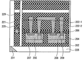
図1は赤外線固体撮像装置の上面図であり、図2は図1のA−A´における断面図である。図2において、シリコン基板201上に埋め込みシリコン酸化層202、SOI層203が順次積層されている。シリコン基板201には中空構造であるダイアフラム228が形成されており、赤外線を吸収することで発生した熱がシリコン基板201に逃げるのを防止する役割を果たす。SOI層203中には、トレンチ構造中に酸化シリコンが埋め込まれた、素子分離酸化膜204が形成されている。
1 is a top view of the infrared solid-state imaging device, and FIG. 2 is a cross-sectional view taken along line AA ′ of FIG. In FIG. 2, a buried
素子分離酸化膜204に挟まれたSOI層203の部分(熱電変換素子領域)の底部には、不純物濃度が4×1015cm-2であるp+電極領域207が形成される。p+電極領域207の上部には、導電型がp型で不純物濃度が1.5×1013cm-2であるpn接合ダイオード領域205が形成されており、この領域に熱電変換によって発生した電荷が蓄積する。そしてpn接合ダイオード領域205内であって、SOI層203表面の領域には、不純物濃度が5×1015cm-2であるn+電極領域206が形成され、このn+電極領域206表面からpn接合ダイオード領域205とn+電極領域206とで構成するpn接合ダイオードの一方の電極が引き出される。さらに、p+電極領域207に接続するように、不純物濃度が4×1015cm-2であるp+領域209が形成されている。このp+領域209上には、不純物濃度が2×1014cm-2であるp+コンタクト拡散層領域208が形成され、このp+コンタクト拡散層領域208の表面から上記pn接合ダイオードの他方の電極が引き出される。
A p + electrode region 207 having an impurity concentration of 4 × 10 15 cm −2 is formed at the bottom of the portion of the SOI layer 203 (thermoelectric conversion element region) sandwiched between the element
上記熱電変換素子領域が設けられていないSOI層203表面(これを「周辺領域」とする)には、ゲート210、側壁212とで構成された周辺回路212が形成されており、この周辺回路により、上記熱電変換素子領域で発生した電荷が読み出され、信号処理される。
On the surface of the
SOI層203上には、シリコン酸化膜からなる第一の層間絶縁膜221が形成される。第一の層間絶縁膜221中には、タングステン等の部材からなり、n+電極領域206に接続された第一コンタクト電極222−1、p+コンタクト拡散層領域208に接続された第二コンタクト電極222−2が形成されている。
A first interlayer
第一の層間絶縁膜221上には第二の層間絶縁膜224が形成され、その上部にはアルミニウムからなり、厚さが0.5〜0.6μmである可視光遮断層225が形成される。この可視光遮断層225はアルミニウム単層であってもよいが、可視光を完全に遮断するためには、例えば5nmのTiN、60nmのTi、0.5μmのAl、20nmのTiN、及び10nmのTiの積層構造であってもよい。可視光遮断層225上には、シリコン酸化膜226、シリコン窒化膜227がこの順で積層され、これらで赤外線吸収層228を構成する。
A second interlayer
図2の赤外線固体撮像装置によれば、赤外線吸収層228と熱電変換素子領域との間に厚さが0.5〜0.6μmである可視光遮断層225が形成されており、この層が熱電変換素子領域に可視光が入射するのを防止する役割を果たす。従来では、熱電変換素子領域に可視光が入射することで、熱電変換素子がフォトダイオード的な動作をし、pn接合ダイオード領域205に蓄積していた電荷が赤外線固体撮像装置固有の読み出しクロック以外のタイミングでn+電極領域206に向けて流出することによる、ダイオードの温度変化による電流上昇分が帳消しになっていた。そこで、本実施例では、pn接合ダイオードを構成する熱電変換素子領域の直上に可視光遮断層としてAlを挿入し、可視光、赤外線共に反射し、赤外線のみ上部の吸収膜にて吸収、熱に変換することにより、赤外線成分のみを信号として取り出す事ができる。
According to the infrared solid-state imaging device of FIG. 2, the visible
次に、本発明の実施例1の赤外線固体撮像装置の製造方法につき、図3乃至図10を用いて説明する。 Next, a method for manufacturing the infrared solid-state imaging device according to the first embodiment of the present invention will be described with reference to FIGS.
まず、図3に示すように、半導体基板として単結晶シリコン支持基板201上に埋め込みシリコン酸化膜層202、単結晶シリコン層203が順次積層された、いわゆるSOI基板200を準備する。
First, as shown in FIG. 3, a so-called
次に、図4に示すように、STI(Shallow−Trench−Isolation)構造により素子分離を行う。すなわち、フォトリソグラフィー技術により素子分離領域を規定し、素子分離領域の単結晶シリコン層203を、RIE(Reactive−Ion−Etching)によりエッチング除去した後に、素子分離酸化膜204をCVD(Chemical−Vapor−Deposition)により埋め込み、CMP(Chemical−Mechanical−Polishing)で平坦化する。このとき、図1における支持構造234の部分も素子分離領域として定義され、素子分離酸化膜204が埋め込まれる。
Next, as shown in FIG. 4, element isolation is performed using an STI (Shallow-Trench-Isolation) structure. That is, an element isolation region is defined by a photolithography technique, the single
素子分離酸化膜204形成後、図5に示すように、熱電変換素子となるpn接合ダイオードを形成する手段として、まずフォトリソグラフィー技術によりp型拡散層領域を規定し、イオン注入により、例えばホウ素を75keV、1.5×1013cm-2で注入し、pn接合ダイオード領域205を形成する。次に、同様にして、SOI層203の浅い領域にn+拡散層領域を規定し、例えばAsを40keV、5×1015cm-2で注入し、n+電極領域206を形成する。次に、同様にして、SOI層203の深い領域にp+電極領域207を、例えばBを7keV、4×1015cm-2で注入して形成し、基板表面に形成したp+コンタクト拡散層領域208と、これとp+電極領域207を接続する為に、基板深さ方向に伸張したp+領域209を形成する。これらの形成条件(イオン注入条件)としては、例えば、p+コンタクト拡散層領域208は、Bを130keV、2×1014cm-2であり、p+領域209は、Bを100keV、2.5×1013cm-2及び75keV、6×1013cm-2及び40keV、1.5×1013cm-2及び7keV、4×1015cm-2である。
After the element
次に、図6に示すように、ポリシリコン層210を形成した後に、フォトリソグラフィーとRIEによって支持構造234を加工する。本工程では周辺回路に使用するMOSトランジスタのゲート電極210も同時に形成される。その後シリコン窒化膜をCVDにより基板全面に形成し、RIEによりエッチバックする事により、ゲート電極および支持配線による段差部に側壁211形成する。この状態で、ゲート電極210、側壁211をマスクとしてイオン注入により、自己整合的にソースドレイン不純物領域を形成する。
Next, as shown in FIG. 6, after forming the
次に、図7に示すように、SOI層203全体にシリコン窒化膜をCVDにより堆積し、熱電変換素子領域におけるpn接合ダイオードのn+電極領域206、p+コンタクト領域208以外の領域にフォトマスクを形成し、シリコン窒化膜のRIEを行い、シリサイドブロック膜217を形成する。これにより、pn接合ダイオードのn+電極領域206、p+領域コンタクト208がシリサイドにより導通してしまうのを防ぐ。その後、ゲート電極、支持配線、側壁212およびシリサイドブロック膜217をマスクとして、ゲート絶縁膜を希弗酸等によりエッチングし、MOSトランジスタ213のゲート電極211、ソースドレイン領域、及び、pn接合ダイオードのn+電極領域206、p+コンタクト領域208のシリコン層を露出させる。次に、シリサイド形成のためのチタン膜218を全面に堆積する。この状態から、適当なアニール処理を行うことで、MOSトランジスタ213のゲート電極211、ソースドレイン領域、pn接合ダイオードのn+電極領域206、p+コンタクト領域208、および支持配線の露出シリコンは、チタン膜218と反応し、チタンシリサイド層219が形成される。チタンシリサイド層219形成後は硫酸と過酸化水素の混合液によって、シリサイド反応しない領域のチタン膜218を除去する。
Next, as shown in FIG. 7, a silicon nitride film is deposited on the
次に、図8に示すように、SOI層203全面にシリコン窒化膜220、シリコン酸化膜を材料とする第一の層間絶縁膜221をCVDにより堆積し、CMPにより平坦化を行う。
Next, as shown in FIG. 8, a
次に、図9に示すように、第一の層間絶縁膜221にコンタクトホール222をRIEにより形成し、CVDによりタングステンをSOI層203全面に堆積し、CMPを行う事で、コンタクトホールの埋め込みを行い、第一コンタクト電極222−1、第二コンタクト電極222−2を形成する。
Next, as shown in FIG. 9, contact holes 222 are formed in the first
次に、図10に示すように、アルミニウム合金を全面にスパッタ法により堆積し、フォトリソグラフィー技術とRIEによりパターニングし、第一コンタクト電極222−1、第二コンタクト電極222−2を接続する金属配線223を形成する。金属配線223形成後、第二の層間絶縁膜224としてシリコン酸化膜を堆積した後、可視光遮断層225としてAl膜を堆積し、熱電変換素子領域全面を覆うように形成する。可視光遮断層225としては、可視光に対して透過性の無いものならAlに限るものではなく、例えばAg、Al、Au、Rh、Cu、Tiやこれらの積層構造でも良い。また、可視光遮断層225として、LSIで用いられる配線層を流用すれば、プロセスを簡略化できる。この時の可視光遮断層225の構造としては、Alの上下の少なくとも一方にTiやTiN、或いはこれらの積層膜を配置した構造、またはCuの上下の少なくとも一方にTa、TaN、或いはこれらの積層膜を配置した構造が良い。その後、赤外線吸収層235としてシリコン酸化膜226とシリコン窒化膜227を堆積する。この時、赤外線吸収を十分に行うために、シリコン酸化膜226とシリコン窒化膜227の合計は0.5μm以上とする事が望ましい。
Next, as shown in FIG. 10, an aluminum alloy is deposited on the entire surface by sputtering, patterned by photolithography and RIE, and metal wiring for connecting the first contact electrode 222-1 and the second contact electrode 222-2. 223 is formed. After the
そして、ダイアフラム228形成の為のエッチングホール229をRIEにより形成し、シリコン基板201を露出させる。
Then, an
次に、TMAH(Tetra−Methyl−Ammonium−Hydroxide)によるシリコンに対する異方性ウエットエッチングにより、シリコン基板201内部にダイアフラム228を形成する。
Next, a
以上の工程により、図2に示す赤外線固体撮像装置が完成する。 Through the above steps, the infrared solid-state imaging device shown in FIG. 2 is completed.
なお、上述した各実施例は、この発明の技術的思想を具体化するための装置や方法を例示するものであって、この発明の技術的思想は、構成部品の材質、形状、構造、配置等を実施例に開示されたもののみに特定するものではない。本発明はその要旨を逸脱しない範囲で、種々変形して実施することができるものである。 Each of the above-described embodiments exemplifies an apparatus and a method for embodying the technical idea of the present invention. The technical idea of the present invention is based on the material, shape, structure, and arrangement of components. Etc. are not limited only to those disclosed in the embodiments. The present invention can be variously modified and implemented without departing from the spirit of the present invention.
200 … SOI基板
201 … シリコン基板
202 … 埋め込みシリコン酸化層
203 … SOI層
204 … 素子分離酸化膜
205 … pn接合ダイオード領域
206 … n+電極領域
207 … p+電極領域
208 … p+コンタクト拡散層領域
209 … p+領域
210 … ゲート電極
211 … 側壁
213 … MOSトランジスタ
217 … シリサイドブロック膜
218 … チタン膜
219 … チタンシリサイド層
220、227 … シリコン窒化膜
221 … 第一の層間絶縁膜
222 … コンタクトホール
222−1 … 第一コンタクト電極
222−2 … 第二コンタクト電極
223 … 金属配線
224 … 第二の層間絶縁膜
225 … 可視光遮断層
226 … シリコン酸化膜
228 … ダイアフラム
229 … エッチングホール
230 … 入力信号線
231 … 出力信号線
234 … 支持構造
235 … 赤外線吸収層
200 ...
Claims (5)
前記中空構造上部に形成され、前記赤外線吸収部で発生した熱による温度変化を電気信号に変換するpn接合ダイオードから構成される熱電変換部と、
前記赤外線吸収部と前記熱電変換部の間に存在し、かつ前記熱電変換部への可視光の入射を遮断する、厚さが0.5〜0.6μmである可視光遮断層と、
を具備する事を特徴とする赤外線固体撮像装置。 An infrared absorption part formed on the top of a semiconductor substrate having a hollow structure inside, for absorbing incident infrared rays and converting them into heat;
A thermoelectric conversion unit formed of a pn junction diode formed on the hollow structure and converting a temperature change due to heat generated in the infrared absorption unit into an electrical signal;
A visible light blocking layer having a thickness of 0.5 to 0.6 μm, which is present between the infrared absorption unit and the thermoelectric conversion unit and blocks visible light from entering the thermoelectric conversion unit;
An infrared solid-state imaging device characterized by comprising:
前記第一の半導体層内に形成される第一導電型の第一不純物領域と、
前記第一不純物領域中に形成される第二導電型の第二不純物領域と、
前記第一の半導体層上部に形成され、前記第一不純物領域及び前記第二不純物領域をそれぞれ接続する配線層と、
前記配線層上に形成され、厚さが0.5〜0.6μmである可視光遮断層と、
前記可視光遮断層上部に形成される、二層のそれぞれ材料の異なる絶縁層からなる赤外線吸収層と
を具備することを特徴とする赤外線固体撮像装置。 A first semiconductor layer formed on a semiconductor substrate having a hollow structure therein;
A first impurity region of a first conductivity type formed in the first semiconductor layer;
A second impurity region of a second conductivity type formed in the first impurity region;
A wiring layer formed on the first semiconductor layer and connecting the first impurity region and the second impurity region;
A visible light blocking layer formed on the wiring layer and having a thickness of 0.5 to 0.6 μm;
An infrared solid-state imaging device comprising: an infrared absorption layer formed of two insulating layers made of different materials, formed on the visible light blocking layer.
Priority Applications (1)
| Application Number | Priority Date | Filing Date | Title |
|---|---|---|---|
| JP2004272208A JP4410071B2 (en) | 2004-09-17 | 2004-09-17 | Infrared solid-state imaging device |
Applications Claiming Priority (1)
| Application Number | Priority Date | Filing Date | Title |
|---|---|---|---|
| JP2004272208A JP4410071B2 (en) | 2004-09-17 | 2004-09-17 | Infrared solid-state imaging device |
Publications (2)
| Publication Number | Publication Date |
|---|---|
| JP2006086465A JP2006086465A (en) | 2006-03-30 |
| JP4410071B2 true JP4410071B2 (en) | 2010-02-03 |
Family
ID=36164684
Family Applications (1)
| Application Number | Title | Priority Date | Filing Date |
|---|---|---|---|
| JP2004272208A Expired - Fee Related JP4410071B2 (en) | 2004-09-17 | 2004-09-17 | Infrared solid-state imaging device |
Country Status (1)
| Country | Link |
|---|---|
| JP (1) | JP4410071B2 (en) |
Cited By (1)
| Publication number | Priority date | Publication date | Assignee | Title |
|---|---|---|---|---|
| US10834343B2 (en) | 2016-11-08 | 2020-11-10 | Samsung Electronics Co., Ltd. | Image sensor including color splitting element and method of operating the image sensor |
Families Citing this family (2)
| Publication number | Priority date | Publication date | Assignee | Title |
|---|---|---|---|---|
| JP4904545B2 (en) * | 2007-06-01 | 2012-03-28 | 三菱電機株式会社 | Infrared solid-state imaging device and manufacturing method thereof |
| JP4975669B2 (en) * | 2008-03-25 | 2012-07-11 | 株式会社東芝 | Infrared detector and solid-state imaging device equipped with the infrared detector |
-
2004
- 2004-09-17 JP JP2004272208A patent/JP4410071B2/en not_active Expired - Fee Related
Cited By (1)
| Publication number | Priority date | Publication date | Assignee | Title |
|---|---|---|---|---|
| US10834343B2 (en) | 2016-11-08 | 2020-11-10 | Samsung Electronics Co., Ltd. | Image sensor including color splitting element and method of operating the image sensor |
Also Published As
| Publication number | Publication date |
|---|---|
| JP2006086465A (en) | 2006-03-30 |
Similar Documents
| Publication | Publication Date | Title |
|---|---|---|
| JP3717104B2 (en) | Photo detector with built-in circuit | |
| JP3497797B2 (en) | Manufacturing method of infrared sensor | |
| JP5501379B2 (en) | Solid-state imaging device and imaging system | |
| US8618458B2 (en) | Back-illuminated CMOS image sensors | |
| US7816752B2 (en) | Solid state imaging device and camera comprising a device isolation having a step | |
| US7943962B2 (en) | Solid-state image pickup device and method for producing the same | |
| US20070108476A1 (en) | Imager with reflector mirrors | |
| US20060243981A1 (en) | Masked spacer etching for imagers | |
| JPS63237583A (en) | Infrared sensor | |
| JP5264597B2 (en) | Infrared detector and infrared solid-state imaging device | |
| KR20020025681A (en) | Infrared sensor and method for manufacturing the same | |
| JP5546222B2 (en) | Solid-state imaging device and manufacturing method | |
| US20080194052A1 (en) | Optical semiconductor device and method for fabricating the same | |
| JP2009016729A (en) | Method for manufacturing pin photodiode | |
| JP2000124438A (en) | Solid-state image sensing device | |
| US20060270091A1 (en) | Pinned photodiode integrated with trench isolation and fabrication method | |
| JP5276908B2 (en) | Solid-state imaging device and manufacturing method thereof | |
| JP3672516B2 (en) | Infrared sensor device and manufacturing method thereof | |
| JP2011119558A (en) | Solid-state imaging device | |
| JP4028441B2 (en) | Infrared solid-state imaging device and manufacturing method thereof | |
| JP5143176B2 (en) | Infrared imaging device and manufacturing method thereof | |
| CN105575986A (en) | Solid-state imaging device and method of manufacturing solid-state imaging device | |
| JP4410071B2 (en) | Infrared solid-state imaging device | |
| US20050145905A1 (en) | Solid-state imaging device and production method of the same | |
| US6153446A (en) | Method for forming a metallic reflecting layer in a semiconductor photodiode |
Legal Events
| Date | Code | Title | Description |
|---|---|---|---|
| A131 | Notification of reasons for refusal |
Free format text: JAPANESE INTERMEDIATE CODE: A131 Effective date: 20090623 |
|
| A977 | Report on retrieval |
Free format text: JAPANESE INTERMEDIATE CODE: A971007 Effective date: 20090625 |
|
| A521 | Request for written amendment filed |
Free format text: JAPANESE INTERMEDIATE CODE: A523 Effective date: 20090812 |
|
| TRDD | Decision of grant or rejection written | ||
| A01 | Written decision to grant a patent or to grant a registration (utility model) |
Free format text: JAPANESE INTERMEDIATE CODE: A01 Effective date: 20091020 |
|
| A01 | Written decision to grant a patent or to grant a registration (utility model) |
Free format text: JAPANESE INTERMEDIATE CODE: A01 |
|
| A61 | First payment of annual fees (during grant procedure) |
Free format text: JAPANESE INTERMEDIATE CODE: A61 Effective date: 20091112 |
|
| FPAY | Renewal fee payment (event date is renewal date of database) |
Free format text: PAYMENT UNTIL: 20121120 Year of fee payment: 3 |
|
| LAPS | Cancellation because of no payment of annual fees |