EP1245086B1 - Bobine emettrice et receptrice - Google Patents
Bobine emettrice et receptrice Download PDFInfo
- Publication number
- EP1245086B1 EP1245086B1 EP01940609A EP01940609A EP1245086B1 EP 1245086 B1 EP1245086 B1 EP 1245086B1 EP 01940609 A EP01940609 A EP 01940609A EP 01940609 A EP01940609 A EP 01940609A EP 1245086 B1 EP1245086 B1 EP 1245086B1
- Authority
- EP
- European Patent Office
- Prior art keywords
- substrate plate
- coil
- plate
- substrate
- ferrite
- Prior art date
- Legal status (The legal status is an assumption and is not a legal conclusion. Google has not performed a legal analysis and makes no representation as to the accuracy of the status listed.)
- Expired - Lifetime
Links
Images
Classifications
-
- H—ELECTRICITY
- H04—ELECTRIC COMMUNICATION TECHNIQUE
- H04B—TRANSMISSION
- H04B5/00—Near-field transmission systems, e.g. inductive or capacitive transmission systems
- H04B5/40—Near-field transmission systems, e.g. inductive or capacitive transmission systems characterised by components specially adapted for near-field transmission
- H04B5/48—Transceivers
-
- G—PHYSICS
- G06—COMPUTING OR CALCULATING; COUNTING
- G06K—GRAPHICAL DATA READING; PRESENTATION OF DATA; RECORD CARRIERS; HANDLING RECORD CARRIERS
- G06K19/00—Record carriers for use with machines and with at least a part designed to carry digital markings
- G06K19/06—Record carriers for use with machines and with at least a part designed to carry digital markings characterised by the kind of the digital marking, e.g. shape, nature, code
- G06K19/067—Record carriers with conductive marks, printed circuits or semiconductor circuit elements, e.g. credit or identity cards also with resonating or responding marks without active components
- G06K19/07—Record carriers with conductive marks, printed circuits or semiconductor circuit elements, e.g. credit or identity cards also with resonating or responding marks without active components with integrated circuit chips
- G06K19/0723—Record carriers with conductive marks, printed circuits or semiconductor circuit elements, e.g. credit or identity cards also with resonating or responding marks without active components with integrated circuit chips the record carrier comprising an arrangement for non-contact communication, e.g. wireless communication circuits on transponder cards, non-contact smart cards or RFIDs
-
- H—ELECTRICITY
- H04—ELECTRIC COMMUNICATION TECHNIQUE
- H04B—TRANSMISSION
- H04B5/00—Near-field transmission systems, e.g. inductive or capacitive transmission systems
- H04B5/20—Near-field transmission systems, e.g. inductive or capacitive transmission systems characterised by the transmission technique; characterised by the transmission medium
- H04B5/24—Inductive coupling
- H04B5/26—Inductive coupling using coils
Definitions
- the invention relates to a communication element for an electro-magnetic coupling low-frequency communication system, comprising at least one transmitting and / or receiving electromagnetic field antenna in the form of a coil arranged on a substrate plate serving as a substrate. of support, this plate having a certain thickness.
- Such a low-frequency communication system by electromagnetic coupling is particularly used as a system of access and start-up called "hands-free" for a motor vehicle. It generally comprises an identification member mounted on board the vehicle and adapted to control the opening of the opening of the vehicle and the starting of the vehicle engine. It also comprises an identifier member intended to be worn by the user of the vehicle and which is able to communicate by electromagnetic coupling with the identifier member so that if the identifying member is recognized by the identifying member while the user is close to his vehicle, the opening of the vehicle is automatically opened and / or the vehicle engine is automatically started.
- the identifier member is generally an integral part of a flat badge or a key holder.
- the receiving antenna of this identifying member which is an electromagnetic coil is generally placed on a small interface box itself attached to the substrate plate.
- the object of the invention is to provide such a communication member whose electromagnetic field receiving coil is of a more compact form and can also be more sensitive, less expensive and more solid.
- the document DE 19 622 387 discloses a communication member as defined above, wherein the coil has turns which are wound in the thickness of the substrate plate. With this construction, the thickness of the communication member can be decreased by increasing the dimensions of the turns of the coil.
- the plate is provided with a recess and the coil is embedded in said recess.
- the turns of the coil are wound around the substrate plate and preferably the substrate plate is partially loaded with ferrite to form a core for the coil.
- the present invention proposes another embodiment which confers on the communication member an increased resistance to impacts which tend to separate the coil from the support plate.
- each turn of the coil is constituted by a conductive track on a first face of the substrate plate, a second conductive track on a second face of the substrate plate opposite to the first face and by two conducting bushings passing through. the thickness of the substrate plate and connecting the first and the second conductive track.
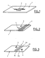
- the communication element comprises a substrate plate (printed circuit board) having a certain thickness and serving as a support for an electroconductive coil 2 forming the elocto-magnetic field receiving antenna of the communication.
- the coil 2 is embedded in a recess provided in the substrate plate. In this way, the coils of the coils are wound, preferably around a ferrite core, in the thickness of the substrate plate.
- the terminals 3 and 4 of the coils are etched on the substrate plate.
- the turns of the coil 2 are wound around the substrate plate 1 which is preferably partially filled with ferrite in the winding zone of the turns, or else be made of magnetic material or plasto-fist to constitute a core for the coil.
- the terminals 3, 4 of the coil are etched on the substrate plate.
- each turn of the coil 2 is constituted by a first conductive track 2A on a first face of the substrate plate by a second conductive track 2B on a second face of the substrate plate opposite to the first face and by two conductive vias 2C, 2D crossing the thickness of the substrate plate and connecting the first and second conductive track,
- the terminals 3 and 4 of the coil are still etched on the substrate plate 1.
- the plate substrate 1 may be partially loaded with ferrite in the winding area of the turns, or may be made of magnetic material or plasto-ferrite to form a core for the coil,
- the ferrite core of the coil 2 serves in particular to increase the inductance of the coil and therefore its sensitivity without increasing the thickness of the communication member.
Landscapes
- Engineering & Computer Science (AREA)
- Computer Networks & Wireless Communication (AREA)
- Signal Processing (AREA)
- Computer Hardware Design (AREA)
- Microelectronics & Electronic Packaging (AREA)
- Physics & Mathematics (AREA)
- General Physics & Mathematics (AREA)
- Theoretical Computer Science (AREA)
- Near-Field Transmission Systems (AREA)
- Coils Or Transformers For Communication (AREA)
Description
- L'invention porte sur un organe de communication pour système de communication basse fréquence par couplage électro-magnétlque, comprenant au moins une antenne émettrice et/ou réceptrice de champ électro-magnétique sous la forme d'une bobine disposée sur une plaque en substrat servant de support, cette plaque ayant une certaine épaisseur.
- Un tel système de communication basse fréquence par couplage électro-magnétique sert tout particulièrement comme système d'accès et de démarrage dit «mains libres » pour un véhicule automobile. Il comprend généralement un organe d'identification monté à bord du véhicule et apte à commander l'ouverture des ouvrants du véhicule ainsi que le démarrage du moteur du véhicule. II comprend aussi un organe identifiant destiné à être porté par l'utilisateur du véhicule et qui est apte à communiquer par couplage électro-magnétique avec l'organe Identificateur de telle sorte que si l'organe identificateur est reconnu par l'organe identifiant alors que l'utilisateur se trouve à proximité de son véhicule, les ouvrants du véhicule sont automatiquement ouverts et/ou le moteur du véhicule est automatiquement démarré.
- L'organe identifiant fait généralement partie Intégrante d'un badge plat ou d'un porte clé. L'antenne de réception de cet organe identifiant qui est une bobine électro-magnétique est généralement placée sur un petit boîtier interface lui-même fixé à la plaque en substrat
- Le but de l'invention est de proposer un tel organe de communication dont la bobine de réception du champs électro-magnétlque soit d'une forme plus compacte et puisse également être plus sensible, moins chère et plus solide.
- Le document
DE 19 622 387 décrit un organe de communication tel que défini plus haut, dans lequel la bobine a des spires qui sont enroulées dans l'épaisseur de la plaque en substrat. Avec cette construction, on peut diminuer l'épaisseur de l'organe de communication en augmentant la dimensions des spires de la bobine. - Selon un mode de réalisation de l'organe de communication selon, la plaque est munie d'un évidemment et la bobine est encastrée dans ledit évidemment.
- Selon encore un mode de réalisation de l'organe de communication les spires de la bobines sont enroulées autour de la plaque en substrat et de préférence la plaque en substrat est chargée partiellement en ferrite pour constituer un noyau pour la bobine.
- La présente invention propose un autre mode de réalisation qui confère à l'organe de communication une résistance accrue aux chocs qui tendent à désolidariser la bobine de la plaque support.
- Selon l'invention, chaque spire de la bobine est constituée par une piste conductrice sur une première face de la plaque en substrat, une seconde piste conductrice sur une seconde face de la plaque en substrat opposée à la première face et par deux traversées conductrices traversant l'épaisseur de la plaque en substrat et reliant la première et la seconde piste conductrice.
- Les exemples de réalisation ci-dessus de l'organe de communication selon l'invention sont décrits ci-après en détails et illustrés sur les dessins.
- Figure 1, l'organe de communication comprend une plaque en substrat (plaque de circuit imprimé) ayant une certaine épaisseur et servant de support à une bobine électro-conductrice 2 formant l'antenne de réception de champ élocto-magnétique de l'organe de communication. La bobine 2 est encastrée dans un évidemment prévu dans la plaque en substrat. De la sorte, les spires de la bobines sont enroulées, de préférence autour d'un noyau en ferrite, dans l'épaisseur de la plaque en substrat Les bornes 3 et 4 de la bobines sont gravées sur la plaque en substrat.
- Sur la figure 2. les spires de la bobine 2 sont enroulées autour de la plaque en substrat 1 qui est de préférence chargée partiellement en ferrite dans la zone d'enroulement des spires, ou encore être en matériau magnétique ou en plasto-fentte pour constituer un noyau pour la bobine. Les bornes 3, 4 de la bobine sont gravées sur la plaque en substrat.
- Sur la figure 3, chaque spire de la bobine 2 est constituée par une première piste conductrice 2A sur une première face de la plaque en substrat par une seconde piste conductrice 2B sur une seconde face de la plaque en substrat opposée à la première face et par deux traversées conductrices 2C,2D traversant l'épaisseur de la plaque en substrat et reliant la première et la seconde piste conductrice, Les bornes 3 et 4 de la bobine sont encore gravées sur la plaque en substrat 1. De même que précédemment, la plaque substrat 1 pourra être chargée partiellement en ferrite dans la zone d'enroulement des spires, ou encore être en materiau magnétique ou en plasto-ferrite pour constituer un noyau pour la bobine,
- Le noyau en ferrite de la bobine 2 sert en particulier à augmenter l'inductance de la bobine et donc sa sensibilité sans augmenter l'épaisseur de l'organe de communication.
Claims (3)
- Un organe de communication basse fréquence par couplage électro-magnétique, comprenant au moins une plaque en substrat (1) servant de support, cette plaque ayant une certaine épaisseur, et une antenne émettrice et/ou réceptrice de champ électro-magnétique sous la forme d'une bobine (2) comprenant des spires qui sont enroulées dans l'épaisseur de la plaque en substrat, caractérisé en ce que chaque spire de la bobine est constituée par une piste conductrice (2A) sur une première face de la plaque en substrat, une seconde piste conductrice (2B) sur une seconde face de la plaque en substrat opposée à la première face et par deux traversées conductrices (2C, 2D) traversant l'épaisseur de la plaque en substrat et reliant la première et la seconde piste conductrice.
- Organe selon la revendication 1, dans lequel la plaque en substrat est en matériau chargé partiellement en ferrite ou en matériau magnétique ou en plasto-ferrite pour constituer un noyau pour la bobine.
- Organe selon l'une quelconque des revendications précédentes, caractérisé en ce qu'il fait partie intégrante d'un badge plat ou d'un porte clé.
Applications Claiming Priority (3)
| Application Number | Priority Date | Filing Date | Title |
|---|---|---|---|
| FR0006040A FR2808943B1 (fr) | 2000-05-12 | 2000-05-12 | Identifiant pour systeme "d'acces et demarrage mains-libres" avec une bobine emettrice et/ou receptrice disposee dans l'epaisseur du substrat |
| FR0006040 | 2000-05-12 | ||
| PCT/FR2001/001486 WO2001086832A1 (fr) | 2000-05-12 | 2001-05-14 | Bobine emettrice et receptrice |
Publications (2)
| Publication Number | Publication Date |
|---|---|
| EP1245086A1 EP1245086A1 (fr) | 2002-10-02 |
| EP1245086B1 true EP1245086B1 (fr) | 2008-01-02 |
Family
ID=8850135
Family Applications (1)
| Application Number | Title | Priority Date | Filing Date |
|---|---|---|---|
| EP01940609A Expired - Lifetime EP1245086B1 (fr) | 2000-05-12 | 2001-05-14 | Bobine emettrice et receptrice |
Country Status (5)
| Country | Link |
|---|---|
| US (1) | US20020113747A1 (fr) |
| EP (1) | EP1245086B1 (fr) |
| DE (1) | DE60132166D1 (fr) |
| FR (1) | FR2808943B1 (fr) |
| WO (1) | WO2001086832A1 (fr) |
Families Citing this family (9)
| Publication number | Priority date | Publication date | Assignee | Title |
|---|---|---|---|---|
| US7098858B2 (en) * | 2002-09-25 | 2006-08-29 | Halliburton Energy Services, Inc. | Ruggedized multi-layer printed circuit board based downhole antenna |
| US7158754B2 (en) * | 2003-07-01 | 2007-01-02 | Ge Medical Systems Global Technology Company, Llc | Electromagnetic tracking system and method using a single-coil transmitter |
| JP4152845B2 (ja) * | 2003-09-22 | 2008-09-17 | 株式会社アルファ | アンテナ装置および該アンテナ装置を装着した自動車のドアアウトサイドハンドル装置 |
| US20050237241A1 (en) * | 2004-04-27 | 2005-10-27 | Garber Richard S | Antenna for radio frequency identification reader |
| FR2891091B1 (fr) * | 2005-09-22 | 2008-01-11 | Commissariat Energie Atomique | Antenne plane omnidirectionnelle et procede de fabrication |
| TW200826366A (en) * | 2006-11-02 | 2008-06-16 | Murata Manufacturing Co | Antenna coil and antenna unit |
| DE102015111038B4 (de) * | 2015-07-08 | 2021-05-06 | Infineon Technologies Ag | Eine vertikale Ferritantenne mit vorgefertigten Verbindungsbauteilen |
| DE202016007184U1 (de) * | 2016-11-22 | 2016-12-02 | Stadlbauer Marketing + Vertrieb Gmbh | Spulenanordnung und Modellauto mit einer derartigen Spulenandordnung |
| WO2025228789A1 (fr) * | 2024-05-01 | 2025-11-06 | Sonion Nederland B.V. | Ensemble bobine pour un récepteur et son procédé de production |
Family Cites Families (12)
| Publication number | Priority date | Publication date | Assignee | Title |
|---|---|---|---|---|
| US3683389A (en) * | 1971-01-20 | 1972-08-08 | Corning Glass Works | Omnidirectional loop antenna array |
| JPS5330976B1 (fr) * | 1971-07-22 | 1978-08-30 | ||
| US3719950A (en) * | 1971-11-03 | 1973-03-06 | A Bukhman | Antenna system for vhf and uhf radio direction finders |
| FR2443725B1 (fr) * | 1978-12-08 | 1985-11-29 | Rodrian James | Dispositif d'identification d'animaux |
| JP3891448B2 (ja) * | 1994-04-11 | 2007-03-14 | 日立金属株式会社 | 薄型アンテナおよびそれを用いたカード |
| KR100459839B1 (ko) * | 1995-08-22 | 2005-02-07 | 미쓰비시 마테리알 가부시키가이샤 | 트랜스폰더용안테나및트랜스폰더 |
| JPH0964797A (ja) * | 1995-08-28 | 1997-03-07 | Matsushita Electric Works Ltd | 移動体識別装置のカード型データキャリア |
| JPH09284029A (ja) * | 1996-04-16 | 1997-10-31 | Murata Mfg Co Ltd | チップアンテナ |
| DE19622387B4 (de) * | 1996-06-04 | 2004-04-15 | Aeg Identifikationssysteme Gmbh | Transponder |
| US6061030A (en) * | 1996-11-01 | 2000-05-09 | Plantronics, Inc. | Aerial arrays for magnetic induction communication systems having limited power supplies |
| DE19718423A1 (de) * | 1997-04-30 | 1998-11-05 | Siemens Ag | Tragbarer Signalempfänger |
| FR2792129B1 (fr) * | 1999-04-07 | 2006-07-28 | Valeo Securite Habitacle | Recepteur de signaux portable a plusieurs antennes |
-
2000
- 2000-05-12 FR FR0006040A patent/FR2808943B1/fr not_active Expired - Fee Related
-
2001
- 2001-05-04 US US10/030,261 patent/US20020113747A1/en not_active Abandoned
- 2001-05-14 EP EP01940609A patent/EP1245086B1/fr not_active Expired - Lifetime
- 2001-05-14 DE DE60132166T patent/DE60132166D1/de not_active Expired - Lifetime
- 2001-05-14 WO PCT/FR2001/001486 patent/WO2001086832A1/fr not_active Ceased
Also Published As
| Publication number | Publication date |
|---|---|
| FR2808943A1 (fr) | 2001-11-16 |
| WO2001086832A1 (fr) | 2001-11-15 |
| FR2808943B1 (fr) | 2004-10-01 |
| US20020113747A1 (en) | 2002-08-22 |
| EP1245086A1 (fr) | 2002-10-02 |
| DE60132166D1 (de) | 2008-02-14 |
Similar Documents
| Publication | Publication Date | Title |
|---|---|---|
| TWI258710B (en) | Antenna for reader/recorder and reader/recorder having the antenna | |
| CN101931123B (zh) | 天线装置 | |
| US6642896B2 (en) | Reader coil antenna, and non-contacting type card identification system using the same | |
| EP1288975A3 (fr) | Dispositif magnétique, son procédé de fabrication et alimentation équipée d'un tel dispositif | |
| JP2006050265A (ja) | アンテナモジュール用磁芯部材、アンテナモジュールおよびこれを備えた携帯情報端末 | |
| WO2002050848A3 (fr) | Inducteur plan avec plan conducteur segmente | |
| CA2405403A1 (fr) | Etiquette electronique | |
| JP2005340759A (ja) | アンテナモジュール用磁芯部材、アンテナモジュールおよびこれを備えた携帯情報端末 | |
| KR20150050541A (ko) | 무선 충전용 자기장 차폐시트 및 이를 구비하는 안테나 모듈 | |
| KR20170061580A (ko) | 안테나를 내장한 비접촉식 금속카드 | |
| CA2511244C (fr) | Systeme et procede anti-vol pour vehicule, et application de ce systeme pour la gestion d'une flotte de vehicules | |
| EP1221739A3 (fr) | Feuille pour pièces électroniques et méthode de sa fabrication | |
| KR20070004456A (ko) | 안테나, 및 이를 이용한 전파시계, 키리스 엔트리 시스템및 rfid 시스템 | |
| EP1245086A1 (fr) | Bobine emettrice et receptrice | |
| EP0917101B1 (fr) | Bobine d'antenne à champ électrique réduit | |
| EP1296332A3 (fr) | Mèmoire magnètique | |
| EP1592142A4 (fr) | Dispositif de communication et systeme de communication | |
| JP2002232321A (ja) | Rfidタグ及びその取付構造 | |
| JP3649502B2 (ja) | チョークコイル | |
| JP2002208814A (ja) | 通信装置及びその取付構造及び通信装置の情報読出方法 | |
| JP2008077140A (ja) | 非接触icタグ | |
| WO2002060041A3 (fr) | Bobine plate | |
| EP0763799A1 (fr) | Collecteur d'onde en forme de bobinage imprimé pour objet portatif électronique tel que carte ou badge sans contact | |
| EP1369546B1 (fr) | Module électronique flexible pour poignée d'ouvrant, notamment pour véhicule automobile | |
| JP4692217B2 (ja) | 非接触icカードリーダ装置 |
Legal Events
| Date | Code | Title | Description |
|---|---|---|---|
| PUAI | Public reference made under article 153(3) epc to a published international application that has entered the european phase |
Free format text: ORIGINAL CODE: 0009012 |
|
| AK | Designated contracting states |
Kind code of ref document: A1 Designated state(s): AT BE CH CY DE DK ES FI FR GB GR IE IT LI LU MC NL PT SE TR |
|
| 17P | Request for examination filed |
Effective date: 20020515 |
|
| RIN1 | Information on inventor provided before grant (corrected) |
Inventor name: BAUDARD, XAVIER Inventor name: TESSIER, VIRGINIE Inventor name: GASCHER, ALAIN |
|
| RAP1 | Party data changed (applicant data changed or rights of an application transferred) |
Owner name: VALEO SECURITE HABITACLE |
|
| RAP1 | Party data changed (applicant data changed or rights of an application transferred) |
Owner name: VALEO SECURITE HABITACLE S.A.S. |
|
| RBV | Designated contracting states (corrected) |
Designated state(s): DE ES FR GB IT |
|
| GRAP | Despatch of communication of intention to grant a patent |
Free format text: ORIGINAL CODE: EPIDOSNIGR1 |
|
| GRAS | Grant fee paid |
Free format text: ORIGINAL CODE: EPIDOSNIGR3 |
|
| GRAA | (expected) grant |
Free format text: ORIGINAL CODE: 0009210 |
|
| AK | Designated contracting states |
Kind code of ref document: B1 Designated state(s): DE ES FR GB IT |
|
| REG | Reference to a national code |
Ref country code: GB Ref legal event code: FG4D Free format text: NOT ENGLISH |
|
| REF | Corresponds to: |
Ref document number: 60132166 Country of ref document: DE Date of ref document: 20080214 Kind code of ref document: P |
|
| GBV | Gb: ep patent (uk) treated as always having been void in accordance with gb section 77(7)/1977 [no translation filed] | ||
| PG25 | Lapsed in a contracting state [announced via postgrant information from national office to epo] |
Ref country code: ES Free format text: LAPSE BECAUSE OF FAILURE TO SUBMIT A TRANSLATION OF THE DESCRIPTION OR TO PAY THE FEE WITHIN THE PRESCRIBED TIME-LIMIT Effective date: 20080413 |
|
| PLBE | No opposition filed within time limit |
Free format text: ORIGINAL CODE: 0009261 |
|
| STAA | Information on the status of an ep patent application or granted ep patent |
Free format text: STATUS: NO OPPOSITION FILED WITHIN TIME LIMIT |
|
| 26N | No opposition filed |
Effective date: 20081003 |
|
| PG25 | Lapsed in a contracting state [announced via postgrant information from national office to epo] |
Ref country code: GB Free format text: LAPSE BECAUSE OF FAILURE TO SUBMIT A TRANSLATION OF THE DESCRIPTION OR TO PAY THE FEE WITHIN THE PRESCRIBED TIME-LIMIT Effective date: 20080102 |
|
| PG25 | Lapsed in a contracting state [announced via postgrant information from national office to epo] |
Ref country code: DE Free format text: LAPSE BECAUSE OF FAILURE TO SUBMIT A TRANSLATION OF THE DESCRIPTION OR TO PAY THE FEE WITHIN THE PRESCRIBED TIME-LIMIT Effective date: 20080403 |
|
| PG25 | Lapsed in a contracting state [announced via postgrant information from national office to epo] |
Ref country code: IT Free format text: LAPSE BECAUSE OF FAILURE TO SUBMIT A TRANSLATION OF THE DESCRIPTION OR TO PAY THE FEE WITHIN THE PRESCRIBED TIME-LIMIT Effective date: 20080102 |
|
| REG | Reference to a national code |
Ref country code: FR Ref legal event code: PLFP Year of fee payment: 16 |
|
| REG | Reference to a national code |
Ref country code: FR Ref legal event code: PLFP Year of fee payment: 17 |
|
| REG | Reference to a national code |
Ref country code: FR Ref legal event code: PLFP Year of fee payment: 18 |
|
| PGFP | Annual fee paid to national office [announced via postgrant information from national office to epo] |
Ref country code: FR Payment date: 20180528 Year of fee payment: 18 |
|
| PG25 | Lapsed in a contracting state [announced via postgrant information from national office to epo] |
Ref country code: FR Free format text: LAPSE BECAUSE OF NON-PAYMENT OF DUE FEES Effective date: 20190531 |