EP1239525A2 - Piezokeramische Vielschichtaktoren sowie ein Verfahren zu ihrer Herstellung - Google Patents
Piezokeramische Vielschichtaktoren sowie ein Verfahren zu ihrer Herstellung Download PDFInfo
- Publication number
- EP1239525A2 EP1239525A2 EP02003957A EP02003957A EP1239525A2 EP 1239525 A2 EP1239525 A2 EP 1239525A2 EP 02003957 A EP02003957 A EP 02003957A EP 02003957 A EP02003957 A EP 02003957A EP 1239525 A2 EP1239525 A2 EP 1239525A2
- Authority
- EP
- European Patent Office
- Prior art keywords
- actuator
- grooves
- piezoceramic multilayer
- piezoceramic
- layer
- Prior art date
- Legal status (The legal status is an assumption and is not a legal conclusion. Google has not performed a legal analysis and makes no representation as to the accuracy of the status listed.)
- Granted
Links
Images


Classifications
-
- H—ELECTRICITY
- H10—SEMICONDUCTOR DEVICES; ELECTRIC SOLID-STATE DEVICES NOT OTHERWISE PROVIDED FOR
- H10N—ELECTRIC SOLID-STATE DEVICES NOT OTHERWISE PROVIDED FOR
- H10N30/00—Piezoelectric or electrostrictive devices
- H10N30/01—Manufacture or treatment
- H10N30/05—Manufacture of multilayered piezoelectric or electrostrictive devices, or parts thereof, e.g. by stacking piezoelectric bodies and electrodes
- H10N30/053—Manufacture of multilayered piezoelectric or electrostrictive devices, or parts thereof, e.g. by stacking piezoelectric bodies and electrodes by integrally sintering piezoelectric or electrostrictive bodies and electrodes
-
- H—ELECTRICITY
- H10—SEMICONDUCTOR DEVICES; ELECTRIC SOLID-STATE DEVICES NOT OTHERWISE PROVIDED FOR
- H10N—ELECTRIC SOLID-STATE DEVICES NOT OTHERWISE PROVIDED FOR
- H10N30/00—Piezoelectric or electrostrictive devices
- H10N30/01—Manufacture or treatment
- H10N30/08—Shaping or machining of piezoelectric or electrostrictive bodies
- H10N30/085—Shaping or machining of piezoelectric or electrostrictive bodies by machining
- H10N30/088—Shaping or machining of piezoelectric or electrostrictive bodies by machining by cutting or dicing
-
- H—ELECTRICITY
- H10—SEMICONDUCTOR DEVICES; ELECTRIC SOLID-STATE DEVICES NOT OTHERWISE PROVIDED FOR
- H10N—ELECTRIC SOLID-STATE DEVICES NOT OTHERWISE PROVIDED FOR
- H10N30/00—Piezoelectric or electrostrictive devices
- H10N30/50—Piezoelectric or electrostrictive devices having a stacked or multilayer structure
- H10N30/508—Piezoelectric or electrostrictive devices having a stacked or multilayer structure adapted for alleviating internal stress, e.g. cracking control layers
-
- Y—GENERAL TAGGING OF NEW TECHNOLOGICAL DEVELOPMENTS; GENERAL TAGGING OF CROSS-SECTIONAL TECHNOLOGIES SPANNING OVER SEVERAL SECTIONS OF THE IPC; TECHNICAL SUBJECTS COVERED BY FORMER USPC CROSS-REFERENCE ART COLLECTIONS [XRACs] AND DIGESTS
- Y10—TECHNICAL SUBJECTS COVERED BY FORMER USPC
- Y10T—TECHNICAL SUBJECTS COVERED BY FORMER US CLASSIFICATION
- Y10T29/00—Metal working
- Y10T29/42—Piezoelectric device making
Definitions
- the invention relates to piezoceramic multilayer actuators and a method their manufacture.
- Piezoceramic multilayer actuators are manufactured as monoliths, that is, the active material on which before sintering through a screen printing process Inner electrodes are applied as a so-called green film to one Stacked on top of each other, which is pressed into a green body. The Pressing the green body is usually done by lamination under pressure and Temperature effects performed in laminating molds.
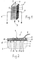
- a piezoceramic multi-layer actuator 1 produced in this way is strong in FIG schematically shown enlarged.
- the actuator consists of stacked thin ones Layers 2 of piezoelectrically active material, for example lead zirconate titanate (PZT), with conductive internal electrodes 3 arranged between them alternately to the actuator surface.
- External electrodes 4, 5 connect the inner electrodes 3. This makes the inner electrodes 3 electrical connected in parallel and combined into two groups.
- the two External electrodes 4, 5 are the connection poles of the actuator 1. They are over the Connections 6 connected to a voltage source, not shown here.
- FIG. 2 shows a section through the outer electrode 4 and the surface of the Piezoceramic multilayer actuator 1 according to the prior art.
- the figure shows the structure of an outer electrode.
- On to a stack pressed thin layers 2 of the piezoelectrically active material is in Area of the led out to the surface 10 of the multi-layer actuator 1
- Internal electrodes 3 for example by galvanic processes or screen printing of metal paste, a base metallization 11 for connecting the same polarity Inner electrodes 3 applied.
- This basic metallization 11 is by a another layer 12 reinforced from a metallic material, for example through a structured sheet or a wire mesh.
- the connection of the Reinforcement layer 12 with the base metallization 11 takes place by means of a Connection layer 13, usually a solder layer.
- the reinforcement layer 12, the electrical connection wire 6 is soldered.
- the cracks 15 generally run from the brittle and low-tensile base metallization 11 into the insulating region 14 and are caught there by regions with high tensile stresses, preferably at the electrode tips 16 of the electrodes 3 not touching the base metallization 11, or they begin in the areas of maximum tensile stress at the electrode tips 16 and run in the direction of the base metallization 11.
- the propagation of a crack 17 along an inner electrode 3 touching the base metallization 11 is to be classified as uncritical, since such a crack profile does not impair the function of the actuator.
- Cracks 15, on the other hand, which run uncontrolled through the insulation area 14 are very critical, since they reduce the insulation distance and greatly increase the probability of actuator failure due to flashovers.
- the object of the invention is to design the multi-layer actuators so that the in avoid the causes leading to the formation of cracks as far as possible become.
- the problem is solved by the fact that on the surface of the inactive Area, the isolation area, by the surface interrupting ablation a structure is created.
- the basic metallization is exclusively on the remaining surface applied by the structure.
- This is the Outer electrode not covering the entire surface of the multi-layer actuator connected and the rigidity of the composite, consisting of the surface of the Isolation area, the base metallization, the connection layer and the Reinforcement layer is reduced.
- the structuring causes the mechanical reaction of the outer electrode to the actuator is reduced.
- the Tensile stresses occurring in the insulation area can no longer become one add up critical size, which is the strength of the ceramic material exceeds and discharges in cracks.
- the thickness of the isolation area also depends on the size of the actuator. at full exploitation of the thickness of the isolation area, the depth of the Structure, the depth of the ablation, approximately up to 0.5 mm.
- the structure of an actuator can be green as well as sintered Condition. Editing in the green state is the more advantageous because of it is gentler on the tool due to the even softer ceramic material and also carried out with methods other than the usual grinding method can be. Another advantage is that when sintering sintered skin created covers the structure introduced into the green body and isolated. This makes it reliable against electrical flashovers and Protected against moisture.
- Interrupting the surface of the insulation area by abrasion can be easily done by anyone accomplish cutting machining processes.
- an actuator also offers machining with one suitable laser. The one machined by grinding after sintering However, the surface must be subsequently insulated, for example with a Polymeric material.
- the width of a groove, the distance between two grooves and the angle of this Grooves in relation to the longitudinal axis of the actuator must be coordinated with one another that no more than a certain number of internal electrodes between two grooves on the actuator surface. This maximum number depends on the specific elongation of the actuator during operation and the strength of the ceramic material.
- the grooves can be spaced from 0.2 mm to 10 mm arranged to match the size of the actuator. As special A distance of approximately five layers of between two grooves has been suitable Internal electrodes or a distance of about 0.8 mm to 1.2 mm proved. Will the The number of internal electrodes selected too high, so add up Tensile stresses from electrode to electrode and exceed the critical Value that leads to crack formation.
- the grooves can be at an angle of 0 degrees to 80 degrees to the longitudinal axis of the Be arranged actuator. At 0 degrees, the grooves run parallel to the longitudinal axis of the actuator. A range of 50 degrees to 30 degrees is advantageous. Is considered Cutting angle selected, for example, 45 °, result as favorable parameters a distance between two grooves and a width of the grooves of about 0.7 mm, about 1mm / ⁇ 2.
- a Multi-layer actuator according to the invention described.
- a low sintering Piezoceramic material for example that from DE 198 40 488 A1 known SKN53, is made with an organic binder as 125 ⁇ m thick Green film prepared.
- An inner electrode paste is applied to this green sheet Silver-palladium powder with a weight ratio of the proportions of 70/30 and a suitable binder applied by screen printing.
- a variety such green foils are stacked on top of each other in a block and under the laminated known conditions of pressure and temperature. From the laminate the individual rod-shaped actuators are separated.
- each one Multi-layer actuator 1 in a machining process, for example with a side milling cutter, on the sides to be contacted below a suitable angle 25 to the longitudinal axis 23 of the actuator 1 grooves 20 with a milled to a depth 24 such that the inactive insulating region 14 is completely severed becomes.
- the milling of the grooves 20 is repeated at regular intervals 21.
- the resulting interruptions 19 in the surface 10 of the actuator form a structure 18 in the form of parallel strips, as shown in FIG.
- FIG. 3 shows the non-metallized surface 10 of the actuator on which the course of the surface 10 Inner electrodes 3 and the course of the grooves 20 can be tracked.
- the base metallization On the surface 10 of the actuator 1 that remains due to the structuring 18, as can be seen in FIG. 4, the base metallization by means of a printing process 11 applied from a silver-containing baking paste. After branding the Base metallization 11, the outer electrodes are soldered on Metal wire mesh completed.
- the actuators prepared in this way in the green state become at about 400 ° C pyrolyzed and sintered at about 1100 ° C.
- the first variant Actuator base body with a cross-sectional area of 12.50 mm x 12.50 mm and 37.50 mm length produced as a green body.
- the thickness of a single ceramic layer, a green sheet, was 125 microns, the thickness of the metallization Inner electrode 3 ⁇ m.
- This variant served as a reference sample and represented the state of the art.
- the second variant Actuator base body with a cross-sectional area of 12.50 mm x 12.50 mm and 37.50 mm length produced as a green body.
- the thickness of a single ceramic layer, a green sheet, was 125 microns, the thickness of the metallization Inner electrode 3 ⁇ m.
- the actuator base body was on the one External electrode to be contacted with a side milling cutter with 0.7 mm Cutting width at an angle of 45 ° to the actuator longitudinal axis in regular Intervals milled.
- the depth of the grooves of 0.5 mm corresponded to the thickness of the Isolating.
- the distance between the grooves was 0.7 mm in each case.
- the third variant Actuator base body with a cross-sectional area of 12.50 mm x 12.50 mm and 37.50 mm length produced as a green body.
- the thickness of a single ceramic layer, a green sheet, was 125 microns, the thickness of the metallization Inner electrode 3 ⁇ m.
- the actuator base body was on the to be contacted Sides with a side milling cutter with a cutting width of 0.2 mm at an angle of Routed 90 ° to the longitudinal axis of the actuator at regular intervals.
- the depth of the Grooves of 0.5 mm corresponded to the thickness of the insulation area.
- the distance between the grooves were 1.0 mm each.
- the course of the grooves in this test corresponds not the course envisaged in practice, because through it one of the Groove width dependent number of internal electrodes that led to the surface are milled away and not connected to the outer electrode.
- the Groove course was chosen because the grooves act like notches and therefore with the Longitudinal expansion of an actuator has the most unfavorable effect on its tensile strength to have. It should be examined what additional effects may be cracks that may appear on the structure of the surface.
- the fourth variant was a Bodies with a cross-sectional area of 100 mm x 12.50 mm and 37.50 mm Length produced as a green body, which after creating the structure in eight individual rod-shaped actuator body was disassembled.
- the thickness of one Ceramic single layer, a green sheet was 125 ⁇ m, the thickness of the Metallization layer of the inner electrode 3 ⁇ m.
- the actuator bolts were on the sides to be contacted with a side milling cutter with 0.7 mm cutting width at an angle of 45 ° to the actuator's longitudinal axis at regular intervals milled.
- the depth of the grooves of 0.5 mm corresponded to the thickness of the Isolating.
- the distance between the grooves was 0.7 mm in each case.
- the actuator base body of the above four exemplary embodiments was approximately Pyrolysed 400 ° C and then sintered at about 1100 ° C.
- the fifth variant Actuator base body with a cross-sectional area of 12.50 mm x 12.50 mm and 37.50 mm length produced as a green body.
- the thickness of a single ceramic layer, a green sheet, was 125 microns, the thickness of the metallization Inner electrode 3 ⁇ m.
- the actuator bodies were pyrolyzed and sintered. First afterwards, cuts were made on the sides to be contacted with a diamond saw with a cutting width of 0.2 mm at an angle of 45 ° to the longitudinal axis of the actuator in milled in at regular intervals.
- the depth of the grooves corresponded to 0.4 mm the thickness of the isolation area.
- the distance between the grooves was 0.6 mm. After careful cleaning, the grooves were filled with a silicone resin.
- the Resin was cured at 140 ° C.
- the outer electrodes which consisted of a wire mesh, were soldered onto the actuator bodies of the five variants using a known method.
- the material of the network was a material adapted to the thermal expansion coefficient of the ceramic material, for example FeNi 36 .
- the wire diameter was 100 ⁇ m, the mesh size 200 ⁇ m.
- the network was pre-treated, for example copper-plated, to enable solderability. SnAg 4 was used as the solder.
- the soldering time was 2 minutes at 240 ° C.
- the multilayer actuators thus produced were cleaned and cleaned with a suitable one Paintwork isolated. After soldering connection wires to the Electrode networks, the actuators were preloaded in test frames with 2000 N and controlled with a trapezoidal signal. The control voltage was 100 ⁇ s raised from 0 V to 200 V, held at 200 V for 1 ms, and then in 100 ⁇ s reduced to 0 V. The repetition frequency was 200 Hz. The actuators reached operating temperatures from 150 to 160 ° C.
Landscapes
- Engineering & Computer Science (AREA)
- Manufacturing & Machinery (AREA)
- General Electrical Machinery Utilizing Piezoelectricity, Electrostriction Or Magnetostriction (AREA)
- Micromachines (AREA)
- Fuel-Injection Apparatus (AREA)
- Laminated Bodies (AREA)
- Supporting Of Heads In Record-Carrier Devices (AREA)
Abstract
Description
Claims (26)
- Piezokeramischer Vielschichtaktor (1) mit alternierend an sich gegenüberliegenden Oberflächen (10) des Aktors (1) geführte Innenelektroden (3), die auf der jeweiligen Oberfläche (10) durch eine Außenelektrode (4, 5) miteinander verbunden sind, die mindestens aus einer auf dem inaktiven Bereich (14) des Aktors (1) aufgetragenen Schicht einer Grundmetallisierung (11) besteht, mit der mittels einer Verbindungsschicht (13) eine Verstärkungsschicht (12) verbunden ist, an der ein Anschluss (6) zu einer Spannungsquelle angelötet sein kann, dadurch gekennzeichnet, dass die Oberfläche (10) des Vielschichtaktors (1) im inaktiven Bereich (14) eine Struktur (18) aufweist, die durch die Oberfläche (10) unterbrechende Abtragungen (19) erzeugt ist und dass die Grundmetallisierung (11) ausschließlich auf der durch die Struktur (18) verbliebenen Oberfläche (10) aufgetragen ist.
- Piezokeramischer Vielschichtaktor nach Anspruch 1 dadurch gekennzeichnet, dass die Tiefe (24) der die Struktur (18) erzeugenden Abtragungen (19) an der Oberfläche (10) des Aktors (1) der Dicke des Isolierbereichs (14) entspricht.
- Piezokeramischer Vielschichtaktor nach Anspruch 1 oder 2, dadurch gekennzeichnet, dass die Tiefe (24) der Struktur (18) bis etwa 0,5 mm beträgt.
- Piezokeramischer Vielschichtaktor nach einem der Ansprüche 1 bis 3, dadurch gekennzeichnet, dass die die Struktur (18) erzeugenden Abtragungen (19) der Oberfläche (10) des Aktors (1) aus Nuten (20) besteht.
- Piezokeramischer Vielschichtaktor nach Anspruch 4, dadurch gekennzeichnet, dass die Nuten (20) parallel zueinander angeordnet sind.
- Piezokeramischer Vielschichtaktor nach Anspruch 4 oder 5, dadurch gekennzeichnet, dass die Breite (22) einer Nut (20), der Abstand (21) zwischen zwei Nuten (20) und der Winkel (25) dieser Nuten (20) gegenüber der Längsachse (23) des Aktors (1) so aufeinander abgestimmt sind, dass nicht mehr als eine vorgegebene Anzahl von Innenelektroden (3) zwischen zwei Nuten an die Oberfläche (10) des Aktors tritt.
- Piezokeramischer Vielschichtaktor nach einem der Ansprüche 4 bis 6, dadurch gekennzeichnet, dass die Breite (22) der Nuten (20) 0,2 mm bis 2 mm, vorzugsweise 0,2 mm bis 0,7 mm beträgt.
- Piezokeramischer Vielschichtaktor nach einem der Ansprüche 4 bis 7, dadurch gekennzeichnet, dass die Nuten (20) in einem Abstand (21) von 0,2 mm bis 10 mm angeordnet sind.
- Piezokeramischer Vielschichtaktor nach einem der Ansprüche 6 bis 8, dadurch gekennzeichnet, dass die optimale Anzahl von Innenelektroden (3), die zwischen zwei Nuten an die Oberfläche (10) des Aktors tritt, etwa fünf ist und damit der Abstand der Nuten (20) voneinander etwa 0,8 mm bis 1,2 mm beträgt.
- Piezokeramischer Vielschichtaktor nach einem der Ansprüche 4 bis 9, dadurch gekennzeichnet, dass die Nuten (20) in einem Winkel von 0 Grad bis 80 Grad, vorzugsweise von 30 Grad bis 50 Grad, zur Längsachse (23) des Aktors (1) verlaufen.
- Piezokeramischer Vielschichtaktor nach einem der Ansprüche 4 bis 10, dadurch gekennzeichnet, dass die Struktur (18) ein Gitter (26) aus sich kreuzenden Nuten (20) ist.
- Piezokeramischer Vielschichtaktor nach einem der Ansprüche 1 bis 11, dadurch gekennzeichnet, dass die Struktur (18) durch ein spangebendes Bearbeitungsverfahren erzeugt ist.
- Piezokeramischer Vielschichtaktor nach einem der Ansprüche 1 bis 11, dadurch gekennzeichnet, dass die Struktur (18) durch ein Laserverfahren erzeugt ist.
- Piezokeramischer Vielschichtaktor nach einem der Ansprüche 1 bis 13, dadurch gekennzeichnet, dass die Struktur (18) im Grünzustand des Aktors (1) in die Oberfläche (10) eingebracht ist.
- Piezokeramischer Vielschichtaktor nach einem der Ansprüche 1 bis 13, dadurch gekennzeichnet, dass die Struktur (18) im gesinterten Zustand des Aktors (1) in die Oberfläche (10) eingebracht ist.
- Verfahren zur Herstellung eines piezokeramischen Vielschichtaktors nach einem der Ansprüche 1 bis 15, dadurch gekennzeichnet, dass auf der Oberfläche des inaktiven Bereichs des Aktors durch Abtragungen der Oberfläche eine Struktur erzeugt wird und dass die Grundmetallisierung zur Verbindung der Innenelektroden ausschließlich auf der durch die Struktur verbliebenen Oberfläche aufgetragen wird.
- Verfahren nach Anspruch 16, dadurch gekennzeichnet, dass zur Erzeugung der Struktur die Oberfläche in einer Dicke abgetragen wird, die der Dicke des Isolierbereichs entspricht.
- Verfahren nach einem der Ansprüche 16 oder 17, dadurch gekennzeichnet, dass in der Oberfläche des Aktors Nuten erzeugt werden.
- Verfahren nach Anspruch 18, dadurch gekennzeichnet, dass die Nuten parallel angeordnet werden.
- Verfahren nach Anspruch 18 oder 19, dadurch gekennzeichnet, dass die Breite einer Nut, der Abstand zwischen zwei Nuten und der Winkel dieser Nuten gegenüber der Längsachse des Aktors so aufeinander abgestimmt werden, dass nicht mehr als eine vorgegebene Anzahl von Innenelektroden zwischen zwei Nuten an die Oberfläche des Aktors tritt.
- Verfahren nach Anspruch 20, dadurch gekennzeichnet, dass die Anzahl von Innenelektroden, die zwischen zwei Nuten an die Oberfläche des Aktors tritt, mit fünf festgelegt wird.
- Verfahren nach einem der Ansprüche 18 bis 20, dadurch gekennzeichnet, dass eine Gitterstruktur durch sich kreuzende Nuten erzeugt wird.
- Verfahren nach einem der Ansprüche 16 bis 22, dadurch gekennzeichnet, dass die Struktur durch ein spangebendes Bearbeitungsverfahren erzeugt wird.
- Verfahren nach einem der Ansprüche 16 bis 22, dadurch gekennzeichnet, dass die Struktur durch ein Laserverfahren erzeugt wird.
- Verfahren nach einem der Ansprüche 16 bis 24, dadurch gekennzeichnet, dass die Struktur im Grünzustand des Aktors erzeugt wird.
- Verfahren nach einem der Ansprüche 16 bis 24, dadurch gekennzeichnet, dass die Struktur im gesinterten Zustand des Aktors erzeugt wird.
Applications Claiming Priority (4)
| Application Number | Priority Date | Filing Date | Title |
|---|---|---|---|
| DE10110617 | 2001-03-06 | ||
| DE10110617 | 2001-03-06 | ||
| DE10206115 | 2002-02-13 | ||
| DE10206115A DE10206115A1 (de) | 2001-03-06 | 2002-02-13 | Piezokeramische Vielschichtaktoren sowie ein Verfahren zu ihrer Herstellung |
Publications (3)
| Publication Number | Publication Date |
|---|---|
| EP1239525A2 true EP1239525A2 (de) | 2002-09-11 |
| EP1239525A3 EP1239525A3 (de) | 2005-08-31 |
| EP1239525B1 EP1239525B1 (de) | 2007-09-12 |
Family
ID=26008683
Family Applications (1)
| Application Number | Title | Priority Date | Filing Date |
|---|---|---|---|
| EP02003957A Expired - Lifetime EP1239525B1 (de) | 2001-03-06 | 2002-02-22 | Piezokeramische Vielschichtaktoren sowie ein Verfahren zu ihrer Herstellung |
Country Status (6)
| Country | Link |
|---|---|
| US (1) | US6731050B2 (de) |
| EP (1) | EP1239525B1 (de) |
| JP (1) | JP2002280630A (de) |
| AT (1) | ATE373321T1 (de) |
| DE (2) | DE10206115A1 (de) |
| DK (1) | DK1239525T3 (de) |
Cited By (3)
| Publication number | Priority date | Publication date | Assignee | Title |
|---|---|---|---|---|
| WO2003073523A3 (de) * | 2002-02-22 | 2004-02-19 | Epcos Ag | Piezoaktor mit strukturierter aussenelektrode |
| DE102004047105A1 (de) * | 2004-09-29 | 2006-05-24 | Robert Bosch Gmbh | Piezoaktor mit spannungsabbauenden Strukturen |
| WO2015082399A1 (de) * | 2013-12-04 | 2015-06-11 | Robert Bosch Gmbh | Piezoaktor und steuerventil mit einem solchen piezoaktor |
Families Citing this family (16)
| Publication number | Priority date | Publication date | Assignee | Title |
|---|---|---|---|---|
| WO1999008330A1 (de) * | 1997-08-05 | 1999-02-18 | Siemens Aktiengesellschaft | Vorgespannter piezoelektrischer aktor |
| DE10055241A1 (de) * | 2000-11-08 | 2002-05-29 | Epcos Ag | Piezoaktor |
| DE10205928A1 (de) * | 2001-02-21 | 2002-08-22 | Ceramtec Ag | Verfahren zur Herstellung piezokeramischer Vielschichtaktoren |
| DE10234787C1 (de) * | 2002-06-07 | 2003-10-30 | Pi Ceramic Gmbh Keramische Tec | Verfahren zur Herstellung eines monolithischen Vielschichtaktors, monolithischer Vielschichtaktor aus einem piezokeramischen oder elektrostriktiven Material |
| US6988706B2 (en) * | 2003-12-17 | 2006-01-24 | General Electric Company | Piezoelectric microvalve |
| WO2005064700A1 (ja) * | 2003-12-26 | 2005-07-14 | Murata Manufacturing Co., Ltd | 厚膜電極、及び積層セラミック電子部品 |
| JP4847039B2 (ja) * | 2004-05-28 | 2011-12-28 | 日本碍子株式会社 | 圧電/電歪構造体及び圧電/電歪構造体の製造方法 |
| US7176602B2 (en) * | 2004-10-18 | 2007-02-13 | Ssi Technologies, Inc. | Method and device for ensuring trandsducer bond line thickness |
| JP4723874B2 (ja) * | 2005-02-18 | 2011-07-13 | 花王株式会社 | 染毛剤組成物 |
| JP4936306B2 (ja) * | 2006-01-13 | 2012-05-23 | 日本碍子株式会社 | 積層型圧電素子およびその製造方法 |
| DE102006011293A1 (de) * | 2006-03-10 | 2007-09-13 | Siemens Ag | Piezoaktor und Verfahren zum Herstellen eines Piezoaktors |
| DE102006018056A1 (de) * | 2006-04-19 | 2007-10-31 | Robert Bosch Gmbh | Piezoaktor mit außen kontaktierten Innenelektroden eines Piezoelements |
| JP4911066B2 (ja) * | 2007-02-26 | 2012-04-04 | 株式会社デンソー | 積層型圧電素子 |
| CN101911325B (zh) * | 2007-12-26 | 2013-05-15 | 京瓷株式会社 | 层叠型压电元件、利用该元件的喷射装置及燃料喷射系统 |
| US11309481B2 (en) * | 2018-01-30 | 2022-04-19 | Taiyo Yuden Co., Ltd | Multi-layer piezoelectric ceramic component-mounted piezoelectric device |
| JP7036604B2 (ja) * | 2018-01-30 | 2022-03-15 | 太陽誘電株式会社 | 積層圧電セラミック部品及び圧電デバイス |
Family Cites Families (9)
| Publication number | Priority date | Publication date | Assignee | Title |
|---|---|---|---|---|
| JP3041952B2 (ja) * | 1990-02-23 | 2000-05-15 | セイコーエプソン株式会社 | インクジェット式記録ヘッド、圧電振動体、及びこれらの製造方法 |
| JP2545639B2 (ja) * | 1990-07-30 | 1996-10-23 | 富士通株式会社 | 積層型圧電素子 |
| JPH04214686A (ja) * | 1990-10-05 | 1992-08-05 | Nec Corp | 電歪効果素子 |
| US5406164A (en) * | 1993-06-10 | 1995-04-11 | Brother Kogyo Kabushiki Kaisha | Multilayer piezoelectric element |
| DE19648545B4 (de) * | 1996-11-25 | 2009-05-07 | Ceramtec Ag | Monolithischer Vielschichtaktor mit Außenelektroden |
| DE19753930A1 (de) * | 1997-12-05 | 1999-06-10 | Ceramtec Ag | Verfahren zur Anbringung von Außenelektroden an Festkörperaktoren |
| DE19856185A1 (de) * | 1998-12-05 | 2000-06-15 | Bosch Gmbh Robert | Piezoelektrischer Antrieb |
| EP1061591A4 (de) * | 1998-12-18 | 2007-05-02 | Denso Corp | Piezoelektrischer vielschichtkörper |
| JP2002203999A (ja) * | 2000-11-06 | 2002-07-19 | Denso Corp | 積層型圧電体素子とその製造方法 |
-
2002
- 2002-02-13 DE DE10206115A patent/DE10206115A1/de not_active Withdrawn
- 2002-02-21 US US10/081,927 patent/US6731050B2/en not_active Expired - Fee Related
- 2002-02-22 DK DK02003957T patent/DK1239525T3/da active
- 2002-02-22 DE DE50210865T patent/DE50210865D1/de not_active Expired - Fee Related
- 2002-02-22 EP EP02003957A patent/EP1239525B1/de not_active Expired - Lifetime
- 2002-02-22 AT AT02003957T patent/ATE373321T1/de not_active IP Right Cessation
- 2002-03-05 JP JP2002058596A patent/JP2002280630A/ja active Pending
Cited By (4)
| Publication number | Priority date | Publication date | Assignee | Title |
|---|---|---|---|---|
| WO2003073523A3 (de) * | 2002-02-22 | 2004-02-19 | Epcos Ag | Piezoaktor mit strukturierter aussenelektrode |
| US7268471B2 (en) | 2002-02-22 | 2007-09-11 | Epcos Ag | Piezo actuator comprising a structured external electrode |
| DE102004047105A1 (de) * | 2004-09-29 | 2006-05-24 | Robert Bosch Gmbh | Piezoaktor mit spannungsabbauenden Strukturen |
| WO2015082399A1 (de) * | 2013-12-04 | 2015-06-11 | Robert Bosch Gmbh | Piezoaktor und steuerventil mit einem solchen piezoaktor |
Also Published As
| Publication number | Publication date |
|---|---|
| JP2002280630A (ja) | 2002-09-27 |
| ATE373321T1 (de) | 2007-09-15 |
| EP1239525A3 (de) | 2005-08-31 |
| US6731050B2 (en) | 2004-05-04 |
| DE10206115A1 (de) | 2002-09-19 |
| DE50210865D1 (de) | 2007-10-25 |
| EP1239525B1 (de) | 2007-09-12 |
| DK1239525T3 (da) | 2008-01-07 |
| US20020158551A1 (en) | 2002-10-31 |
Similar Documents
| Publication | Publication Date | Title |
|---|---|---|
| EP1239525B1 (de) | Piezokeramische Vielschichtaktoren sowie ein Verfahren zu ihrer Herstellung | |
| EP1204152B1 (de) | Aussenelektroden an piezokeramischen Vielschichtaktoren | |
| EP1636859B1 (de) | Piezoelektrisches bauteil mit sollbruchstelle, verfahren zum herstellen des bauteils und verwendung des bauteils | |
| DE10234787C1 (de) | Verfahren zur Herstellung eines monolithischen Vielschichtaktors, monolithischer Vielschichtaktor aus einem piezokeramischen oder elektrostriktiven Material | |
| EP2057697B1 (de) | Piezokeramischer flächenaktor und verfahren zur herstellung eines solchen | |
| EP1597780B1 (de) | Elektrisches vielschichtbauelement und schichtstapel | |
| DE102007000357B4 (de) | Mehrschichtiges piezoelektrisches Element und piezoelektrische Betätigungseinrichtung | |
| EP1008193B1 (de) | Verfahren zur herstellung piezoelektrischer aktoren und piezoelektrischer aktor | |
| EP1908131B1 (de) | Verfahren zum herstellen eines monolithischen piezoaktors mit teilstapeln, monolithischer piezoaktor mit teilstapeln und verwendung des piezoaktors | |
| DE10042893A1 (de) | Laminiertes piezoelektrisches Stellglied | |
| EP1476907B1 (de) | Piezoaktor mit strukturierter aussenelektrode | |
| EP2359419B1 (de) | Vielschichtaktor mit aussenelektroden als metallische, poröse, dehnbare leitschicht | |
| WO2004010511A2 (de) | Aussenelektrode an einem piezokeramischen vielschichtaktor | |
| EP1235285B1 (de) | Verfahren zur Herstellung piezokeramischer Vielschichtaktoren | |
| EP2577762B1 (de) | Verfahren zum herstellen eines piezoaktors und piezoaktor | |
| EP1314210B1 (de) | Piezoaktor und verfahren zur herstellung eines piezoaktors | |
| EP2543085B9 (de) | Piezoelektrisches bauelement | |
| EP2232599B1 (de) | Piezoelektrisches vielschichtbauelement | |
| EP1233462A2 (de) | Vielschichtaktor mit versetzt angeordneten Kontaktflächen gleich gepolter Innenelektroden für ihre Aussenelektrode | |
| DE102006001656A1 (de) | Piezoaktor und Verfahren zur Herstellung desselben | |
| EP2847805B1 (de) | Verfahren zur herstellung eines vielschichtbauelements und durch das verfahren hergestellte vielschichtbauelement | |
| DE102005052686A1 (de) | Piezoaktor und Verfahren zur Herstellung desselben | |
| DE102013111121B4 (de) | Verfahren zur Herstellung von keramischen Vielschichtbauelementen | |
| DE102011109008A1 (de) | Verfahren zur Herstellung eines piezoelektrischen Vielschichtbauelements |
Legal Events
| Date | Code | Title | Description |
|---|---|---|---|
| PUAI | Public reference made under article 153(3) epc to a published international application that has entered the european phase |
Free format text: ORIGINAL CODE: 0009012 |
|
| AK | Designated contracting states |
Kind code of ref document: A2 Designated state(s): AT BE CH CY DE DK ES FI FR GB GR IE IT LI LU MC NL PT SE TR |
|
| AX | Request for extension of the european patent |
Free format text: AL;LT;LV;MK;RO;SI |
|
| PUAL | Search report despatched |
Free format text: ORIGINAL CODE: 0009013 |
|
| AK | Designated contracting states |
Kind code of ref document: A3 Designated state(s): AT BE CH CY DE DK ES FI FR GB GR IE IT LI LU MC NL PT SE TR |
|
| AX | Request for extension of the european patent |
Extension state: AL LT LV MK RO SI |
|
| 17P | Request for examination filed |
Effective date: 20060228 |
|
| AKX | Designation fees paid |
Designated state(s): AT BE CH CY DE DK ES FI FR GB GR IE IT LI LU MC NL PT SE TR |
|
| GRAP | Despatch of communication of intention to grant a patent |
Free format text: ORIGINAL CODE: EPIDOSNIGR1 |
|
| GRAS | Grant fee paid |
Free format text: ORIGINAL CODE: EPIDOSNIGR3 |
|
| GRAA | (expected) grant |
Free format text: ORIGINAL CODE: 0009210 |
|
| AK | Designated contracting states |
Kind code of ref document: B1 Designated state(s): AT BE CH CY DE DK ES FI FR GB GR IE IT LI LU MC NL PT SE TR |
|
| REG | Reference to a national code |
Ref country code: GB Ref legal event code: FG4D Free format text: NOT ENGLISH |
|
| REG | Reference to a national code |
Ref country code: CH Ref legal event code: EP |
|
| REF | Corresponds to: |
Ref document number: 50210865 Country of ref document: DE Date of ref document: 20071025 Kind code of ref document: P |
|
| REG | Reference to a national code |
Ref country code: IE Ref legal event code: FG4D Free format text: LANGUAGE OF EP DOCUMENT: GERMAN |
|
| REG | Reference to a national code |
Ref country code: DK Ref legal event code: T3 |
|
| GBT | Gb: translation of ep patent filed (gb section 77(6)(a)/1977) |
Effective date: 20071219 |
|
| PG25 | Lapsed in a contracting state [announced via postgrant information from national office to epo] |
Ref country code: FI Free format text: LAPSE BECAUSE OF FAILURE TO SUBMIT A TRANSLATION OF THE DESCRIPTION OR TO PAY THE FEE WITHIN THE PRESCRIBED TIME-LIMIT Effective date: 20070912 |
|
| NLV1 | Nl: lapsed or annulled due to failure to fulfill the requirements of art. 29p and 29m of the patents act | ||
| PG25 | Lapsed in a contracting state [announced via postgrant information from national office to epo] |
Ref country code: GR Free format text: LAPSE BECAUSE OF FAILURE TO SUBMIT A TRANSLATION OF THE DESCRIPTION OR TO PAY THE FEE WITHIN THE PRESCRIBED TIME-LIMIT Effective date: 20071213 Ref country code: ES Free format text: LAPSE BECAUSE OF FAILURE TO SUBMIT A TRANSLATION OF THE DESCRIPTION OR TO PAY THE FEE WITHIN THE PRESCRIBED TIME-LIMIT Effective date: 20071223 Ref country code: NL Free format text: LAPSE BECAUSE OF FAILURE TO SUBMIT A TRANSLATION OF THE DESCRIPTION OR TO PAY THE FEE WITHIN THE PRESCRIBED TIME-LIMIT Effective date: 20070912 |
|
| REG | Reference to a national code |
Ref country code: IE Ref legal event code: FD4D |
|
| ET | Fr: translation filed | ||
| PG25 | Lapsed in a contracting state [announced via postgrant information from national office to epo] |
Ref country code: PT Free format text: LAPSE BECAUSE OF FAILURE TO SUBMIT A TRANSLATION OF THE DESCRIPTION OR TO PAY THE FEE WITHIN THE PRESCRIBED TIME-LIMIT Effective date: 20080212 |
|
| PGFP | Annual fee paid to national office [announced via postgrant information from national office to epo] |
Ref country code: GB Payment date: 20080220 Year of fee payment: 7 |
|
| PG25 | Lapsed in a contracting state [announced via postgrant information from national office to epo] |
Ref country code: SE Free format text: LAPSE BECAUSE OF FAILURE TO SUBMIT A TRANSLATION OF THE DESCRIPTION OR TO PAY THE FEE WITHIN THE PRESCRIBED TIME-LIMIT Effective date: 20071212 |
|
| RAP2 | Party data changed (patent owner data changed or rights of a patent transferred) |
Owner name: CERAMTEC AG |
|
| PLBE | No opposition filed within time limit |
Free format text: ORIGINAL CODE: 0009261 |
|
| STAA | Information on the status of an ep patent application or granted ep patent |
Free format text: STATUS: NO OPPOSITION FILED WITHIN TIME LIMIT |
|
| PGFP | Annual fee paid to national office [announced via postgrant information from national office to epo] |
Ref country code: FR Payment date: 20080214 Year of fee payment: 7 |
|
| 26N | No opposition filed |
Effective date: 20080613 |
|
| BERE | Be: lapsed |
Owner name: CERAM TEC A.G. INNOVATIVE CERAMIC ENGINEERING Effective date: 20080228 |
|
| REG | Reference to a national code |
Ref country code: CH Ref legal event code: PL |
|
| PG25 | Lapsed in a contracting state [announced via postgrant information from national office to epo] |
Ref country code: MC Free format text: LAPSE BECAUSE OF NON-PAYMENT OF DUE FEES Effective date: 20080228 Ref country code: LI Free format text: LAPSE BECAUSE OF NON-PAYMENT OF DUE FEES Effective date: 20080229 Ref country code: CH Free format text: LAPSE BECAUSE OF NON-PAYMENT OF DUE FEES Effective date: 20080229 Ref country code: IE Free format text: LAPSE BECAUSE OF FAILURE TO SUBMIT A TRANSLATION OF THE DESCRIPTION OR TO PAY THE FEE WITHIN THE PRESCRIBED TIME-LIMIT Effective date: 20070912 |
|
| PG25 | Lapsed in a contracting state [announced via postgrant information from national office to epo] |
Ref country code: BE Free format text: LAPSE BECAUSE OF NON-PAYMENT OF DUE FEES Effective date: 20080228 |
|
| PG25 | Lapsed in a contracting state [announced via postgrant information from national office to epo] |
Ref country code: CY Free format text: LAPSE BECAUSE OF FAILURE TO SUBMIT A TRANSLATION OF THE DESCRIPTION OR TO PAY THE FEE WITHIN THE PRESCRIBED TIME-LIMIT Effective date: 20070912 |
|
| PGFP | Annual fee paid to national office [announced via postgrant information from national office to epo] |
Ref country code: DE Payment date: 20090429 Year of fee payment: 8 |
|
| GBPC | Gb: european patent ceased through non-payment of renewal fee |
Effective date: 20090222 |
|
| REG | Reference to a national code |
Ref country code: FR Ref legal event code: ST Effective date: 20091030 |
|
| PG25 | Lapsed in a contracting state [announced via postgrant information from national office to epo] |
Ref country code: GB Free format text: LAPSE BECAUSE OF NON-PAYMENT OF DUE FEES Effective date: 20090222 Ref country code: FR Free format text: LAPSE BECAUSE OF NON-PAYMENT OF DUE FEES Effective date: 20090302 |
|
| PGFP | Annual fee paid to national office [announced via postgrant information from national office to epo] |
Ref country code: DK Payment date: 20100210 Year of fee payment: 9 |
|
| PGFP | Annual fee paid to national office [announced via postgrant information from national office to epo] |
Ref country code: AT Payment date: 20100212 Year of fee payment: 9 |
|
| PG25 | Lapsed in a contracting state [announced via postgrant information from national office to epo] |
Ref country code: LU Free format text: LAPSE BECAUSE OF NON-PAYMENT OF DUE FEES Effective date: 20080222 |
|
| PG25 | Lapsed in a contracting state [announced via postgrant information from national office to epo] |
Ref country code: TR Free format text: LAPSE BECAUSE OF FAILURE TO SUBMIT A TRANSLATION OF THE DESCRIPTION OR TO PAY THE FEE WITHIN THE PRESCRIBED TIME-LIMIT Effective date: 20070912 |
|
| PG25 | Lapsed in a contracting state [announced via postgrant information from national office to epo] |
Ref country code: DE Free format text: LAPSE BECAUSE OF NON-PAYMENT OF DUE FEES Effective date: 20100901 Ref country code: IT Free format text: LAPSE BECAUSE OF NON-PAYMENT OF DUE FEES Effective date: 20080229 |
|
| REG | Reference to a national code |
Ref country code: DK Ref legal event code: EBP |
|
| PG25 | Lapsed in a contracting state [announced via postgrant information from national office to epo] |
Ref country code: AT Free format text: LAPSE BECAUSE OF NON-PAYMENT OF DUE FEES Effective date: 20110222 |