EP1239443A1 - Ercan plat à émission électronique et à dispositif integré de commande d'anode - Google Patents
Ercan plat à émission électronique et à dispositif integré de commande d'anode Download PDFInfo
- Publication number
- EP1239443A1 EP1239443A1 EP02290570A EP02290570A EP1239443A1 EP 1239443 A1 EP1239443 A1 EP 1239443A1 EP 02290570 A EP02290570 A EP 02290570A EP 02290570 A EP02290570 A EP 02290570A EP 1239443 A1 EP1239443 A1 EP 1239443A1
- Authority
- EP
- European Patent Office
- Prior art keywords
- substrate
- electrode
- screen
- integrated
- cathode
- Prior art date
- Legal status (The legal status is an assumption and is not a legal conclusion. Google has not performed a legal analysis and makes no representation as to the accuracy of the status listed.)
- Withdrawn
Links
Images



Classifications
-
- G—PHYSICS
- G09—EDUCATION; CRYPTOGRAPHY; DISPLAY; ADVERTISING; SEALS
- G09G—ARRANGEMENTS OR CIRCUITS FOR CONTROL OF INDICATING DEVICES USING STATIC MEANS TO PRESENT VARIABLE INFORMATION
- G09G3/00—Control arrangements or circuits, of interest only in connection with visual indicators other than cathode-ray tubes
- G09G3/20—Control arrangements or circuits, of interest only in connection with visual indicators other than cathode-ray tubes for presentation of an assembly of a number of characters, e.g. a page, by composing the assembly by combination of individual elements arranged in a matrix no fixed position being assigned to or needed to be assigned to the individual characters or partial characters
- G09G3/22—Control arrangements or circuits, of interest only in connection with visual indicators other than cathode-ray tubes for presentation of an assembly of a number of characters, e.g. a page, by composing the assembly by combination of individual elements arranged in a matrix no fixed position being assigned to or needed to be assigned to the individual characters or partial characters using controlled light sources
-
- B—PERFORMING OPERATIONS; TRANSPORTING
- B82—NANOTECHNOLOGY
- B82Y—SPECIFIC USES OR APPLICATIONS OF NANOSTRUCTURES; MEASUREMENT OR ANALYSIS OF NANOSTRUCTURES; MANUFACTURE OR TREATMENT OF NANOSTRUCTURES
- B82Y10/00—Nanotechnology for information processing, storage or transmission, e.g. quantum computing or single electron logic
-
- H—ELECTRICITY
- H01—ELECTRIC ELEMENTS
- H01J—ELECTRIC DISCHARGE TUBES OR DISCHARGE LAMPS
- H01J21/00—Vacuum tubes
- H01J21/02—Tubes with a single discharge path
- H01J21/06—Tubes with a single discharge path having electrostatic control means only
- H01J21/10—Tubes with a single discharge path having electrostatic control means only with one or more immovable internal control electrodes, e.g. triode, pentode, octode
- H01J21/105—Tubes with a single discharge path having electrostatic control means only with one or more immovable internal control electrodes, e.g. triode, pentode, octode with microengineered cathode and control electrodes, e.g. Spindt-type
-
- H—ELECTRICITY
- H01—ELECTRIC ELEMENTS
- H01J—ELECTRIC DISCHARGE TUBES OR DISCHARGE LAMPS
- H01J3/00—Details of electron-optical or ion-optical arrangements common to two or more basic types of discharge tubes or lamps
- H01J3/02—Electron guns
- H01J3/021—Electron guns using a field emission, photo emission, or secondary emission electron source
- H01J3/022—Electron guns using a field emission, photo emission, or secondary emission electron source with microengineered cathode, e.g. Spindt-type
Definitions
- the invention lies in the field of screens dishes operating on physical principles emission using hot cathodes, field effect microtips or planar sources of graphite or carbon type electrons (nanotubes) etc.
- the invention relates to a electronic emission flat screen with first substrate on which a cathode is arranged emission and an electron extraction grid, a second substrate opposite the first substrate on which is arranged an anode intended to collect the electrons emitted from the cathode, and a circuit anode voltage control electronics comprising at least one switching component power.
- the invention also relates to a transistor with microdots.
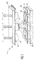
- FIG. 1 schematically represents a known flat screen 1 with microtips 6 comprising a first substrate 2 on which is disposed a cathode 4 provided with microtips 6 electrically controllable by a voltage V cathode (grounded in the example of FIG. 1) and a grid 8 electrically controllable by a voltage V grid and provided with holes 10 at the locations of the microtips 6.
- the first substrate 2 can be made of glass or silicon or any suitable material.
- the flat screen 1 also includes a second substrate 12 facing the first substrate 2 and on which is an anode 14 constituting the emissive surface of the screen 1. Electric conductors 15 transparent or not are disposed on the internal face of the anode 14. Luminophoric materials 17 are deposited on these electrical conductors 15.
- the cathode 4 constitutes the electron source and the anode 14 collects these electrons.
- the emission of electrons by microtips 6 is controlled by the difference of potential applied between the extraction grid 8 and the cathode 4.
- a matrix cathode is produced which has n rows of grid conductors and p columns of cathode conductors driving the microtips.
- the electrical signals applied to these n rows and p columns then allow the display of images of (n * p) points.
- the collection of electrons from microdots 6 is carried out by accelerating them using the "high voltage" applied to the conductors 15 of the anode.
- the light emission is ensured by the phosphor materials 17 under the impact of the electrons received.
- Time color subframes is a method of color control based on a sequential addressing of the anode tracks carrying red, green and blue phosphors. This addressing sequential, is performed at a frequency sufficient high, so the base colors, generated in each of the sub-frames of an image time "melt" together for the eye of the beholder.
- Figure 2 shows a flat screen 1 of art anterior in which the anode 14 is driven by a push-pull circuit 19, arranged outside the screen 1, and using high voltage transistors of switching 18, 20.
- This circuit is connected to the anode emissive 12 by a conductor 22.
- Circuit 19 for driving the transistors 18, 20 includes a source of voltage 24 delivering a voltage Vdd and an opto-coupler 26. The logic control signals, and therefore low voltage of this circuit, are symbolized by inputs v1 and v2.
- control method consists in providing phases of regeneration during which at least part of the conductors of the anode is at low potential and the cathode microtips are polarized in a state resignation. This command mode removes some color drift problems.
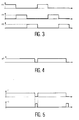
- Figure 3 is a timing diagram showing a example of signal to apply to the anode to generate temporal color subframes.
- Figure 4 is a timing diagram showing a example of signal to apply to the anode to achieve screen regeneration 1.
- Figure 5 a chronogram representing the logic signals v1 and v2 to obtain the anode control voltage in Figure 4.
- the object of the invention is to overcome the disadvantages mentioned above.
- Another object of the invention is to simplify the design of control circuits for flat screens and reduce clutter.
- the power switching component of the electronic circuit for controlling the anode voltage is integrated by construction into the first and second substrates of the screen.
- said power switching component is a high voltage transistor having a first electrode integrated in the first substrate, a second electrode integrated in the second substrate, and a third electrode integrated in the extraction grid.
- the cathode includes conductive columns supporting microtips and the grid has perforated conductive lines crossing said conductive columns to locations of said microtips.
- the anode constitutes the surface emissive of the screen and has at least one surface conductive on which materials are deposited phosphors.
- the electronic circuit of control of the anode voltage is of the push-pull type and further includes a second transistor having a first electrode integrated in the first substrate, a second electrode integrated in the second substrate and electrically connected to the first electrode of the first transistor, and a third control electrode integrated in the grid extraction.
- the transistor equipping the anode voltage control circuit has a first substrate on which are laid a first electrode and a control grid, a second substrate, opposite the first substrate, on which is arranged a second electrode intended to collect the electrons emitted from the first electrode.
- the first electrode constituting the cathode has columns conductive supporting electron sources, the control grid has conductive lines perforated crossing said conductive columns to locations of said electron sources and the second electrode has at least one surface conductive disposed opposite said sources electron.
- the cathode is a source to microdots.
- the cathode is a source to nanotubes.
- the screen according to the invention comprises a module for logic control comprising a low voltage source and an opto-electronic coupler.
- the logic control module has a galvanically isolated charge pump of the screen by a capacitor C.
- FIG. 6 represents a first mode of realization of a microtip flat screen 1 according to the invention comprising a first substrate 2 on which there is a cathode 4 comprising microtips 6 (see Figure 1) arranged in rows and columns.
- An electron extraction grid 8 allows apply sufficient voltage to the microtips 6 to extract electrons from it.
- a second substrate 12 opposite the first substrate 2 supports an anode 14 receiving a high voltage HT intended to accelerate the electrons released by microtips 6.
- the high HV voltage is controlled by a push-pull circuit comprising a first transistor 18 and a second transistor 20 fully integrated in the first substrate 2 and in the second substrate 12 of the screen 1.
- Figure 7 shows a second example of realization of the invention in which the two micropoint transistors 18 and 20 remain unchanged. Only the control logic part 100 is performed at using a charge pump which provides insulation galvanic logic in relation to high voltage through capacity C.
- the transistor 18 has a first electrode 40 integrated in a first zone of the first substrate 2, a second electrode 42 integrated in a second zone of the second substrate 12, and a third electrode 44 integrated into a portion of the extraction grid 8 located between said first and second zones.
- the transistor 20 has a first electrode 50 integrated in a third zone of the first substrate 2, a second electrode 52 integrated in a fourth zone of the second substrate 12, and a third electrode 54 integrated in a second portion of the extraction grid 8 located between the third zone of the first substrate 2 and the fourth zone of the second substrate 12.
- the first electrode 40 of the first transistor 18 is electrically connected to the second electrode 52 of the second transistor 20 by a conductive wire 60. It is possible to choose other technological solutions, to ensure this connection, such as for example a vacuum interconnection at inside the screen 1.
- Figure 8 shows a diagram of the structure transistors 18 and 20 for setting evidence the similarity between the structure of transistors 18, 20 and that of screen 1.
- the transistor 18 (respectively 20) has a first semiconductor substrate 80 on which are arranged the first electrode 40 and a grid of command 44 which is a portion of the grid 8 for extracting screen 1.
- a second semiconductor substrate 86 arranged opposite the first substrate semiconductor 80, supports a second electrode 42 intended to collect the electrons emitted by microtips 6 arranged in rows and columns on the first electrode 40.
- the control grid 44 has perforated conductive lines crossing the conductive columns of the first electrode 40 at the microtip locations 6.
- the semiconductor substrates 80, and 86 respectively form an integral part of substrates 2 and 12 of screen 1.
- the electrodes of transistors 18, 20 are produced in these substrates.
- Figure 9 shows the characteristics current-voltage of a transistor 18, 20.
- microtip transistors differ from conventional MOSFET transistors by their threshold voltages V (gate-cathode) 0 and by the saturation voltage V (anode-cathode) sat which are today a few tens of volts rather than a few volts for conventional MOSFET transistors.
- the voltage withstand of these microtip transistors is limited by the residual vacuum between anode and cathode. We therefore end up with a voltage withstand of the transistors which is that of the screen to be controlled since these transistors are integrated into the very structure of the screen 1.
- the control of the anode 14 of the screen 1 by the transistors with microtips 18, 20, can be achieved by retaining the conventional push-pull circuit.
- microtip transistor of some 10 mm 2 , ie a negligible surface in front of the total surface of the screen.
- the practical realization of microtip transistors is facilitated by the fact that the technological structure of these transistors is simpler than that of a screen. It will be noted that on screen 1, it will be necessary to take implantation precautions to ensure the galvanic isolation of the zones on which the electrodes are integrated.
Landscapes
- Engineering & Computer Science (AREA)
- Physics & Mathematics (AREA)
- Theoretical Computer Science (AREA)
- Chemical & Material Sciences (AREA)
- Nanotechnology (AREA)
- Computer Hardware Design (AREA)
- General Physics & Mathematics (AREA)
- Mathematical Physics (AREA)
- Crystallography & Structural Chemistry (AREA)
- Control Of Indicators Other Than Cathode Ray Tubes (AREA)
- Cathode-Ray Tubes And Fluorescent Screens For Display (AREA)
Abstract
Description
La collection des électrons issus des micropointes 6 est réalisée en les accélérant à l'aide de la "haute tension" appliquée sur les conducteurs 15 de l'anode. L'émission lumineuse est assurée par les matériaux luminophores 17 sous l'impact des électrons reçus.
- des anodes monofil ou multifils pour écrans monochromes ou trichromes décrites dans la publication du CEA dans le document « Recent development on microtips display at LETI. R.MEYER. LETI/CEA ».
- des anodes réflectives pour structure à cathode transparente décrites dans le brevet N° FR 2 633 763 A du CEA.
Selon l'invention, ledit composant de commutation de puissance est un transistor haute tension ayant une première électrode intégrée dans le premier substrat, une deuxième électrode intégrée dans le deuxième substrat, et une troisième électrode intégrée dans la grille d'extraction.
- La figure 1, décrite précédemment, représente schématiquement un écran à micropointe de l'art antérieur ;
- la figure 2, décrite précédemment, représente l'écran plat de la figure 1 relié à un circuit externe de commande de la tension d'anode.
- la figure 3 décrite précédemment représente un chronogramme illustrant une haute tension appliquée à l'anode de l'écran plat de la figure 1 pour générer des sous-trames couleur temporelles ;
- la figure 4 décrite précédemment représente un chronogramme illustrant une haute tension appliquée à l'anode de l'écran de la figure 1 pour régénération d'écran ;
- la figure 5 décrite précédemment représente les signaux logiques de commande des transistors du circuit de la figure 2.
- la figure 6 illustre schématiquement un premier mode de réalisation d'un écran à micropointes selon l'invention ;
- la figure 7 illustre schématiquement un deuxième mode de réalisation d'un écran à micropointes selon l'invention ;
- la figure 8 illustre schématiquement un transistor de commande de la tension d'anode d'un écran selon l'invention ;
- la figure 9 représente les caractéristiques courant-tension d'un transistor à micropointes selon la figure 8 ;
La première électrode 40 du premier transistor 18 est reliée électriquement à la deuxième électrode 52 du deuxième transistor 20 par un fil conducteur 60. Il est possible de choisir d'autres solutions technologiques, pour assurer cette connexion, comme par exemple une interconnexion sous vide à l'intérieur de l'écran 1.
Pour fixer les idées, des spécifications techniques typiques de pilotage d'un écran 1 de 1dm2 sous Va =3 kV sont présentées ci dessous.
Capacité d'anode : Ca = 330 pF.
Temps de commutation anode requis = tc = 100 µs.
Tenir ce temps de commutation nécessite un courant crête de sortie des transistors HT de 10 mA pendant les 100 µs nécessaires à la commutation des anodes. Un tel courant sera facilement délivré par un transistor à micropointes de quelques 10 mm2, soit une surface négligeable devant la surface totale de l'écran.
La réalisation pratique des transistors à micropointes est facilitée par le fait que la structure technologique de ces transistors est plus simple que celle d'un écran.
On notera que sur l'écran 1, il conviendra de prendre des précautions d'implantation pour assurer l'isolement galvanique des zones sur lesquelles sont intégrées les électrodes.
La commutation de la haute tension, est désormais assurée par les transistors à micropointes 18, 20 intégrés à la structure technologique de l'écran 1.
Claims (11)
- Écran plat (1) à émission électronique comportant un premier substrat (2) sur lequel sont disposées une cathode d'émission (4) et une grille d'extraction d'électrons (8), un deuxième substrat (12) en regard du premier substrat (2), sur lequel est disposée une anode (14) destinée à collecter les électrons émis par la cathode (4), et un circuit électronique (19) de commande de la tension d'anode (14) comportant au moins un composant de commutation (18, 20), caractérisé en ce que le composant de commutation (18, 20) est intégré par construction dans le premier substrat (2) et dans le deuxième substrat (12) de l'écran (1).
- Écran selon la revendication 1, caractérisé en ce que ledit composant de commutation (18, 20) est un transistor HT ayant une première électrode (40, 50) intégrée dans le premier substrat (2), une deuxième électrode (42, 52) intégrée dans le deuxième substrat (12), et une troisième électrode (44, 54) intégrée dans la grille d'extraction (8).
- Écran selon la revendication 1, caractérisé en ce que l'anode (14) constitue la surface émissive de l'écran (1) et comporte au moins une surface conductrice (15) sur laquelle sont déposés des matériaux luminophores (17).
- Écran selon la revendication 2, caractérisé en ce que la cathode (4) comporte des colonnes conductrices (32) supportant des sources d'électrons (6), et en ce que la grille (8) comporte des lignes conductrices perforées croisant lesdites colonnes conductrices aux emplacements desdites sources (6).
- Écran selon la revendication 4, caractérisé en ce que la cathode (4) est une source à micropointes.
- Écran selon la revendication 4, caractérisé en ce que la cathode (2) est une source à nanotubes.
- Écran selon l'une des revendications 1 à 6, caractérisé en ce que le circuit électronique (19) est du type push-pull et comporte en outre un deuxième transistor (20) ayant une première électrode (50) intégrée dans le premier substrat (2), une deuxième électrode (52) intégré dans le deuxième substrat (12) et reliée électriquement à la première électrode (50) du premier transistor (18), et une troisième électrode de contrôle (54) intégrée dans la grille d'extraction (8) de l'écran (1).
- Écran selon l'une des revendications 1 à 7, caractérisé en ce qu'il comporte en outre un module de commande logique (100) comportant une source de basse tension Vdd (24) et un coupleur opto-électronique (26).
- Écran selon la revendication 8, caractérisé en ce que le module de commande logique (100) comporte une pompe de charge isolée galvaniquement de l'écran (1) par un condensateur C.
- Transistor, caractérisé en ce qu'il comporte un premier substrat semi-conducteur (80) sur lequel sont disposées une première électrode (40) et une grille de commande (44), un deuxième substrat (86), en regard du premier substrat (80), et sur lequel est disposée une deuxième électrode (42) destinée à collecter les électrons émis par la première électrode (40).
- Transistor selon la revendication 10, caractérisé en ce que la première électrode (40) comporte des micropointes (6) disposées en lignes et en colonnes, la grille de commande (44) comporte des lignes conductrices perforées croisant les colonnes de la première électrode (40) aux emplacements desdites micropointes (6), la deuxième électrode (42) comporte au moins une surface conductrice disposée en regard desdites micropointes (6).
Applications Claiming Priority (2)
| Application Number | Priority Date | Filing Date | Title |
|---|---|---|---|
| FR0103236 | 2001-03-09 | ||
| FR0103236A FR2821982B1 (fr) | 2001-03-09 | 2001-03-09 | Ecran plat a emission electronique et a dispositif integre de commande d'anode |
Publications (1)
| Publication Number | Publication Date |
|---|---|
| EP1239443A1 true EP1239443A1 (fr) | 2002-09-11 |
Family
ID=8860933
Family Applications (1)
| Application Number | Title | Priority Date | Filing Date |
|---|---|---|---|
| EP02290570A Withdrawn EP1239443A1 (fr) | 2001-03-09 | 2002-03-07 | Ercan plat à émission électronique et à dispositif integré de commande d'anode |
Country Status (4)
| Country | Link |
|---|---|
| US (1) | US6876344B2 (fr) |
| EP (1) | EP1239443A1 (fr) |
| JP (1) | JP4307003B2 (fr) |
| FR (1) | FR2821982B1 (fr) |
Citations (5)
| Publication number | Priority date | Publication date | Assignee | Title |
|---|---|---|---|---|
| EP0306173A1 (fr) * | 1987-09-04 | 1989-03-08 | THE GENERAL ELECTRIC COMPANY, p.l.c. | Dispositifs utilisant l'émission de champ |
| EP0362017A1 (fr) * | 1988-09-23 | 1990-04-04 | Thomson-Csf | Composant tel que diode, triode ou dispositif d'affichage cathodoluminescent plat et intégré, et procédé de fabrication |
| EP0747874A1 (fr) * | 1995-06-08 | 1996-12-11 | Pixtech S.A. | Commutation d'une anode d'écran plat de visualisation |
| US5844370A (en) | 1996-09-04 | 1998-12-01 | Micron Technology, Inc. | Matrix addressable display with electrostatic discharge protection |
| US6057636A (en) * | 1996-09-17 | 2000-05-02 | Kabushiki Kaisha Toshiba | Micro power switch using a cold cathode and a driving method thereof |
Family Cites Families (7)
| Publication number | Priority date | Publication date | Assignee | Title |
|---|---|---|---|---|
| FR2568394B1 (fr) * | 1984-07-27 | 1988-02-12 | Commissariat Energie Atomique | Dispositif de visualisation par cathodoluminescence excitee par emission de champ |
| US5225820A (en) | 1988-06-29 | 1993-07-06 | Commissariat A L'energie Atomique | Microtip trichromatic fluorescent screen |
| JP2656843B2 (ja) * | 1990-04-12 | 1997-09-24 | 双葉電子工業株式会社 | 表示装置 |
| JPH06176704A (ja) * | 1992-12-02 | 1994-06-24 | Nippon Hoso Kyokai <Nhk> | 撮像装置及びその動作方法 |
| TW289864B (fr) * | 1994-09-16 | 1996-11-01 | Micron Display Tech Inc | |
| US5689151A (en) * | 1995-08-11 | 1997-11-18 | Texas Instruments Incorporated | Anode plate for flat panel display having integrated getter |
| KR100233254B1 (ko) * | 1996-12-21 | 1999-12-01 | 정선종 | 전계 방출 디스플레이 |
-
2001
- 2001-03-09 FR FR0103236A patent/FR2821982B1/fr not_active Expired - Fee Related
-
2002
- 2002-02-19 US US10/076,454 patent/US6876344B2/en not_active Expired - Fee Related
- 2002-03-07 JP JP2002062620A patent/JP4307003B2/ja not_active Expired - Fee Related
- 2002-03-07 EP EP02290570A patent/EP1239443A1/fr not_active Withdrawn
Patent Citations (5)
| Publication number | Priority date | Publication date | Assignee | Title |
|---|---|---|---|---|
| EP0306173A1 (fr) * | 1987-09-04 | 1989-03-08 | THE GENERAL ELECTRIC COMPANY, p.l.c. | Dispositifs utilisant l'émission de champ |
| EP0362017A1 (fr) * | 1988-09-23 | 1990-04-04 | Thomson-Csf | Composant tel que diode, triode ou dispositif d'affichage cathodoluminescent plat et intégré, et procédé de fabrication |
| EP0747874A1 (fr) * | 1995-06-08 | 1996-12-11 | Pixtech S.A. | Commutation d'une anode d'écran plat de visualisation |
| US5844370A (en) | 1996-09-04 | 1998-12-01 | Micron Technology, Inc. | Matrix addressable display with electrostatic discharge protection |
| US6057636A (en) * | 1996-09-17 | 2000-05-02 | Kabushiki Kaisha Toshiba | Micro power switch using a cold cathode and a driving method thereof |
Also Published As
| Publication number | Publication date |
|---|---|
| FR2821982A1 (fr) | 2002-09-13 |
| JP2002334669A (ja) | 2002-11-22 |
| US20020126072A1 (en) | 2002-09-12 |
| FR2821982B1 (fr) | 2004-05-07 |
| JP4307003B2 (ja) | 2009-08-05 |
| US6876344B2 (en) | 2005-04-05 |
Similar Documents
| Publication | Publication Date | Title |
|---|---|---|
| KR102538996B1 (ko) | 발광 다이오드(led) 테스트 장치 및 제조 방법 | |
| EP0155895B1 (fr) | Procédé d'opération d'écrans de visualisation plats | |
| FR2535498A1 (fr) | Procede et dispositif d'affichage par plasma | |
| FR2604823A1 (fr) | Dispositif emetteur d'electrons et son application notamment a la realisation d'ecrans plats de television | |
| FR2708380A1 (fr) | Dispositif d'affichage d'images et circuit de commande associé. | |
| JPH09503095A (ja) | 表示装置 | |
| US5896115A (en) | Method for driving image display device and unit therefor | |
| EP0383672B1 (fr) | Source lumineuse plane | |
| FR2821982A1 (fr) | Ecran plat a emission electronique et a dispositif integre de commande d'anode | |
| EP0817232B1 (fr) | Procédé de régénération de micropointes d'un écran plat de visualisation | |
| EP0747874A1 (fr) | Commutation d'une anode d'écran plat de visualisation | |
| EP1210721B1 (fr) | Ecran plat a emission de champ avec electrode de modulation | |
| EP0734043A1 (fr) | Ecran plat de visualisation a double grille | |
| US5654729A (en) | Microtip flat panel display with a switched anode | |
| FR2762927A1 (fr) | Anode d'ecran plat de visualisation | |
| EP0625277A1 (fr) | Ecran plat a micropointes protegees individuellement par dipole | |
| Hori et al. | A picture-display panel using a constricted-glow discharge | |
| KR20020030827A (ko) | 전자원, 전자원의 제조방법 및 표시장치 | |
| JP2002110074A (ja) | 電子線励起蛍光体表示装置 | |
| KR100294492B1 (ko) | 평판디스플레이 | |
| EP1147538A1 (fr) | Procede de commande de structure comportant une source d'electrons a effet de champ | |
| KR100456138B1 (ko) | 평면 전계방출 표시소자의 구동장치 및 방법 | |
| FR2809862A1 (fr) | Ecran plat de visualisation a memoire d'adressage | |
| FR2798507A1 (fr) | Dispositif permettant de produire un champ electrique module au niveau d'une electrode et son application aux ecrans plats a emission de champ | |
| Lynch | Development of intensified charge-coupled devices (CCDs) and solid state arrays |
Legal Events
| Date | Code | Title | Description |
|---|---|---|---|
| PUAI | Public reference made under article 153(3) epc to a published international application that has entered the european phase |
Free format text: ORIGINAL CODE: 0009012 |
|
| AK | Designated contracting states |
Kind code of ref document: A1 Designated state(s): AT BE CH CY DE DK ES FI FR GB GR IE IT LI LU MC NL PT SE TR |
|
| AX | Request for extension of the european patent |
Free format text: AL;LT;LV;MK;RO;SI |
|
| 17P | Request for examination filed |
Effective date: 20030208 |
|
| AKX | Designation fees paid |
Designated state(s): DE GB IT |
|
| RAP1 | Party data changed (applicant data changed or rights of an application transferred) |
Owner name: COMMISSARIAT A L'ENERGIE ATOMIQUE |
|
| 17Q | First examination report despatched |
Effective date: 20071122 |
|
| RAP1 | Party data changed (applicant data changed or rights of an application transferred) |
Owner name: COMMISSARIAT A L'ENERGIE ATOMIQUE ET AUX ENERGIES |
|
| STAA | Information on the status of an ep patent application or granted ep patent |
Free format text: STATUS: THE APPLICATION IS DEEMED TO BE WITHDRAWN |
|
| 18D | Application deemed to be withdrawn |
Effective date: 20131001 |