EP0817232B1 - Procédé de régénération de micropointes d'un écran plat de visualisation - Google Patents
Procédé de régénération de micropointes d'un écran plat de visualisation Download PDFInfo
- Publication number
- EP0817232B1 EP0817232B1 EP19970410069 EP97410069A EP0817232B1 EP 0817232 B1 EP0817232 B1 EP 0817232B1 EP 19970410069 EP19970410069 EP 19970410069 EP 97410069 A EP97410069 A EP 97410069A EP 0817232 B1 EP0817232 B1 EP 0817232B1
- Authority
- EP
- European Patent Office
- Prior art keywords
- grid
- regeneration
- cathode
- nominal
- potential
- Prior art date
- Legal status (The legal status is an assumption and is not a legal conclusion. Google has not performed a legal analysis and makes no representation as to the accuracy of the status listed.)
- Expired - Lifetime
Links
Images

Classifications
-
- H—ELECTRICITY
- H01—ELECTRIC ELEMENTS
- H01J—ELECTRIC DISCHARGE TUBES OR DISCHARGE LAMPS
- H01J9/00—Apparatus or processes specially adapted for the manufacture, installation, removal, maintenance of electric discharge tubes, discharge lamps, or parts thereof; Recovery of material from discharge tubes or lamps
- H01J9/02—Manufacture of electrodes or electrode systems
- H01J9/022—Manufacture of electrodes or electrode systems of cold cathodes
- H01J9/025—Manufacture of electrodes or electrode systems of cold cathodes of field emission cathodes
-
- H—ELECTRICITY
- H01—ELECTRIC ELEMENTS
- H01J—ELECTRIC DISCHARGE TUBES OR DISCHARGE LAMPS
- H01J9/00—Apparatus or processes specially adapted for the manufacture, installation, removal, maintenance of electric discharge tubes, discharge lamps, or parts thereof; Recovery of material from discharge tubes or lamps
- H01J9/50—Repairing or regenerating used or defective discharge tubes or lamps
- H01J9/505—Regeneration of cathodes
-
- Y—GENERAL TAGGING OF NEW TECHNOLOGICAL DEVELOPMENTS; GENERAL TAGGING OF CROSS-SECTIONAL TECHNOLOGIES SPANNING OVER SEVERAL SECTIONS OF THE IPC; TECHNICAL SUBJECTS COVERED BY FORMER USPC CROSS-REFERENCE ART COLLECTIONS [XRACs] AND DIGESTS
- Y02—TECHNOLOGIES OR APPLICATIONS FOR MITIGATION OR ADAPTATION AGAINST CLIMATE CHANGE
- Y02W—CLIMATE CHANGE MITIGATION TECHNOLOGIES RELATED TO WASTEWATER TREATMENT OR WASTE MANAGEMENT
- Y02W30/00—Technologies for solid waste management
- Y02W30/50—Reuse, recycling or recovery technologies
- Y02W30/82—Recycling of waste of electrical or electronic equipment [WEEE]
Definitions
- the present invention relates to a flat screen display with microtips.
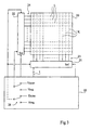
- FIG. 1 represents, partially and in section, the structure of a microtip flat screen of the type to which the invention.
- Such a screen essentially consists of a cathode 1 with microtips 2 and a grid 3 provided with holes 4 at the locations of the microtips 2.
- the cathode 1 is placed in view of a cathodoluminescent anode 5, a substrate of glass 6 constitutes the screen surface.
- the cathode 1 is constituted on a glass substrate 7, cathode conductors 8 organized in columns. These drivers 8 are generally coated with a resistive layer (no represented) of homogenization of the electronic emission.
- the cathode 1 is associated with the gate 3 with the interposition of a layer 9 to isolate the cathode conductors 8 from the grid 3.
- the holes 4 are practiced in the grid layers 3 and isolation 9 to receive the microtips 2 that are formed on the resistive layer.
- Grid 3 is organized in rows, the intersection of a row and a column of the cathode defining a pixel.
- This device uses the electric field created between the cathode 1 and grid 3 so that electrons are extracted micropoints 2 to phosphor elements 10 of the anode 5 through an empty space 11.
- the phosphor elements 10 are deposited on electrodes 12, consisting of a layer transparent conductor such as indium tin oxide (ITO).
- the anode 5 is provided alternating strips of phosphor elements 10 each corresponding to to a color (Red, Green, Blue). Each band is electrically isolated from the two neighboring bands. Groups are arranged parallel to the cathode columns 8, a group three bands (one per color) facing a column cathode. The sets of red, green, blue bands are selectively polarized with respect to the cathode 1, so that the electrons extracted from the microtips 2 a pixel from the cathode / grid are selectively directed to the elements phosphors 10 with respect to each of the colors.
- the anode In the case of a monochrome screen, the anode is usually consisting of a phosphor element plane or two sets of alternating bands of the same color.
- FIG. 2 partially shows an electron emission micropoint cathode associated with an emitted electron extraction grid, to illustrate the addressing of the cathode and the gate during the operation of a microtip screen.
- the anode (5, FIG. 1) and the insulating layer (9, FIG. 1) between the cathode 1 and the gate 3 have not been represented for the sake of clarity.
- only a few microtips 2 have been shown at the intersection of a row L of the grid 3 and a column K of the cathode 1. In practice, these microtips are several thousand per pixel screen .
- the display of an image is carried out during a frame time (for example 20 ms) by properly polarizing the anode, the cathode 1 and the gate 3 by means of an electronic control circuit (not shown).
- a frame time for example 20 ms
- the sets of phosphor strips (10, Fig. 1) are sequentially brought to a potential to attract the electrons. This potential is a function of the distance (empty space 11) separating the cathode / gate from the anode and is, for example, greater than 300 volts.
- the bands 10 are polarized, during a frame, by sets of bands of the same color, or during a subframe duration corresponding to one-third of the frame time (for example 6.6 ms).
- the display is carried out line by line, polarizing sequentially (for example, at 80 volts) the rows L for a duration (for example 30 ⁇ s) corresponding to the duration of a sub-frame divided by the number of rows of the gate 3. While a row L is polarized, the columns K are brought to respective potentials between a maximum transmission potential and a no-emission potential (for example, respectively 0 and 30 volts), to set the brightness of the pixels defined by the intersection of these columns and the row considered.
- the polarization of the columns K changes with each new row L of the line scan.
- the choice of the polarization potential values is related to the characteristics of the phosphor elements 10 and microtips 2. Conventionally, below a potential difference of 50 volts between the cathode 1 and the gate 3 there is no electronic emission, and the maximum emission corresponds to a potential difference of 80 volts.
- Micropoints see their emissive power decrease as and when they are used.
- the screens therefore have a brightness that decreases in time. This decrease is important enough not to be negligible and influences over the life of the screen.
- the present invention aims to propose a method of regeneration microtips according to claim 1 which allows them to give them their original emissive power.
- the present invention also aims to propose a method control of a microtip screen that allows to increase the life of the screen.
- the present invention provides a method of regenerating microtips of a screen viewing plate having a microtip cathode associated with an electron extraction grid, consisting of have the microtips emitted under a current density significantly higher than a nominal current density of operation by applying, between the gate and the cathode, and for a duration significantly greater than a nominal duration addressing in operation, a potential difference significantly higher than nominal differences in potentials of operation.
- the grid is biased to a regeneration potential clearly greater than a nominal operating potential and one polarizes the cathode at a nominal potential corresponding to a transmission Max.
- the display being effected by addressing sequentially the grid rows during said nominal duration and addressing the columns of the cathode individually during the nominal duration of addressing a row, one polarizes at least one grid row at the regeneration potential and all cathode columns at said maximum emission potential during a much longer regeneration time than said nominal duration.
- all the rows of the grid are polarized simultaneously regeneration potential.
- the cathode is biased to a regeneration potential clearly less than a nominal potential corresponding to an emission in operation and the gate is biased to a potential nominal operation.
- Another embodiment also relates to a method of control of a flat display screen comprising a cathode with electron emission microtips, associated with a grid of electron extraction emitted by microtips and anode cathodoluminescent which consists of periodically performing a regeneration cycle.
- the present invention also relates to a flat screen display comprising a microtip cathode, associated to an electron extraction grid and a cathodoluminescent anode, having a first voltage source of polarization of the gate, a second source of voltage of polarization of the grid, and ways to select the first source during normal operation of the screen and the second source during a regeneration cycle of the microtips, the second source delivering a voltage greater than that delivered by the first source.
- a feature of the present invention is provide a particular command of the screen during a cycle of regeneration located outside the display phases. This command consists in forcing the microtips to be emitted under a high current density, increasing the difference in potential between the cathode and the gate, for a time relatively long compared to the classic display time an image frame.
- a regeneration cycle consists in polarizing the rows L of the gate 3 (FIG. 2) at a regeneration potential which is clearly greater than the nominal addressing potential of the rows. While the rows L are brought to the regeneration potential, the cathode 1 is polarized by simultaneously addressing all the columns K to the potential corresponding to the maximum illuminance setpoint when the screen is in operation.
- the increase of the polarization potential of the grid 3 allows to increase the current in each tip 2.
- the current in a peak increases almost a factor of 5 (Fowler and Nordheim Law).
- the bias of the grid to the potential regeneration is preferably effected by means of a signal pulse. Pulse width is significantly higher at the nominal duration of polarization of a row of the grid and the difference between two successive pulses is chosen to leave on the screen the time to cool before the appearance of a new impulse.
- the rows will be polarized, during regeneration, by pulses of the order of 500 ⁇ s with a period of about 10 ms.
- the quantity of electrons passing in a tip during a pulse so the energy dissipated by Joule effect, is thus considerably more important than that which passes in a tip emitting during the operation of the screen.
- the amount of electrons that passes in a point increases by a factor of the order of 80 per compared to an address time of 30 ⁇ s.
- the duration of a regeneration cycle that is, the duration of polarization by the pulse signal depends on the need regeneration. This duration is, for example, between 1 and 10 minutes.
- the method according to the invention is a restoration process which restores the emissive power of the only microtips who need it without affecting others.
- the decrease in brightness due to the loss of power emissive micropoints depends, in fact, their duration of use and may be irregular on the surface of the screen.
- the electrons emitted by the microtips are collected by the grid if the anode of the screen is not addressed. If the anode is addressed, these electrons are then collected by the electrodes of the anode.
- FIG. 3 represents an embodiment of a portion of such a circuit serving to address the cathode and the gate.
- Each column K and each row L of the screen 20 is individually connected to an output of an addressing circuit 21 or 22 associated, respectively, with the cathode 1 or the gate 3.
- An addressing circuit generally comprises as much outputs there rows or columns to address and the outputs of the circuits 21 and 22 are connected by appropriate connectors, respectively 23 and 24, rows L and K columns.
- the circuits 21 and 22 are, for example, constituted by offset registers with parallel outputs.
- the circuits 21 and 22 are controlled by a common block 25 also serving to control the addressing of the anode (not shown).
- the circuit 21 receives from the block 25 the individual polarization instructions I of the columns K and is intended to bias them to the rhythm of the line scan frequency Hsync.
- the circuit 22 is intended to shift the polarization of the gate from one row to the next at the rhythm of the line scan frequency Hsync and receives, from the circuit 25, in addition to the signal Hsync, a nominal bias voltage Vnom (for example , 80 volts).
- Circuits 21 and 22 generally comprise, in addition, entries, respectively Set and Set ', allowing simultaneously force all the outputs to the same level.
- Block 25 has switching means 26 for selecting either the signal Hsync and the potential Vnom, the signal Hreg and the potential Vreg.
- the regeneration of the microtips can also be performed row by row respecting a line scan. Of same, one can perform a regeneration by groups of pixels of the screen by addressing only a certain number of rows and columns.
- An advantage of the present invention is that it allows the implementation of a regeneration of microtips without other intervention that triggering a particular order cycle of the screen.
- the duration of a regeneration cycle (for example, from 1 at 10 minutes) is preferably fixed to be sufficiently long to achieve complete regeneration according to the frequency of regeneration cycles. Note, however, that duration, greater than the time strictly necessary for regeneration complete, is not troublesome to the extent that once that they have regained their original emissive power, the microtips are not affected by regeneration.
- the present invention is capable of various variations and modifications that will appear to the man from art.
- reference has been made in description that precedes an increase in the potential of the grid we can also plan to modify the potential minimum addressing of the cathode columns or both.
- the invention also applies to the case where the illumination instruction of a pixel is fixed by modulation of pulse width of the addressing signals of the columns of the cathode.
Description
Claims (9)
- Procédé de régénération de micropointes (2) d'un écran plat de visualisation comportant une cathode (1) à micropointes (2) associée à une grille (3) d'extraction d'électrons, caractérisé en ce qu'il consiste à faire émettre les micropointes (2) sous une densité de courant nettement supérieure à une densité de courant nominale de fonctionnement en appliquant, entre la grille (3) et la cathode (1), et pendant une durée nettement supérieure à une durée nominale d'adressage en fonctionnement, une différence de potentiels nettement supérieure à des différences nominales de potentiels de fonctionnement.
- Procédé de régénération selon la revendication 1, caractérisé en ce qu'il consiste à polariser la grille (3) à un potentiel de régénération (Vreg) nettement supérieur à un potentiel nominal (Vnom) de fonctionnement et à polariser la cathode (1) à un potentiel nominal correspondant à une émission maximale.
- Procédé de régénération selon la revendication 2, dans lequel la grille (3) est organisée en rangées (L) perpendiculaires à des colonnes (K) de la cathode (1), l'affichage s'effectuant en adressant séquentiellement les rangées de grille (L) pendant ladite durée nominale et en adressant individuellement les colonnes (K) de la cathode pendant la durée nominale d'adressage d'une rangée (L), caractérisé en ce qu'il consiste à polariser au moins une rangée de grille (L) au potentiel de régénération (Vreg) et toutes les colonnes de cathode (K) audit potentiel d'émission maximale pendant une durée de régénération nettement supérieure à ladite durée nominale.
- Procédé de régénération selon la revendication 3, caractérisé en ce qu'il consiste à polariser simultanément toutes les rangées (L) de la grille (3) au potentiel de régénération.
- Procédé de régénération selon la revendication 3 ou 4, caractérisé en ce qu'il consiste à adresser la ou les rangées (L) de la grille (3) au moyen d'un signal (Hreg) comprenant des impulsions d'une durée nettement supérieure à ladite durée nominale, l'écart entre deux impulsions successives étant nettement supérieur à la durée d'une impulsion.
- Procédé de régénération selon la revendication 1, caractérisé en ce qu'il consiste à polariser la cathode (1) à un potentiel de régénération nettement inférieur à un potentiel nominal correspondant à une émission maximale en fonctionnement et à polariser la grille (3) à un potentiel nominal de fonctionnement (Vnom).
- Procédé de commande d'un écran plat de visualisation comportant une cathode (1) à micropointes (2) d'émission électronique, associée à une grille (3) d'extraction d'électrons émis par les micropointes (2) et à une anode (5) cathodoluminescente, caractérisé en ce qu'il consiste à mettre en oeuvre le procédé de régénération selon l'une quelconque des revendications 1 à 6.
- Procédé de commande selon la revendication 7, caractérisé en ce qu'il consiste à effectuer périodiquement un cycle de régénération.
- Écran plat de visualisation comportant une cathode (1) à micropointes (2), associée à une grille (3) d'extraction d'électrons et à une anode (5) cathodoluminescente, caractérisé en ce qu'il comporte :une première source de tension de polarisation (Vnom) de la grille (3) ;une deuxième source de tension de polarisation (Vreg) de la grille (3) ; etdes moyens (26) pour sélectionner la première source pendant un fonctionnement normal de l'écran et la deuxième source pendant un cycle de régénération des micropointes (2), la deuxième source délivrant une tension supérieure à celle délivrée par la première source.
Applications Claiming Priority (2)
| Application Number | Priority Date | Filing Date | Title |
|---|---|---|---|
| FR9608487 | 1996-07-02 | ||
| FR9608487A FR2750785B1 (fr) | 1996-07-02 | 1996-07-02 | Procede de regeneration de micropointes d'un ecran plat de visualisation |
Publications (2)
| Publication Number | Publication Date |
|---|---|
| EP0817232A1 EP0817232A1 (fr) | 1998-01-07 |
| EP0817232B1 true EP0817232B1 (fr) | 2005-10-12 |
Family
ID=9493815
Family Applications (1)
| Application Number | Title | Priority Date | Filing Date |
|---|---|---|---|
| EP19970410069 Expired - Lifetime EP0817232B1 (fr) | 1996-07-02 | 1997-07-01 | Procédé de régénération de micropointes d'un écran plat de visualisation |
Country Status (5)
| Country | Link |
|---|---|
| US (1) | US6081247A (fr) |
| EP (1) | EP0817232B1 (fr) |
| JP (1) | JP3978816B2 (fr) |
| DE (1) | DE69734337T2 (fr) |
| FR (1) | FR2750785B1 (fr) |
Families Citing this family (6)
| Publication number | Priority date | Publication date | Assignee | Title |
|---|---|---|---|---|
| US6259422B1 (en) * | 1997-08-06 | 2001-07-10 | Canon Kabushiki Kaisha | Method for producing image-forming apparatus |
| US6104139A (en) * | 1998-08-31 | 2000-08-15 | Candescent Technologies Corporation | Procedures and apparatus for turning-on and turning-off elements within a field emission display device |
| FR2792771B1 (fr) * | 1999-04-22 | 2001-07-27 | Cit Alcatel | Generateur impulsionnel d'electrons |
| FR2800510B1 (fr) * | 1999-10-28 | 2001-11-23 | Commissariat Energie Atomique | Procede de commande de structure comportant une source d'electrons a effet de champ |
| US7145527B2 (en) * | 2001-06-29 | 2006-12-05 | Lg Electronics Inc. | Field emission display device and driving method thereof |
| US6988921B2 (en) * | 2002-07-23 | 2006-01-24 | Canon Kabushiki Kaisha | Recycling method and manufacturing method for an image display apparatus |
Family Cites Families (6)
| Publication number | Priority date | Publication date | Assignee | Title |
|---|---|---|---|---|
| FR2098954A5 (fr) * | 1970-07-31 | 1972-03-10 | Anvar | |
| US3817592A (en) * | 1972-09-29 | 1974-06-18 | Linfield Res Inst | Method for reproducibly fabricating and using stable thermal-field emission cathodes |
| US4818914A (en) * | 1987-07-17 | 1989-04-04 | Sri International | High efficiency lamp |
| EP0729171B1 (fr) * | 1990-12-28 | 2000-08-23 | Sony Corporation | Procédé de fabrication d'un dispositif d'affichage plat |
| US5262698A (en) * | 1991-10-31 | 1993-11-16 | Raytheon Company | Compensation for field emission display irregularities |
| US5554828A (en) * | 1995-01-03 | 1996-09-10 | Texas Instruments Inc. | Integration of pen-based capability into a field emission device system |
-
1996
- 1996-07-02 FR FR9608487A patent/FR2750785B1/fr not_active Expired - Fee Related
-
1997
- 1997-06-26 US US08/883,051 patent/US6081247A/en not_active Expired - Fee Related
- 1997-07-01 EP EP19970410069 patent/EP0817232B1/fr not_active Expired - Lifetime
- 1997-07-01 DE DE1997634337 patent/DE69734337T2/de not_active Expired - Fee Related
- 1997-07-02 JP JP19073797A patent/JP3978816B2/ja not_active Expired - Lifetime
Also Published As
| Publication number | Publication date |
|---|---|
| DE69734337T2 (de) | 2006-07-13 |
| FR2750785A1 (fr) | 1998-01-09 |
| JP3978816B2 (ja) | 2007-09-19 |
| JPH10275579A (ja) | 1998-10-13 |
| US6081247A (en) | 2000-06-27 |
| FR2750785B1 (fr) | 1998-11-06 |
| DE69734337D1 (de) | 2006-02-23 |
| EP0817232A1 (fr) | 1998-01-07 |
Similar Documents
| Publication | Publication Date | Title |
|---|---|---|
| EP0704877B1 (fr) | Protection électrique d'une anode d'écran plat de visualisation | |
| EP0349425B1 (fr) | Ecran fluorescent trichrome à micropointes | |
| FR2709375A1 (fr) | Dispositif d'affichage d'images et circuit de commande associé. | |
| EP0155895A1 (fr) | Procédé d'opération d'écrans de visualisation plats | |
| EP0349426B1 (fr) | Ecran fluorescent à micropointes ayant un nombre réduit de circuits d'adressage et procédé d'adressage de cet écran | |
| EP0817232B1 (fr) | Procédé de régénération de micropointes d'un écran plat de visualisation | |
| EP0893817B1 (fr) | Pompage ionique d'un écran plat à micropointes | |
| EP0734042B1 (fr) | Anode d'écran plat de visualisation à bandes résistives | |
| EP0292376B1 (fr) | Dispositif d'affichage électroluminescent à effet mémoire et à demi-teintes | |
| EP0734043B1 (fr) | Ecran plat de visualisation a double grille | |
| EP0747875B1 (fr) | Procédé de commande d'écran plat de visualisation | |
| FR2735265A1 (fr) | Commutation d'une anode d'ecran plat de visualisation | |
| EP0649162A1 (fr) | Ecran plat à micropointes à anode commutée | |
| EP1147538B1 (fr) | Procede de commande de structure comportant une source d'electrons a effet de champ | |
| EP0337833A1 (fr) | Procédé de commande point par point d'un panneau à plasma | |
| EP1005012B1 (fr) | Adressage numérique d'un écran plat de visualisation | |
| EP0844642A1 (fr) | Ecran plat de visualisation à grilles focalisatrices | |
| FR2762927A1 (fr) | Anode d'ecran plat de visualisation | |
| EP0905670A1 (fr) | Simplification de l'adressage d'un écran à micropointes avec électrode de rappel | |
| EP0867908A1 (fr) | Uniformisation de l'émission électronique potentielle d'une cathode d'écran plat à micropointes | |
| FR2790861A1 (fr) | Dispositif d'attaque pour dispositif luminescent a emission par effet de champ | |
| EP1120772A1 (fr) | Régénération d'anodes d'écran plat de visualisation | |
| FR2809862A1 (fr) | Ecran plat de visualisation a memoire d'adressage | |
| FR2760283A1 (fr) | Procede et dispositif de reglage des coordonnees chromatiques d'un ecran plat de visualisation | |
| EP1073088A1 (fr) | Procédé de fabrication d'une anode d'un écran plat de visualisation, anode obtenue par ce procédé et écran plat utilisant cette anode |
Legal Events
| Date | Code | Title | Description |
|---|---|---|---|
| PUAI | Public reference made under article 153(3) epc to a published international application that has entered the european phase |
Free format text: ORIGINAL CODE: 0009012 |
|
| AK | Designated contracting states |
Kind code of ref document: A1 Designated state(s): DE FR GB IT |
|
| 17P | Request for examination filed |
Effective date: 19980613 |
|
| AKX | Designation fees paid |
Free format text: DE FR GB IT |
|
| RBV | Designated contracting states (corrected) |
Designated state(s): DE FR GB IT |
|
| 111Z | Information provided on other rights and legal means of execution |
Free format text: DE FR GB IT |
|
| 17Q | First examination report despatched |
Effective date: 20020205 |
|
| GRAH | Despatch of communication of intention to grant a patent |
Free format text: ORIGINAL CODE: EPIDOS IGRA |
|
| GRAH | Despatch of communication of intention to grant a patent |
Free format text: ORIGINAL CODE: EPIDOS IGRA |
|
| 19U | Interruption of proceedings before grant |
Effective date: 20020621 |
|
| 19W | Proceedings resumed before grant after interruption of proceedings |
Effective date: 20050502 |
|
| RAP1 | Party data changed (applicant data changed or rights of an application transferred) |
Owner name: LE COMMISSARIAT AE L'ENERGIE ATOMIQUE |
|
| GRAA | (expected) grant |
Free format text: ORIGINAL CODE: 0009210 |
|
| AK | Designated contracting states |
Kind code of ref document: B1 Designated state(s): DE FR GB IT |
|
| REG | Reference to a national code |
Ref country code: GB Ref legal event code: FG4D Free format text: NOT ENGLISH |
|
| GBT | Gb: translation of ep patent filed (gb section 77(6)(a)/1977) |
Effective date: 20060116 |
|
| REF | Corresponds to: |
Ref document number: 69734337 Country of ref document: DE Date of ref document: 20060223 Kind code of ref document: P |
|
| PLBE | No opposition filed within time limit |
Free format text: ORIGINAL CODE: 0009261 |
|
| STAA | Information on the status of an ep patent application or granted ep patent |
Free format text: STATUS: NO OPPOSITION FILED WITHIN TIME LIMIT |
|
| 26N | No opposition filed |
Effective date: 20060713 |
|
| PGFP | Annual fee paid to national office [announced via postgrant information from national office to epo] |
Ref country code: DE Payment date: 20070731 Year of fee payment: 11 |
|
| PGFP | Annual fee paid to national office [announced via postgrant information from national office to epo] |
Ref country code: GB Payment date: 20070621 Year of fee payment: 11 |
|
| PGFP | Annual fee paid to national office [announced via postgrant information from national office to epo] |
Ref country code: IT Payment date: 20070711 Year of fee payment: 11 |
|
| PGFP | Annual fee paid to national office [announced via postgrant information from national office to epo] |
Ref country code: FR Payment date: 20070724 Year of fee payment: 11 |
|
| GBPC | Gb: european patent ceased through non-payment of renewal fee |
Effective date: 20080701 |
|
| PG25 | Lapsed in a contracting state [announced via postgrant information from national office to epo] |
Ref country code: DE Free format text: LAPSE BECAUSE OF NON-PAYMENT OF DUE FEES Effective date: 20090203 |
|
| REG | Reference to a national code |
Ref country code: FR Ref legal event code: ST Effective date: 20090331 |
|
| PG25 | Lapsed in a contracting state [announced via postgrant information from national office to epo] |
Ref country code: GB Free format text: LAPSE BECAUSE OF NON-PAYMENT OF DUE FEES Effective date: 20080701 |
|
| PG25 | Lapsed in a contracting state [announced via postgrant information from national office to epo] |
Ref country code: IT Free format text: LAPSE BECAUSE OF NON-PAYMENT OF DUE FEES Effective date: 20080701 Ref country code: FR Free format text: LAPSE BECAUSE OF NON-PAYMENT OF DUE FEES Effective date: 20080731 |