EP1237210A1 - Method for producing electrode for lithium secondary cell - Google Patents
Method for producing electrode for lithium secondary cell Download PDFInfo
- Publication number
- EP1237210A1 EP1237210A1 EP00969920A EP00969920A EP1237210A1 EP 1237210 A1 EP1237210 A1 EP 1237210A1 EP 00969920 A EP00969920 A EP 00969920A EP 00969920 A EP00969920 A EP 00969920A EP 1237210 A1 EP1237210 A1 EP 1237210A1
- Authority
- EP
- European Patent Office
- Prior art keywords
- thin film
- active material
- current collector
- electrode
- fabricating
- Prior art date
- Legal status (The legal status is an assumption and is not a legal conclusion. Google has not performed a legal analysis and makes no representation as to the accuracy of the status listed.)
- Withdrawn
Links
Images


Classifications
-
- H—ELECTRICITY
- H01—ELECTRIC ELEMENTS
- H01M—PROCESSES OR MEANS, e.g. BATTERIES, FOR THE DIRECT CONVERSION OF CHEMICAL ENERGY INTO ELECTRICAL ENERGY
- H01M4/00—Electrodes
- H01M4/02—Electrodes composed of, or comprising, active material
- H01M4/13—Electrodes for accumulators with non-aqueous electrolyte, e.g. for lithium-accumulators; Processes of manufacture thereof
- H01M4/139—Processes of manufacture
- H01M4/1395—Processes of manufacture of electrodes based on metals, Si or alloys
-
- H—ELECTRICITY
- H01—ELECTRIC ELEMENTS
- H01M—PROCESSES OR MEANS, e.g. BATTERIES, FOR THE DIRECT CONVERSION OF CHEMICAL ENERGY INTO ELECTRICAL ENERGY
- H01M10/00—Secondary cells; Manufacture thereof
- H01M10/05—Accumulators with non-aqueous electrolyte
- H01M10/052—Li-accumulators
- H01M10/0525—Rocking-chair batteries, i.e. batteries with lithium insertion or intercalation in both electrodes; Lithium-ion batteries
-
- H—ELECTRICITY
- H01—ELECTRIC ELEMENTS
- H01M—PROCESSES OR MEANS, e.g. BATTERIES, FOR THE DIRECT CONVERSION OF CHEMICAL ENERGY INTO ELECTRICAL ENERGY
- H01M4/00—Electrodes
- H01M4/02—Electrodes composed of, or comprising, active material
- H01M4/04—Processes of manufacture in general
- H01M4/0402—Methods of deposition of the material
- H01M4/0404—Methods of deposition of the material by coating on electrode collectors
-
- H—ELECTRICITY
- H01—ELECTRIC ELEMENTS
- H01M—PROCESSES OR MEANS, e.g. BATTERIES, FOR THE DIRECT CONVERSION OF CHEMICAL ENERGY INTO ELECTRICAL ENERGY
- H01M4/00—Electrodes
- H01M4/02—Electrodes composed of, or comprising, active material
- H01M4/04—Processes of manufacture in general
- H01M4/0402—Methods of deposition of the material
- H01M4/0421—Methods of deposition of the material involving vapour deposition
- H01M4/0423—Physical vapour deposition
- H01M4/0426—Sputtering
-
- H—ELECTRICITY
- H01—ELECTRIC ELEMENTS
- H01M—PROCESSES OR MEANS, e.g. BATTERIES, FOR THE DIRECT CONVERSION OF CHEMICAL ENERGY INTO ELECTRICAL ENERGY
- H01M4/00—Electrodes
- H01M4/02—Electrodes composed of, or comprising, active material
- H01M4/36—Selection of substances as active materials, active masses, active liquids
- H01M4/38—Selection of substances as active materials, active masses, active liquids of elements or alloys
-
- Y—GENERAL TAGGING OF NEW TECHNOLOGICAL DEVELOPMENTS; GENERAL TAGGING OF CROSS-SECTIONAL TECHNOLOGIES SPANNING OVER SEVERAL SECTIONS OF THE IPC; TECHNICAL SUBJECTS COVERED BY FORMER USPC CROSS-REFERENCE ART COLLECTIONS [XRACs] AND DIGESTS
- Y02—TECHNOLOGIES OR APPLICATIONS FOR MITIGATION OR ADAPTATION AGAINST CLIMATE CHANGE
- Y02E—REDUCTION OF GREENHOUSE GAS [GHG] EMISSIONS, RELATED TO ENERGY GENERATION, TRANSMISSION OR DISTRIBUTION
- Y02E60/00—Enabling technologies; Technologies with a potential or indirect contribution to GHG emissions mitigation
- Y02E60/10—Energy storage using batteries
-
- Y—GENERAL TAGGING OF NEW TECHNOLOGICAL DEVELOPMENTS; GENERAL TAGGING OF CROSS-SECTIONAL TECHNOLOGIES SPANNING OVER SEVERAL SECTIONS OF THE IPC; TECHNICAL SUBJECTS COVERED BY FORMER USPC CROSS-REFERENCE ART COLLECTIONS [XRACs] AND DIGESTS
- Y10—TECHNICAL SUBJECTS COVERED BY FORMER USPC
- Y10T—TECHNICAL SUBJECTS COVERED BY FORMER US CLASSIFICATION
- Y10T29/00—Metal working
- Y10T29/49—Method of mechanical manufacture
- Y10T29/49002—Electrical device making
Definitions
- the present invention relates to a method for fabricating a novel electrode for a rechargeable lithium battery.
- Rechargeable lithium batteries are reported (Solid State Ionics, 113-115, p57 (1998)) which use an electrode consisting of aluminum, silicon, tin or the like that is electrochemically alloyed with lithium on charge.
- a silicon electrode provides a particularly high theoretical capacity and is promising as a high-capacity.
- various rechargeable batteries using silicon for the negative electrode are proposed (Japanese Patent Laid-Open No. Hei 10-255768).
- alloying negative electrodes fail to provide sufficient cycle characteristics since alloys, as electrode active materials, are themselves pulverized on charge and discharge to reduce current-collecting capabilities.
- the present applicant has proposed a rechargeable lithium battery which incorporates a microcrystalline or amorphous silicon thin film deposited on a current collector by a CVD, sputtering or other thin-film forming processes (Japanese Patent Laying-Open No. Hei 11-301646 and others).
- a method for fabricating an electrode for a rechargeable lithium battery includes depositing a thin film composed of active material capable of alloy formation with lithium on a current collector made of a metal incapable of alloy formation with lithium, using a process for depositing a thin film by supplying a material thereof from a gas phase, and is characterized in that the thin film of active material is deposited at such a temperature that enables formation of a mixed layer via diffusion of a constituent of the current collector into the thin film in.the vicinity of an interface therebetween.
- Examples of processes that can deposit a thin film of active material by supplying the material from a gas phase include sputtering, CVD, vacuume evaporation and spraying processes.
- any material can be used for the active material if it can form an alloy with lithium.
- examples of such materials include silicon, germanium, tin, lead, zinc, magnesium, sodium, aluminum, gallium, indium and the like.
- the active material composed mainly of silicon or germanium is preferred.
- the active material composed mainly of silicon is particularly preferred.
- the thin film of active material has the amorphous or microcrystalline form. Accordingly, an amorphous or microcrystalline silicon thin film is preferred as the thin film of active material.
- the thin film is identified as an amorphous silicon thin film when Raman spectroscopy detects the substantial absence of a peak around 520 cm -1 corresponding to a crystal region, and as a microcrystalline thin film when Raman spectroscopy detects the substantial presence of a peak around 520 cm -1 corresponding to a crystalline region and a peak around 480 cm -1 corresponding to an amorphous region.
- Other examples of preferred thin films include an amorphous germanium thin film, a microcrystalline germanium thin film, an amorphous silicon-germanium alloy thin film, and a microcrystalline silicon-germanium alloy thin film.
- the current collector for use in the present invention is composed of a material incapable of alloy formation with lithium, such as copper.
- the thin film of active material is deposited at such a temperature that enables formation of a mixed layer via diffusion of a constituent of the current collector into the thin film in the vicinity of an interface therebetween. That is, the diffusion of the current collector constituent into the thin film of active material is promoted as the temperature (thin-film forming temperature) at which the thin film of active material is deposited is increased. Accordingly, in the present invention, the thin film of active material is deposited at a temperature that enables sufficient diffusion of the current collector constituent into the thin film and sufficient formation, in the thin film, of the mixed layer 'consisting of the current collector constituent and the active material.
- the formation of the mixed layer via diffusion of the current collector constituent into the thin film of active material improves adhesion of the thin film to the current collector.
- the current collector constituent is a metal element which does not form an alloy with lithium.
- the diffusion of such a current collector constituent into the thin film of active material results in the relative reduction of expansion and shrinkage of the thin film of active material when it stores and releases lithium.
- a stress produced in the thin film of active material when it expands and shrinks is thus lowered in its location adjacent to the current collector. This prevents the thin film of active material, if its volume expands and shrinks, from separating from the current collector, and thus achieves further improvement of adhesion between the current collector and the thin film of active material.
- the concentration of the current collector constituent in the thin film is found to be higher in the vicinity of an interface between the thin film and the current collector, and is lower at a location closer to the surface of the thin film of active material.
- This continuously decreasing concentration gradient of the current collector constituent in the mixed layer is considered to indicate the formation of a solid solution between the current collector constituent and the active material.
- the higher thin film-forming temperature causes the excessive diffusion of the current collector constituent into the thin film and results in the increased tendency of the current collector constituent to form an intermetallic compound with the active material.
- the formation of such an intermetallic compound reduces the number of sites serving as the active material since the active material atoms are incorporated in the compound, so that a charge-discharge capacity of the thin film of active material is reduced.
- the formation of the intermetallic compound also reduces adhesion of the current collector to the thin film of active material. It is thus preferred that the thin film of active material is deposited on the current collector at such a temperature that does not produce, in the mixed layer, an intermetallic compound between the active material and the current collector constituent. Such a temperature is preferably below 300 °C.
- a heat treatment may be performed after the thin film of active material is deposited on the current collector.
- the heat treatment allows further diffusion of the current collector constituent into the thin film.
- the heat treatment is carried out under the conditions that avoid excessive diffusion of the current collector constituent and thus prevent formation of an intermetallic compound between the current collector constituent and the active material, as described above.
- a temperature for the heat treatment is preferably below 650 °C, more preferably 400 °C or lower.
- the particularly preferred current collector constituent that diffuses into the thin film is copper.
- at least a surface portion of the current collector is composed mainly of copper, since the copper diffuses from the surface portion of the current collector into the thin film.
- the thin film of active material can be deposited by sputtering.
- a power density applied to a target containing constituent atoms of the active material is preferably 50 W/cm 2 or lower, more preferably 6 W/cm 2 or lower.
- the power may be supplied in any form, such as a DC, RF or pulse voltage.
- the deposition of the thin film of active material is preferably effected in an intermittent fashion.
- the intermittent deposition of the thin film of active material is effective to lower a deposition temperature, i.e., a maximum temperature attained during deposition of the thin film. This therefore enables deposition of the active material under the conditions that the intermetallic compound is hardly produced.
- One method of achieving intermittent deposition of the active material on the current collector is to place the current collector on an outer periphery of a drum-like holder and deposit the thin film of active material on the current collector while rotating the holder.
- the above-described process for depositing the thin film by supplying a material thereof from a gas phase is preferably practiced under the following conditions.
- a substrate temperature is preferably below 300 °C, as described above. If the substrate temperature is excessively high, an intermetallic compound between the active material and the current collector constituent is occasionally formed.
- the deposition rate is preferably 0.01 nm/sec (0.1 ⁇ /sec) or above. If the deposition rate is excessively low, the influence of surface diffusion and rearrangement becomes significant, even at low temperatures, to bring the process close to a thermal equilibrium, resulting in the increased tendency to form the intermetallic compound.
- a pressure (degree of vacuum) of the atmosphere is preferably in the approximate range of 10 -2 - 10 2 Pa. If this atomospheric pressure (degree of vacuum) goes beyond the specified range, it becomes more likely that a thin film is provided as if formed by deposition of powder particles to result in the reduced adhesion thereof to the current collector. On the other hand, if the atomospheric pressure (degree of vacuum) falls below the specified range, the deposition rate becomes extremely slow to result in the increased tendency to produce the intermetallic compound, as described above.
- a power density applied to a target is preferably 50 W/cm 2 or less, more preferably 6 W/cm 2 or less. If the power density applied to the target is increased excessively, the influence of a radiation heat from a plasma becomes significant to result in the increased tendency of the active material to form the intermetallic compound.
- the preferred sputtering gas is a gas which does not react with a target material such as silicon. From such a point of view, inert gases are preferred including He, Ne, Ar, Kr, Xe, Rn and the like. Among these gases, an Ar gas is particularly preferred for its ability to readily produce a plasma and provide a high sputtering efficiency.
- a target for use in sputtering preferably has a single crystal or polycrystalline structure. Also preferably, its purity is at least 99 %. These are to minimize inclusion of impurities in the resulting thin film of active material.
- an interior of a chamber before the start of thin-film deposition is maintained at a pressure of not exceeding 0.1 Pa. This is also effective to minimize inclusion of impurities in the resulting thin film of active material.
- the current collector as the substrate is preferably subjected to a pretreatment, such as plasma irradiation.
- This plasma irradiation may be in the form of Ar or hydrogen plasma irradiation.
- the current collector can be cleaned at its surface by such a pretreatment.
- this pretreatment causes a temperature rise of the substrate. It is accordingly preferred that the substrate temperature is controlled to stay below 300 °C.
- the current collector as the substrate may preferably be subjected to cleaning before the deposition of the thin film to clean the surface of the current collector.
- useful cleaning agents include water, organic solvents, acids, alkalines, neutral detergents and combinations thereof.
- the heat treatment is preferably effected at a temperature of 650 °C or lower, more preferably 400 °C or lower.
- the intermetallic compound may be produced, as described earlier.
- the thin film of active material is deposited onto the current collector in an intermittent manner.
- the current collector is placed on an outer periphery of a drum-like holder and the thin film is deposited on the current collector while rotating the holder, or the current collector is placed on a reciprocating holder and the thin film is intermittently deposited on the current collector.
- a possible alternative is to arrange plural targets and allow the current collector to pass through regions opposing the respective targets in a sequential manner so as to deposit the thin film intermittently.
- Such intermittent deposition of the thin film of active material suppresses a temperature rise of the substrate.
- the thickness of the thin film deposited each time in the intermittent deposition is preferably 1 ⁇ m or less.
- a rolled copper foil (about 26 ⁇ m thick) was roughend at its surface via copper deposition by an electrolytic process to provide a current collector.
- a silicon thin film was formed on the current collector using a parallel-plate.
- RF sputtering apparatus An Ar gas alone was used as a sputtering gas. 99.999 % pure, single crystal silicon was used as a target.
- the negative electrodes of Examples 1 - 7 and Comparative Examples 1 - 3 were fabricated under the thin-film forming conditions as specified in Tables 1 and 2, while adjusting a flow rate of the Ar gas or an opening degree of an exhaust valve.
- the silicon thin film was formed to a thickness of about 6 ⁇ m.
- Example 1 - 3 and Comparative Examples 1 - 2 the substrate temperature was varied to form silicon thin films (thin films of active material) at different thin-film forming temperatures (maximum attainable temperatures).
- Example 4 and Comparative Example 3 the deposited thin films were further subjected to a heat treatment under the conditions specified in Table 2.
- the power density applied to the target was varied to form thin films.
- the crystallinities of the resulting silicon thin films were identified by Raman spectroscopy.
- the silicon thin film was identified as. being "amorphous" when the substantial presence of a peak around 480 cm -1 and the substantial absence of a peak around 520 cm -1 were observed and as being “polycrystalline” when the substantial absence of a peak around 480 cm -1 and the substantial presence of a sigle peak around 520 cm -1 were observed.
- Each silicon thin film was deposited on a limited, 2.5 cm x 2.5 cm surface region of the copper foil by using a mask. After deposition of the silicon thin film, a negative electrode tab was attached onto a surface portion of the copper foil that was left uncoated with the silicon thin film to complete a negative electrode.
- LiPF 6 1 mole/liter was dissolved in a mixed solvent containing equi-volumes of ethylene carbonate and dimethyl carbonate to prepare an electrolyte solution for use in the following battery construction.
- FIG 2 is a perspective view of such constructed rechargeable lithium battery.
- Figure 3 is a schematic sectional view of the constructed rechargeable lithium battery.
- the positive electrode and the negative electrode are inserted into an interior of a casing 10.
- a layer of negative active material in the form of a silicon thin film 12 is provided on a negative current collector 11.
- a layer 14 of positive active material is provided on a positive current collector 13.
- a separator 15 is interposed between the silicon thin film 12 and the layer 14 of positive active material.
- the electrolyte solution is introduced into the casing 10.
- the casing 10 is welded at its ends to.define a sealed portion 10a.
- the negative electrode tab 17 attached to the negative current collector 11 extends thourgh the sealed portion 10a to an outside.
- the positive electrode tab 18 attached to the positive current collector 13 also extends thourgh the sealed portion 10a to an outside.
- the rechargeable lithium batteries constructed in the manner as described above were subjected to a charge-discharge cycle test. Each battery was charged at a current of 9 mA to a charge end capacity of 9 mAh and then discharged at a current of 9 mA to a discharge end voltage of 2.75 V. This unit charge-discharge cycle was repeated to measure 1st-cycle, 5th-cycle and 20th-cycle discharge capacities and charge-discharge efficiencies. The results. are shown in Tables 1 and 2.
- the unit of flow rate, sccm indicates a volumetric flow rate per minute (cm 3 /minute) of a fluid at 0 °C at 1 atmospheric pressure (101.33 kPa) and is an abbreviation of standard cubic centimeters per minute.
- the silicon thin film is rendered into a polycrystalline form and the discharge capacity and charge-discharge efficiency drop when the deposition of the thin film was followed by heat treatment at a temperature of 650 °C.
- a temperature for the heat treatment is preferably below 650 °C, more preferably 400 °C or lower.
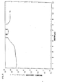
- the negative electrodes fabricated in Examples 1 - 3 and Comparative Examples 1 - 2 by varying the substrate temperature so as to vary the thin-film forming temperature (maximum attainable temperature) were measured for a concentration distribution of a copper element in a depth direction by SIMS (secondary ion mass spectrometry). Each negative electrode before subjected to a charge-discharge test was measured .for a concentration distribution of a copper element ( 63 Cu + ) using O 2 + as a sputtering source.
- Figures 4 - 8 illustrate concentration distributions of copper along depths of the negative electrodes fabricated in Examples 1 -3 and Comparative Examples 1 - 2. Each abscissa indicates a depth ( ⁇ m) and each ordinate indicates an atomic density (atoms/cc : atoms/cm 3 ). Figure 4 corrsponds to Example 1, Figure 5 to Example 2, Figure 6 to Example 3, Figure 7 to Comparative Example 1, and Figure 8 to Comparative Example 2.
- the thin film has a thickness region, in the vicinity of its top surface, where the copper concentration shows no substantial change and is relatively low.
- the thin film also has a thickness region where the copper concentration increases from the top surface of the thin film toward an interface between the thin film and the current collector.
- the presence of such a thickness region with an increaseing copper concentration clearly indicates the existence of a mixed layer consisting of the active material and the copper element in the thin film adjacent the interface between the thin film and the current collector.
- the existence of such a mixed region (mixed layer) is believed to result in a marked improvement in adhesion between the current collector and the thin film.
- the silicon thin film was deposited onto a current collector similar in type to that used in Experiment 1.
- the current collector was placed on an outer periphery of the rotating holder 1 shown in Figure 1. While the rotating holder 1 was rotated, a radio-frequency (RF) power from an RF power supply 3 was supplied to the target 2 to generate an Ar plasma 4, so that the silicon thin film was deposited on the current collector.
- the rotating holder 1 was rotated at a speed of about 10 rpm.
- Other thin-film forming conditions are specified in Table 3.
- An Ar gas alone was used for the sputtering gas.
- the target used was similar in type to that specified in Experiment 1.
- the silicon thin film was deposited to a thickness of about 6 ⁇ m.
- Example 8 the deposition temperature (maximum attainable temperature) in Example 8 is lower than in Example 1, although the power density applied to the target in Example 8 is slightly higher than in Example 1 and the remaining forming conditions are identical.
- the current collector is placed on a rotating holder and the active material is deposited thereon while the rotating holder is rotated so that the deposition of silicon on the current collector is achieved in an intermittent manner. This is believed to successfully hold the maximum attainable temperature down at a lower level. It is also appreciated that slightly better discharge capacity and charge-discharge efficiency are obtained in Example 8 than in Example 1.
- Example 1 of Experiment 1 The same parallel-plate sputtering apparatus as in Experiment 1 was used. The procedure of Example 1 of Experiment 1 was followed, except that a DC or pulse power, instead of the radio-frequency (RF) power, was applied to the target at the power density specified in Table 4, to deposit a silicon thin film on a current collector and fabricate a negative electrode.
- RF radio-frequency
- the thin films of active material are formed by a sputtering technique in the preceding Examples, the present invention is not limited thereto.
- the CVD or other thin-film forming processes can also be used.
- an electrode for a rechargeable lithium battery can be stably fabricated which exhibits a high charge-discharge capacity and superior charge-discharge cycle characteristics.
Landscapes
- Chemical & Material Sciences (AREA)
- Engineering & Computer Science (AREA)
- Chemical Kinetics & Catalysis (AREA)
- Electrochemistry (AREA)
- General Chemical & Material Sciences (AREA)
- Manufacturing & Machinery (AREA)
- Materials Engineering (AREA)
- Battery Electrode And Active Subsutance (AREA)
- Secondary Cells (AREA)
- Cell Electrode Carriers And Collectors (AREA)
Abstract
A method for fabricating an electrode for a rechargeable lithium battery which includes depositing a thin film composed of active material capable of alloy formation with lithium on a current collector made of a metal incapable of alloy formation with lithium, by using a process for depositing a thin film by supplying a material from a gas phase, characterized in that the thin film of active material is deposited at such a temperature that enables formation of a mixed layer via diffusion of a constituent of the current collector into the thin film in the vicinity of an interface therebetween. <IMAGE>
Description
The present invention relates to a method for
fabricating a novel electrode for a rechargeable lithium
battery.
The battery performance of rechargeable lithium
batteries recently under intensive research and development,
such as charge-discharge voltage, cycle life characteristics
or storage characteristics, depends largely upon the types
of the electrodes used. This has led to the attempts to
better battery performance by improving electrode active
materials.
The use of metallic lithium for the negative active
material, although possible to construct a battery with high
energy density per weight and volume, presents a problem
that the lithium deposited on charge grows into dendrite
which might cause internal short-circuiting.
Rechargeable lithium batteries are reported (Solid
State Ionics, 113-115, p57 (1998)) which use an electrode
consisting of aluminum, silicon, tin or the like that is
electrochemically alloyed with lithium on charge. Among
these, a silicon electrode provides a particularly high
theoretical capacity and is promising as a high-capacity.
negative electrode. For this reason, various rechargeable
batteries using silicon for the negative electrode are
proposed (Japanese Patent Laid-Open No. Hei 10-255768).
However, such alloying negative electrodes fail to provide
sufficient cycle characteristics since alloys, as electrode
active materials, are themselves pulverized on charge and
discharge to reduce current-collecting capabilities.
As a rechargeable lithium battery which uses silicon
for the electrode active material and exhibits good charge-discharge
cycle characteristic, the present applicant has
proposed a rechargeable lithium battery which incorporates a
microcrystalline or amorphous silicon thin film deposited on
a current collector by a CVD, sputtering or other thin-film
forming processes (Japanese Patent Laying-Open No. Hei 11-301646
and others).
It is an object of the present invention to provide a
method for fabricating an electrode, for a rechargeable
lithium battery, which uses a thin film of active material,
such as a silicon thin film, and can provide a high charge-discharge
capacity and good charge-discharge cycle
characteristics.
A method for fabricating an electrode for a
rechargeable lithium battery, in accordance with the present
invention, includes depositing a thin film composed of
active material capable of alloy formation with lithium on a
current collector made of a metal incapable of alloy
formation with lithium, using a process for depositing a
thin film by supplying a material thereof from a gas phase,
and is characterized in that the thin film of active
material is deposited at such a temperature that enables
formation of a mixed layer via diffusion of a constituent of
the current collector into the thin film in.the vicinity of
an interface therebetween.
Examples of processes that can deposit a thin film of
active material by supplying the material from a gas phase
include sputtering, CVD, vacuume evaporation and spraying
processes.
In the present invention, any material can be used for
the active material if it can form an alloy with lithium.
Examples of such materials include silicon, germanium, tin,
lead, zinc, magnesium, sodium, aluminum, gallium, indium and
the like.
In view of the easiness of thin-film deposition by the
aforementioned deposition method, the active material
composed mainly of silicon or germanium is preferred. In
view of the ability to provide a high charge-discharge
capacity, the active material composed mainly of silicon is
particularly preferred. Also preferably, the thin film of
active material has the amorphous or microcrystalline form.
Accordingly, an amorphous or microcrystalline silicon thin
film is preferred as the thin film of active material. The
thin film is identified as an amorphous silicon thin film
when Raman spectroscopy detects the substantial absence of a
peak around 520 cm-1 corresponding to a crystal region, and
as a microcrystalline thin film when Raman spectroscopy
detects the substantial presence of a peak around 520 cm-1
corresponding to a crystalline region and a peak around 480
cm-1 corresponding to an amorphous region. Other examples of
preferred thin films include an amorphous germanium thin
film, a microcrystalline germanium thin film, an amorphous
silicon-germanium alloy thin film, and a microcrystalline
silicon-germanium alloy thin film.
The current collector for use in the present invention
is composed of a material incapable of alloy formation with
lithium, such as copper.
In the present invention, the thin film of active
material is deposited at such a temperature that enables
formation of a mixed layer via diffusion of a constituent of
the current collector into the thin film in the vicinity of
an interface therebetween. That is, the diffusion of the
current collector constituent into the thin film of active
material is promoted as the temperature (thin-film forming
temperature) at which the thin film of active material is
deposited is increased. Accordingly, in the present
invention, the thin film of active material is deposited at
a temperature that enables sufficient diffusion of the
current collector constituent into the thin film and
sufficient formation, in the thin film, of the mixed layer
'consisting of the current collector constituent and the
active material.
The formation of the mixed layer via diffusion of the
current collector constituent into the thin film of active
material improves adhesion of the thin film to the current
collector. Also, the current collector constituent is a
metal element which does not form an alloy with lithium.
The diffusion of such a current collector constituent into
the thin film of active material results in the relative
reduction of expansion and shrinkage of the thin film of
active material when it stores and releases lithium. A
stress produced in the thin film of active material when it
expands and shrinks is thus lowered in its location adjacent
to the current collector. This prevents the thin film of
active material, if its volume expands and shrinks, from
separating from the current collector, and thus achieves
further improvement of adhesion between the current
collector and the thin film of active material.
In the mixed layer, the concentration of the current
collector constituent in the thin film is found to be higher
in the vicinity of an interface between the thin film and
the current collector, and is lower at a location closer to
the surface of the thin film of active material. This
continuously decreasing concentration gradient of the
current collector constituent in the mixed layer is
considered to indicate the formation of a solid solution
between the current collector constituent and the active
material.
The higher thin film-forming temperature causes the
excessive diffusion of the current collector constituent
into the thin film and results in the increased tendency of
the current collector constituent to form an intermetallic
compound with the active material. The formation of such an
intermetallic compound reduces the number of sites serving
as the active material since the active material atoms are
incorporated in the compound, so that a charge-discharge
capacity of the thin film of active material is reduced.
The formation of the intermetallic compound also reduces
adhesion of the current collector to the thin film of active
material. It is thus preferred that the thin film of active
material is deposited on the current collector at such a
temperature that does not produce, in the mixed layer, an
intermetallic compound between the active material and the
current collector constituent. Such a temperature is
preferably below 300 °C.
In the present invention, a heat treatment may be
performed after the thin film of active material is
deposited on the current collector. The heat treatment
allows further diffusion of the current collector
constituent into the thin film. Hence, in the case where
the mixed layer is formed to an insufficient thickness due
to the failure to cause sufficient diffusion of the current
collector constituent into the thin film during formation of
the thin film, the practice of such a heat treatment is
preferred. Preferably, the heat treatment is carried out
under the conditions that avoid excessive diffusion of the
current collector constituent and thus prevent formation of
an intermetallic compound between the current collector
constituent and the active material, as described above. A
temperature for the heat treatment is preferably below 650
°C, more preferably 400 °C or lower.
In the present invention, the particularly preferred
current collector constituent that diffuses into the thin
film is copper. Preferably, at least a surface portion of
the current collector is composed mainly of copper, since
the copper diffuses from the surface portion of the current
collector into the thin film.
In the present invention, the thin film of active
material can be deposited by sputtering. In such an
instance, a power density applied to a target containing
constituent atoms of the active material is preferably 50
W/cm2 or lower, more preferably 6 W/cm2 or lower. The power
may be supplied in any form, such as a DC, RF or pulse
voltage.
Also in the present invention, the deposition of the
thin film of active material is preferably effected in an
intermittent fashion. The intermittent deposition of the
thin film of active material is effective to lower a
deposition temperature, i.e., a maximum temperature attained
during deposition of the thin film. This therefore enables
deposition of the active material under the conditions that
the intermetallic compound is hardly produced. One method
of achieving intermittent deposition of the active material
on the current collector is to place the current collector
on an outer periphery of a drum-like holder and deposit the
thin film of active material on the current collector while
rotating the holder.
The above-described process for depositing the thin
film by supplying a material thereof from a gas phase is
preferably practiced under the following conditions.
A substrate temperature is preferably below 300 °C, as
described above. If the substrate temperature is
excessively high, an intermetallic compound between the
active material and the current collector constituent is
occasionally formed.
The deposition rate is preferably 0.01 nm/sec (0.1 Å
/sec) or above. If the deposition rate is excessively low,
the influence of surface diffusion and rearrangement becomes
significant, even at low temperatures, to bring the process
close to a thermal equilibrium, resulting in the increased
tendency to form the intermetallic compound.
A pressure (degree of vacuum) of the atmosphere is
preferably in the approximate range of 10-2 - 102 Pa. If
this atomospheric pressure (degree of vacuum) goes beyond
the specified range, it becomes more likely that a thin film
is provided as if formed by deposition of powder particles
to result in the reduced adhesion thereof to the current
collector. On the other hand, if the atomospheric pressure
(degree of vacuum) falls below the specified range, the
deposition rate becomes extremely slow to result in the
increased tendency to produce the intermetallic compound, as
described above.
As described earlier, when the thin film of active
material is formed by sputtering, a power density applied to
a target is preferably 50 W/cm2 or less, more preferably 6
W/cm2 or less. If the power density applied to the target
is increased excessively, the influence of a radiation heat
from a plasma becomes significant to result in the increased
tendency of the active material to form the intermetallic
compound.
The preferred sputtering gas is a gas which does not
react with a target material such as silicon. From such a
point of view, inert gases are preferred including He, Ne,
Ar, Kr, Xe, Rn and the like. Among these gases, an Ar gas
is particularly preferred for its ability to readily produce
a plasma and provide a high sputtering efficiency.
A target for use in sputtering preferably has a single
crystal or polycrystalline structure. Also preferably, its
purity is at least 99 %. These are to minimize inclusion of
impurities in the resulting thin film of active material.
Preferably, an interior of a chamber before the start
of thin-film deposition is maintained at a pressure of not
exceeding 0.1 Pa. This is also effective to minimize
inclusion of impurities in the resulting thin film of active
material.
Before the deposition of the thin film, the current
collector as the substrate is preferably subjected to a
pretreatment, such as plasma irradiation. This plasma
irradiation may be in the form of Ar or hydrogen plasma
irradiation. The current collector can be cleaned at its
surface by such a pretreatment. However, this pretreatment
causes a temperature rise of the substrate. It is
accordingly preferred that the substrate temperature is
controlled to stay below 300 °C.
The current collector as the substrate may preferably
be subjected to cleaning before the deposition of the thin
film to clean the surface of the current collector.
Examples of useful cleaning agents include water, organic
solvents, acids, alkalines, neutral detergents and
combinations thereof.
Where the heat treatment is performed after deposition
of the thin film, the heat treatment is preferably effected
at a temperature of 650 °C or lower, more preferably 400 °C
or lower. At higher temperatures, the intermetallic
compound may be produced, as described earlier.
Preferably, the thin film of active material is
deposited onto the current collector in an intermittent
manner. It is accordingly preferred that the current
collector is placed on an outer periphery of a drum-like
holder and the thin film is deposited on the current
collector while rotating the holder, or the current
collector is placed on a reciprocating holder and the thin
film is intermittently deposited on the current collector.
A possible alternative is to arrange plural targets and
allow the current collector to pass through regions opposing
the respective targets in a sequential manner so as to
deposit the thin film intermittently. Such intermittent
deposition of the thin film of active material suppresses a
temperature rise of the substrate. The thickness of the thin
film deposited each time in the intermittent deposition is
preferably 1 µm or less.
The present invention is below described in more detail
by way of examples. It should be understood that the
present invention is by no means limited by the folloiwng
examples, and suitable changes and modifications can be
effected without departing from the scope of the present
invention.
A rolled copper foil (about 26 µm thick) was roughend
at its surface via copper deposition by an electrolytic
process to provide a current collector. A silicon thin film
was formed on the current collector using a parallel-plate.
RF sputtering apparatus. An Ar gas alone was used as a
sputtering gas. 99.999 % pure, single crystal silicon was
used as a target. The negative electrodes of Examples 1 - 7
and Comparative Examples 1 - 3 were fabricated under the
thin-film forming conditions as specified in Tables 1 and 2,
while adjusting a flow rate of the Ar gas or an opening
degree of an exhaust valve. The silicon thin film was
formed to a thickness of about 6 µm.
In Examples 1 - 3 and Comparative Examples 1 - 2, the
substrate temperature was varied to form silicon thin films
(thin films of active material) at different thin-film
forming temperatures (maximum attainable temperatures). In
Example 4 and Comparative Example 3, the deposited thin
films were further subjected to a heat treatment under the
conditions specified in Table 2. In Examples 5 - 7, the
power density applied to the target was varied to form thin
films.
The crystallinities of the resulting silicon thin films
were identified by Raman spectroscopy. The silicon thin
film was identified as. being "amorphous" when the substantial
presence of a peak around 480 cm-1 and the substantial
absence of a peak around 520 cm-1 were observed and as being
"polycrystalline" when the substantial absence of a peak
around 480 cm-1 and the substantial presence of a sigle peak
around 520 cm-1 were observed.
Each silicon thin film was deposited on a limited, 2.5
cm x 2.5 cm surface region of the copper foil by using a
mask. After deposition of the silicon thin film, a negative
electrode tab was attached onto a surface portion of the
copper foil that was left uncoated with the silicon thin
film to complete a negative electrode.
90 parts by weight of LiCoO2 powder and 5 parts by
weight of artificial graphite powder as conductive material
were mixed in a 5 wt.% N-methylpyrrolidone aqueous solution
containing 5 parts by weight of polytetrafluoroethylene as a
binder to provide a mix slurry for positive electrode. This
slurry was coated by a doctor blade method onto a 2.5 cm x
2.5 cm surface region of an aluminum foil (about 18 µm
thick) serving as a positive current collector and then
dried to provide a layer of positive active material. A
positive electrode tab was attached onto a surface region of
the aluminum foil that was left uncoated with the layer of
positive active material to complete a positive electrode.
1 mole/liter of LiPF6 was dissolved in a mixed solvent
containing equi-volumes of ethylene carbonate and dimethyl
carbonate to prepare an electrolyte solution for use in the
following battery construction.
Figure 2 is a perspective view of such constructed
rechargeable lithium battery. Figure 3 is a schematic
sectional view of the constructed rechargeable lithium
battery. As shown in Figure 3, the positive electrode and
the negative electrode are inserted into an interior of a
casing 10. A layer of negative active material in the form
of a silicon thin film 12 is provided on a negative current
collector 11. A layer 14 of positive active material is
provided on a positive current collector 13. A separator 15
is interposed between the silicon thin film 12 and the layer
14 of positive active material. The electrolyte solution is
introduced into the casing 10. The casing 10 is welded at
its ends to.define a sealed portion 10a. The negative
electrode tab 17 attached to the negative current collector
11 extends thourgh the sealed portion 10a to an outside.
Although not shown in Figure 3, the positive electrode tab
18 attached to the positive current collector 13 also
extends thourgh the sealed portion 10a to an outside.
The rechargeable lithium batteries constructed in the
manner as described above were subjected to a charge-discharge
cycle test. Each battery was charged at a current
of 9 mA to a charge end capacity of 9 mAh and then
discharged at a current of 9 mA to a discharge end voltage
of 2.75 V. This unit charge-discharge cycle was repeated to
measure 1st-cycle, 5th-cycle and 20th-cycle discharge
capacities and charge-discharge efficiencies. The results.
are shown in Tables 1 and 2. In the following Tables, the
unit of flow rate, sccm, indicates a volumetric flow rate
per minute (cm3/minute) of a fluid at 0 °C at 1 atmospheric
pressure (101.33 kPa) and is an abbreviation of standard
cubic centimeters per minute.

| Ex.4 | Comp.Ex.3 | Ex.5 | Ex.6 | Ex.7 | ||
| Film Forming Conditions | Ar Flow Rate | 50sccm | 50sccm | 100sccm | 100sccm | 100sccm |
| Sputtering | 0.1Pa Atmosphere | 0.1Pa | 0.1Pa | 0.1Pa | 0.1Pa | |
| Thin Sputtering Power (Power Density W/cm2) | 300W (3.70) | 300W (3.70) | 50W (0.62) | 100W (1.23) | 400W (4.94) | |
| Substrate Temperature (Initial) | Ambient (Not Heated) | Ambient (Not Heated) | Ambient (Not Heated) | Ambient (Not Heated) | Ambient (Not Heated) | |
| Maximum Attainable Temperature | About 290°C | About 290°C | About 70°C | About 150°C | About 270°C | |
| Heat Treatment | Temperature, Time | 400°C, 1h | 650°C, 1h | Absent | Absent | Absent |
| Crystallinity | Amorphous | polycrystalline | Amorphous | Amorphous | Amorphous | |
| 1st Cycle | Discharge Capacity (MAh/g) | 2016 | 1976 | 2145 | 2419 | 2505 |
| Charge-Discharge Efficiency(%) | 91 | 81 | 88 | 91 | 92 | |
| 5th Cycle | Discharge Capacity(mAh/g) | 1913 | 729 | 1827 | 2296 | 2399 |
| Charge-Discharge Efficiency(%) | 99 | 73 | 96 | 99 | 99 | |
| 20th Cycle | Discharge Capacity(mAh/g) | 1816 | 348 | 1510 | 2182 | 2323 |
| Charge-Discharge Efficiency(%) | 99 | 57 | 99 | 99 | 99 |
As clear from the results given in Table 1 for Examples
1 - 3 and Comparative Examples 1 - 2, high discharge
capacities and satisfactory charge-discharge efficiencies
are obtained when the thin-film forming temperature (maximum
attainable temperature) is below 300 °C.
As clear from the results given in Table 1 for Example
1 and the results given in Table 2 for Example 4 and
Comparative Example 3, the silicon thin film is rendered
into a polycrystalline form and the discharge capacity and
charge-discharge efficiency drop when the deposition of the
thin film was followed by heat treatment at a temperature of
650 °C. This demonstrates that a temperature for the heat
treatment is preferably below 650 °C, more preferably 400 °C
or lower.
As clear from the results given in Table 1 for Example
1 and the results given in Table 2 for Example 5 - 7, high
discharge capacities and satisfactory charge-discharge
efficiencies are obtained when the power density applied to
a target during thin-film formation is 4.94 W/cm2 or lower.
The negative electrodes fabricated in Examples 1 - 3
and Comparative Examples 1 - 2 by varying the substrate
temperature so as to vary the thin-film forming temperature
(maximum attainable temperature) were measured for a
concentration distribution of a copper element in a depth
direction by SIMS (secondary ion mass spectrometry). Each
negative electrode before subjected to a charge-discharge
test was measured .for a concentration distribution of a
copper element (63Cu+) using O2 + as a sputtering source.
Figures 4 - 8 illustrate concentration distributions of
copper along depths of the negative electrodes fabricated in
Examples 1 -3 and Comparative Examples 1 - 2. Each abscissa
indicates a depth (µm) and each ordinate indicates an atomic
density (atoms/cc : atoms/cm3). Figure 4 corrsponds to
Example 1, Figure 5 to Example 2, Figure 6 to Example 3,
Figure 7 to Comparative Example 1, and Figure 8 to
Comparative Example 2.
In any of Figures 4 - 8, the thin film has a thickness
region, in the vicinity of its top surface, where the copper
concentration shows no substantial change and is relatively
low. The thin film also has a thickness region where the
copper concentration increases from the top surface of the
thin film toward an interface between the thin film and the
current collector. The presence of such a thickness region
with an increaseing copper concentration clearly indicates
the existence of a mixed layer consisting of the active
material and the copper element in the thin film adjacent
the interface between the thin film and the current
collector. The existence of such a mixed region (mixed
layer) is believed to result in a marked improvement in
adhesion between the current collector and the thin film.
In Examples 1 - 3 (Figures 4 - 6) where thin films of
active material were deposited under the relatively low,
substrate temperature conditions, the copper concentration
near the top surface of each thin film is 1020 atoms/cc
(atoms/cm3) (about 1 %). On the other hand, in Comparative
Examples 1 - 2 (Figures 7 - 8) where thin films of active
material were deposited under the relatively high, substrate
temperature conditions, the copper concentration near the
top surface of each thin film is 1021 atoms/cc (atoms/cm3)
(about 10 %) or more. It is believed from these results
that if the thin film of active material is formed at higher
substrate temperatures, copper is diffused into an entire
region of the thin film and a concentration of the active
material relatively decreases to result in the reduced
discharge capacity. It is also believed that existence of
copper at a higher concentration in the thin film causes the
poorer cycle characteristics. This is probably due to the
production of an intermetallic compound in the thin film.
An RF sputtering apparatus with a rotating holder, as
shown in Figure 1, was utilized to form a silicon thin film.
The silicon thin film was deposited onto a current collector
similar in type to that used in Experiment 1. The current
collector was placed on an outer periphery of the rotating
holder 1 shown in Figure 1. While the rotating holder 1 was
rotated, a radio-frequency (RF) power from an RF power
supply 3 was supplied to the target 2 to generate an Ar
plasma 4, so that the silicon thin film was deposited on the
current collector. The rotating holder 1 was rotated at a
speed of about 10 rpm. Other thin-film forming conditions
are specified in Table 3. An Ar gas alone was used for the
sputtering gas. The target used was similar in type to that
specified in Experiment 1. The silicon thin film was
deposited to a thickness of about 6 µm.
Using a positive electrode similar in type to that
fabricated in Experiment 1, a rechargeable lithium battery
was constructed in the same manner as in Experiment 1. The
battery was subsequently subjected to the charge-discharge
cycle test specified in Experiment 1. The results are shown
in Table 3.
| Ex.8 | ||
| Thin Film Forming Conditions | Ar Flow Rate | 50sccm |
| Sputtering Atmosphere | 0.1Pa | |
| Sputtering Power (Power Density W/cm2) | 350W (4.32) | |
| Substrate Temperature (Initial) | Ambient (Not Heated) | |
| Speed of | 10 rpm | |
| Maximum Attainable Temperature | About 210°C | |
| Heat Treatment | Temperature, Time | Absent |
| Crystallinity | Amorphous | |
| 1st Cycle | Discharge Capacity(mAh/g) | 3045 |
| Charge-DischargeEfficiency(%) | 95 | |
| 5th Cycle | Discharge Capacity(mAh/g) | 3172 |
| Charge-Discharge Efficiency(%) | 100 | |
| 20th Cycle | Discharge Capacity(mAh/g) | 3016 |
| Charge-Discharge Efficiency(%) | 100 |
As apparent from the results shown in Table 3, the
deposition temperature (maximum attainable temperature) in
Example 8 is lower than in Example 1, although the power
density applied to the target in Example 8 is slightly
higher than in Example 1 and the remaining forming
conditions are identical. In Example 8, the current
collector is placed on a rotating holder and the active
material is deposited thereon while the rotating holder is
rotated so that the deposition of silicon on the current
collector is achieved in an intermittent manner. This is
believed to successfully hold the maximum attainable
temperature down at a lower level. It is also appreciated
that slightly better discharge capacity and charge-discharge
efficiency are obtained in Example 8 than in Example 1.
The same parallel-plate sputtering apparatus as in
Experiment 1 was used. The procedure of Example 1 of
Experiment 1 was followed, except that a DC or pulse power,
instead of the radio-frequency (RF) power, was applied to
the target at the power density specified in Table 4, to
deposit a silicon thin film on a current collector and
fabricate a negative electrode.
Using a positive electrode similar in type to that
fabricated in Experiment 1, a rechargeable lithium battery
was constructed in the same manner as in Experiment 1. The
battery was subsequently subjected to the charge-discharge
cycle test specified in Experiment 1. The results are shown
in Table 4.
| Ex.9 | Ex.10 | ||
| Thin Film Forming Conditions | Ar Flow Rate | 85sccm | 85sccm |
| Sputtering Atmosphere | 0.4Pa | 0.4Pa | |
| Power Source | DC | Pulse (100kHz) | |
| Sputtering Power (Power Density W/cm2) | 210W (2.58) | 420W (5.17) | |
| Substrate Temperature (Initial) | Ambient (Not Heated) | Ambient (Not Heated) | |
| Maximum Attainable Temperature | About 200°C | About 100°C | |
| Heat | Temperature, Time | Absent | Absent |
| Crystallinity | Amorphous | Amorphous | |
| 1st | Discharge Capacity(mAh/g) | 2340 | 2706 |
| Cycle Charge-Discharge Efficiency(%) | 97 | 96 | |
| 5th Cycle | Discharge Capacity(mAh/g) | 2349 | 2743 |
| Charge-Discharge Efficiency(%) | 100 | 100 | |
| 20th Cycle | Discharge Capacity(mAh/g) | 2361 | 2739 |
| Charge-Discharge Efficiency(%) | 99 | 99 |
As can be clearly seen from the results shown in Table
4, the use of a DC or pulse power source results in the
deposition temperature (maximum attainable temperature) that
is lower than that in Example 1. Also, the rechargeable
lithium batteries give satisfactory discharge capacity and
charge-discharge efficiency results which are almost
comparable to those of Example 1.
Although the thin films of active material are formed
by a sputtering technique in the preceding Examples, the
present invention is not limited thereto. The CVD or other
thin-film forming processes can also be used.
In accordance with the present invention, an electrode
for a rechargeable lithium battery can be stably fabricated
which exhibits a high charge-discharge capacity and superior
charge-discharge cycle characteristics.
Claims (12)
- A method for fabricating an electrode for a rechargeable lithium battery which includes depositing a thin film composed of active material capable of alloy formation with lithium on a current collector made of a metal incapable of alloy formation with lithium, by using a process for depositing a thin film by supplying a material from a gas phase, characterized in that said thin film of active material is deposited at such a temperature that enables formation of a mixed layer via diffusion of a constituent of the current collector into the thin film in the vicinity of an interface therebetween.
- The method for fabricating an electrode for a rechargeable lithium battery as recited in claim 1, characterized in that said thin film of active material is deposited at the temperature that does not cause production, in said mixed layer, of an intermetallic compound between the active material and the current collector constituent.
- The method for fabricating an electrode for a rechargeable lithium battery as recited in claim 1 or 2, characterized in that said thin film of active material is deposited at the temperature of below 300 °C.
- The method for fabricating an electrode for a rechargeable lithium battery as recited in any one of claims 1 - 3, characterized in that a heat treatment is carried out after said thin film of active material is deposited on the current collector.
- The method for fabricating an electrode for a rechargeable lithium battery as recited in claim 4, characterized in that said heat treatment is carried out at a temperature of below 650 °C.
- The method for fabricating an electrode for a rechargeable lithium battery as recited in any one of claims 1 - 5, characterized in that said active material is composed mainly of silicon or germanium.
- The method for fabricating an electrode for a rechargeable lithium battery as recited in any one of claims 1 - 6, characterized in that said thin film of active material is an amorphous or microcrystalline silicon thin film.
- The method for fabricating an electrode for a rechargeable lithium battery as recited in any one of claims 1 - 6, characterized in that said thin film of active material is an amorphous germanium, microcrystalline germanium, amorphous silicon-germanium alloy or microcrystalline silicon-germanium alloy thin film.
- The method for fabricating an electrode for a rechargeable lithium battery as recited in any one of claims 1 - 8, characterized in that at least a surface portion of said current collector is composed mainly of copper.
- The method for fabricating an electrode for a rechargeable lithium battery as recited in any one of claims 1 - 9, characterized in that said thin film of active material is deposited by sputtering.
- The method for fabricating an electrode for a rechargeable lithium battery as recited in any one of claims 1 - 10, characterized in that said thin film of active material is deposited on the current collector in an intermittent manner.
- The method for fabricating an electrode for a rechargeable lithium battery as recited in claim 11, characterized in that said thin film of active material is deposited on the current collector in an intermittent manner by placing the current collector on an outer periphery of a drum-like holder and then depositing the thin film of active material on the current collector while the holder is rotated.
Applications Claiming Priority (9)
| Application Number | Priority Date | Filing Date | Title |
|---|---|---|---|
| JP30164699 | 1999-10-22 | ||
| JP30167999 | 1999-10-22 | ||
| JP30167999 | 1999-10-22 | ||
| JP30164699 | 1999-10-22 | ||
| JP36530699 | 1999-12-22 | ||
| JP36530699 | 1999-12-22 | ||
| JP2000003644 | 2000-01-12 | ||
| JP2000003644 | 2000-01-12 | ||
| PCT/JP2000/007300 WO2001029914A1 (en) | 1999-10-22 | 2000-10-20 | Method for producing electrode for lithium secondary cell |
Publications (2)
| Publication Number | Publication Date |
|---|---|
| EP1237210A1 true EP1237210A1 (en) | 2002-09-04 |
| EP1237210A4 EP1237210A4 (en) | 2007-11-14 |
Family
ID=27479809
Family Applications (1)
| Application Number | Title | Priority Date | Filing Date |
|---|---|---|---|
| EP00969920A Withdrawn EP1237210A4 (en) | 1999-10-22 | 2000-10-20 | Method for producing electrode for lithium secondary cell |
Country Status (8)
| Country | Link |
|---|---|
| US (1) | US6685804B1 (en) |
| EP (1) | EP1237210A4 (en) |
| JP (1) | JP3702224B2 (en) |
| KR (1) | KR100487458B1 (en) |
| CN (1) | CN1189958C (en) |
| AU (1) | AU7951400A (en) |
| CA (1) | CA2388016C (en) |
| WO (1) | WO2001029914A1 (en) |
Cited By (8)
| Publication number | Priority date | Publication date | Assignee | Title |
|---|---|---|---|---|
| US7695855B2 (en) | 2004-04-20 | 2010-04-13 | Sanyo Electric. Co., Ltd. | Electrode for lithium secondary battery and lithium secondary battery |
| US9011702B2 (en) | 2009-09-30 | 2015-04-21 | Semiconductor Energy Laboratory Co., Ltd. | Method for manufacturing electrode for power storage device and method for manufacturing power storage device |
| US9685275B2 (en) | 2010-04-28 | 2017-06-20 | Semiconductor Energy Laboratory Co., Ltd. | Power storage device and method for manufacturing the same |
| US9735419B2 (en) | 2010-03-26 | 2017-08-15 | Semiconductor Energy Laboratory Co., Ltd. | Secondary battery and method for forming electrode of secondary battery |
| US10050273B2 (en) | 2011-08-19 | 2018-08-14 | Semiconductor Energy Laboratory Co., Ltd. | Electrode for power storage device and power storage device |
| US10544041B2 (en) | 2011-08-19 | 2020-01-28 | Semiconductor Energy Laboratory Co., Ltd. | Method for manufacturing graphene-coated object, negative electrode of secondary battery including graphene-coated object, and secondary battery including the negative electrode |
| US10644315B2 (en) | 2011-06-03 | 2020-05-05 | Semiconductor Energy Laboratory Co., Ltd. | Single-layer and multilayer graphene, method of manufacturing the same, object including the same, and electric device including the same |
| US11296322B2 (en) | 2011-06-03 | 2022-04-05 | Semiconductor Energy Laboratory Co., Ltd. | Single-layer and multilayer graphene, method of manufacturing the same, object including the same, and electric device including the same |
Families Citing this family (99)
| Publication number | Priority date | Publication date | Assignee | Title |
|---|---|---|---|---|
| AU7951300A (en) * | 1999-10-22 | 2001-04-30 | Sanyo Electric Co., Ltd. | Method for producing material for electrode for lithium cell |
| US20040048161A1 (en) * | 2000-03-22 | 2004-03-11 | Takuya Sunagawa | Rechargeable battery using nonaqeous electorlyte |
| JP2002170555A (en) | 2000-12-01 | 2002-06-14 | Sanyo Electric Co Ltd | Method for manufacturing electrode of lithium secondary battery |
| JP4330290B2 (en) | 2001-06-20 | 2009-09-16 | 三洋電機株式会社 | Method for producing electrode for lithium secondary battery |
| JP4212458B2 (en) * | 2003-11-19 | 2009-01-21 | 三洋電機株式会社 | Lithium secondary battery |
| JP4497899B2 (en) * | 2003-11-19 | 2010-07-07 | 三洋電機株式会社 | Lithium secondary battery |
| US7417266B1 (en) | 2004-06-10 | 2008-08-26 | Qspeed Semiconductor Inc. | MOSFET having a JFET embedded as a body diode |
| JP4907857B2 (en) * | 2004-10-21 | 2012-04-04 | パナソニック株式会社 | Negative electrode for non-aqueous electrolyte secondary battery and method for producing the same |
| US7436039B2 (en) * | 2005-01-06 | 2008-10-14 | Velox Semiconductor Corporation | Gallium nitride semiconductor device |
| JP2007123242A (en) * | 2005-09-28 | 2007-05-17 | Sanyo Electric Co Ltd | Nonaqueous electrolyte secondary battery |
| JP2007134272A (en) * | 2005-11-14 | 2007-05-31 | Sony Corp | Current collector, negative electrode and battery |
| US8026568B2 (en) | 2005-11-15 | 2011-09-27 | Velox Semiconductor Corporation | Second Schottky contact metal layer to improve GaN Schottky diode performance |
| JP4779633B2 (en) * | 2005-12-16 | 2011-09-28 | ソニー株式会社 | Secondary battery |
| JP4743020B2 (en) * | 2006-06-26 | 2011-08-10 | ソニー株式会社 | Electrode current collector and manufacturing method thereof, battery electrode and manufacturing method thereof, and secondary battery |
| JP4470917B2 (en) * | 2006-06-29 | 2010-06-02 | ソニー株式会社 | Electrode current collector, battery electrode and secondary battery |
| US7964307B2 (en) | 2006-07-24 | 2011-06-21 | Panasonic Corporation | Negative electrode for lithium ion secondary battery, method for producing the same, and lithium ion secondary battery |
| US9079762B2 (en) | 2006-09-22 | 2015-07-14 | Ethicon Endo-Surgery, Inc. | Micro-electromechanical device |
| US7561317B2 (en) * | 2006-11-03 | 2009-07-14 | Ethicon Endo-Surgery, Inc. | Resonant Fourier scanning |
| CN105098223A (en) * | 2006-11-16 | 2015-11-25 | 松下电器产业株式会社 | Electricity storage device |
| US20080146898A1 (en) * | 2006-12-19 | 2008-06-19 | Ethicon Endo-Surgery, Inc. | Spectral windows for surgical treatment through intervening fluids |
| JP4288621B2 (en) * | 2006-12-19 | 2009-07-01 | ソニー株式会社 | Negative electrode, battery using the same, and method for manufacturing negative electrode |
| US20080151343A1 (en) * | 2006-12-22 | 2008-06-26 | Ethicon Endo-Surgery, Inc. | Apparatus including a scanned beam imager having an optical dome |
| US7713265B2 (en) * | 2006-12-22 | 2010-05-11 | Ethicon Endo-Surgery, Inc. | Apparatus and method for medically treating a tattoo |
| US8801606B2 (en) | 2007-01-09 | 2014-08-12 | Ethicon Endo-Surgery, Inc. | Method of in vivo monitoring using an imaging system including scanned beam imaging unit |
| US8273015B2 (en) * | 2007-01-09 | 2012-09-25 | Ethicon Endo-Surgery, Inc. | Methods for imaging the anatomy with an anatomically secured scanner assembly |
| US7589316B2 (en) * | 2007-01-18 | 2009-09-15 | Ethicon Endo-Surgery, Inc. | Scanning beam imaging with adjustable detector sensitivity or gain |
| US20080226029A1 (en) * | 2007-03-12 | 2008-09-18 | Weir Michael P | Medical device including scanned beam unit for imaging and therapy |
| US8216214B2 (en) | 2007-03-12 | 2012-07-10 | Ethicon Endo-Surgery, Inc. | Power modulation of a scanning beam for imaging, therapy, and/or diagnosis |
| US7939853B2 (en) * | 2007-03-20 | 2011-05-10 | Power Integrations, Inc. | Termination and contact structures for a high voltage GaN-based heterojunction transistor |
| US8626271B2 (en) | 2007-04-13 | 2014-01-07 | Ethicon Endo-Surgery, Inc. | System and method using fluorescence to examine within a patient's anatomy |
| US7995045B2 (en) | 2007-04-13 | 2011-08-09 | Ethicon Endo-Surgery, Inc. | Combined SBI and conventional image processor |
| US8160678B2 (en) | 2007-06-18 | 2012-04-17 | Ethicon Endo-Surgery, Inc. | Methods and devices for repairing damaged or diseased tissue using a scanning beam assembly |
| US7558455B2 (en) * | 2007-06-29 | 2009-07-07 | Ethicon Endo-Surgery, Inc | Receiver aperture broadening for scanned beam imaging |
| US7982776B2 (en) * | 2007-07-13 | 2011-07-19 | Ethicon Endo-Surgery, Inc. | SBI motion artifact removal apparatus and method |
| US20090021818A1 (en) * | 2007-07-20 | 2009-01-22 | Ethicon Endo-Surgery, Inc. | Medical scanning assembly with variable image capture and display |
| US9125552B2 (en) * | 2007-07-31 | 2015-09-08 | Ethicon Endo-Surgery, Inc. | Optical scanning module and means for attaching the module to medical instruments for introducing the module into the anatomy |
| US7983739B2 (en) | 2007-08-27 | 2011-07-19 | Ethicon Endo-Surgery, Inc. | Position tracking and control for a scanning assembly |
| US7925333B2 (en) | 2007-08-28 | 2011-04-12 | Ethicon Endo-Surgery, Inc. | Medical device including scanned beam unit with operational control features |
| US20090068567A1 (en) * | 2007-09-12 | 2009-03-12 | Sony Corporation | Anode for secondary battery, method of manufacturing it, and secondary battery |
| US8050520B2 (en) * | 2008-03-27 | 2011-11-01 | Ethicon Endo-Surgery, Inc. | Method for creating a pixel image from sampled data of a scanned beam imager |
| US8332014B2 (en) * | 2008-04-25 | 2012-12-11 | Ethicon Endo-Surgery, Inc. | Scanned beam device and method using same which measures the reflectance of patient tissue |
| JP4952746B2 (en) * | 2008-11-14 | 2012-06-13 | ソニー株式会社 | Lithium ion secondary battery and negative electrode for lithium ion secondary battery |
| US9209464B2 (en) | 2009-09-24 | 2015-12-08 | Corning Incorporated | Current collectors having textured coating |
| JP5711565B2 (en) * | 2010-02-26 | 2015-05-07 | 株式会社半導体エネルギー研究所 | Power storage device |
| CN102823028B (en) | 2010-03-26 | 2016-06-29 | 株式会社半导体能源研究所 | The manufacture method of the electrode of secondary cell and secondary cell |
| JP5666378B2 (en) | 2010-05-24 | 2015-02-12 | 信越化学工業株式会社 | Method for producing negative electrode active material for nonaqueous electrolyte secondary battery, negative electrode active material for nonaqueous electrolyte secondary battery, negative electrode material for nonaqueous electrolyte secondary battery, negative electrode for nonaqueous electrolyte secondary battery, nonaqueous electrolyte secondary battery |
| US8852294B2 (en) | 2010-05-28 | 2014-10-07 | Semiconductor Energy Laboratory Co., Ltd. | Power storage device and method for manufacturing the same |
| KR101838627B1 (en) | 2010-05-28 | 2018-03-14 | 가부시키가이샤 한도오따이 에네루기 켄큐쇼 | Energy storage device and manufacturing method thereof |
| JP5859746B2 (en) | 2010-05-28 | 2016-02-16 | 株式会社半導体エネルギー研究所 | Power storage device and manufacturing method thereof |
| CN102906907B (en) | 2010-06-02 | 2015-09-02 | 株式会社半导体能源研究所 | Power storage device and manufacturing method thereof |
| WO2011155397A1 (en) | 2010-06-11 | 2011-12-15 | Semiconductor Energy Laboratory Co., Ltd. | Power storage device |
| US8845764B2 (en) | 2010-06-14 | 2014-09-30 | Semiconductor Energy Laboratory Co., Ltd. | Power storage device comprising solid electrolyte layer over active material and second electrolyte and method of manufacturing the same |
| US8846530B2 (en) | 2010-06-30 | 2014-09-30 | Semiconductor Energy Laboratory Co., Ltd. | Method for forming semiconductor region and method for manufacturing power storage device |
| KR101874935B1 (en) | 2010-06-30 | 2018-07-05 | 가부시키가이샤 한도오따이 에네루기 켄큐쇼 | Energy storage device and method for manufacturing the same |
| WO2012002136A1 (en) | 2010-06-30 | 2012-01-05 | Semiconductor Energy Laboratory Co., Ltd. | Manufacturing method of power storage device |
| US8669009B2 (en) | 2010-07-01 | 2014-03-11 | Semiconductor Energy Laboratory Co., Ltd. | Positive electrode active material of power storage device, positive electrode of power storage device, power storage device, manufacturing method of positive electrode active material of power storage device |
| KR101899374B1 (en) | 2010-11-26 | 2018-09-17 | 가부시키가이샤 한도오따이 에네루기 켄큐쇼 | Semiconductor film, method for manufacturing the same, and power storage device |
| KR101884040B1 (en) | 2010-12-07 | 2018-07-31 | 가부시키가이샤 한도오따이 에네루기 켄큐쇼 | Power storage device |
| US9543577B2 (en) | 2010-12-16 | 2017-01-10 | Semiconductor Energy Laboratory Co., Ltd. | Active material, electrode including the active material and manufacturing method thereof, and secondary battery |
| KR101912674B1 (en) | 2011-01-21 | 2018-10-29 | 가부시키가이샤 한도오따이 에네루기 켄큐쇼 | Hydrogen generating element, hydrogen generation device, power generation device, and driving device |
| JP5751448B2 (en) | 2011-05-25 | 2015-07-22 | 日産自動車株式会社 | Negative electrode active material for lithium ion secondary battery |
| JP6035054B2 (en) | 2011-06-24 | 2016-11-30 | 株式会社半導体エネルギー研究所 | Method for manufacturing electrode of power storage device |
| KR101669087B1 (en) | 2011-07-29 | 2016-10-25 | 후루카와 덴키 고교 가부시키가이샤 | Electrolytic copper alloy foil, method for producing same, electrolytic solution used for production of same, negative electrode collector for secondary batteries using same, secondary battery, and electrode of secondary battery |
| JP6035013B2 (en) | 2011-08-30 | 2016-11-30 | 株式会社半導体エネルギー研究所 | Electrode fabrication method |
| KR20130024769A (en) | 2011-08-30 | 2013-03-08 | 가부시키가이샤 한도오따이 에네루기 켄큐쇼 | Power storage device |
| JP6000017B2 (en) | 2011-08-31 | 2016-09-28 | 株式会社半導体エネルギー研究所 | Power storage device and manufacturing method thereof |
| JP6034621B2 (en) | 2011-09-02 | 2016-11-30 | 株式会社半導体エネルギー研究所 | Electrode of power storage device and power storage device |
| JP2013054878A (en) | 2011-09-02 | 2013-03-21 | Semiconductor Energy Lab Co Ltd | Method of manufacturing electrode and power storage device |
| US9401247B2 (en) | 2011-09-21 | 2016-07-26 | Semiconductor Energy Laboratory Co., Ltd. | Negative electrode for power storage device and power storage device |
| JP5542780B2 (en) | 2011-11-01 | 2014-07-09 | 信越化学工業株式会社 | Negative electrode active material for non-aqueous electrolyte secondary battery and method for producing the same |
| US8633094B2 (en) | 2011-12-01 | 2014-01-21 | Power Integrations, Inc. | GaN high voltage HFET with passivation plus gate dielectric multilayer structure |
| US8940620B2 (en) | 2011-12-15 | 2015-01-27 | Power Integrations, Inc. | Composite wafer for fabrication of semiconductor devices |
| JP6050106B2 (en) | 2011-12-21 | 2016-12-21 | 株式会社半導体エネルギー研究所 | Method for producing silicon negative electrode for non-aqueous secondary battery |
| US9384904B2 (en) | 2012-04-06 | 2016-07-05 | Semiconductor Energy Laboratory Co., Ltd. | Negative electrode for power storage device, method for forming the same, and power storage device |
| JP6216154B2 (en) | 2012-06-01 | 2017-10-18 | 株式会社半導体エネルギー研究所 | Negative electrode for power storage device and power storage device |
| JP5801775B2 (en) | 2012-08-03 | 2015-10-28 | 信越化学工業株式会社 | Silicon-containing particles, negative electrode material for non-aqueous electrolyte secondary battery using the same, non-aqueous electrolyte secondary battery, and method for producing silicon-containing particles |
| WO2014073461A1 (en) | 2012-11-07 | 2014-05-15 | Semiconductor Energy Laboratory Co., Ltd. | Electrode for power storage device, power storage device, and manufacturing method of electrode for power storage device |
| JP6010429B2 (en) | 2012-11-08 | 2016-10-19 | 信越化学工業株式会社 | Method for producing silicon-containing particles for negative electrode active material for nonaqueous electrolyte secondary battery, method for producing negative electrode material for nonaqueous electrolyte secondary battery, and method for producing nonaqueous electrolyte secondary battery |
| KR20180031067A (en) | 2012-11-22 | 2018-03-27 | 닛산 지도우샤 가부시키가이샤 | Negative electrode for electrical device, and electrical device using the same |
| WO2014080886A1 (en) | 2012-11-22 | 2014-05-30 | 日産自動車株式会社 | Negative electrode for electrical device, and electrical device using same |
| US8928037B2 (en) | 2013-02-28 | 2015-01-06 | Power Integrations, Inc. | Heterostructure power transistor with AlSiN passivation layer |
| JP6006662B2 (en) | 2013-03-05 | 2016-10-12 | 信越化学工業株式会社 | Method for producing silicon-containing particles, method for producing negative electrode material for non-aqueous electrolyte secondary battery, and method for producing non-aqueous electrolyte secondary battery |
| US10076737B2 (en) | 2013-05-06 | 2018-09-18 | Liang-Yuh Chen | Method for preparing a material of a battery cell |
| JP5967024B2 (en) | 2013-06-20 | 2016-08-10 | 信越化学工業株式会社 | Non-aqueous electrolyte secondary battery active material, negative electrode molded body, and non-aqueous electrolyte secondary battery |
| JP2015072809A (en) * | 2013-10-03 | 2015-04-16 | 信越化学工業株式会社 | Silicon-containing material, negative electrode for non-aqueous electrolyte secondary battery, non-aqueous electrolyte secondary battery, and production method thereof |
| CN105934847B (en) | 2014-01-24 | 2019-11-05 | 日产自动车株式会社 | Electrical part |
| CN105934846B (en) | 2014-01-24 | 2019-06-28 | 日产自动车株式会社 | electrical device |
| US10826065B2 (en) | 2014-10-06 | 2020-11-03 | University Of Maryland, College Park | Protection layers for metal anodes |
| JP6696920B2 (en) * | 2017-02-13 | 2020-05-20 | 国立研究開発法人物質・材料研究機構 | All-solid-state lithium-ion secondary battery and method for manufacturing the same |
| US11673112B2 (en) | 2020-06-28 | 2023-06-13 | eJoule, Inc. | System and process with assisted gas flow inside a reaction chamber |
| TWI785881B (en) | 2019-06-28 | 2022-12-01 | 美商壹久公司 | System and process with assisted gas flow inside a reaction chamber |
| US11121354B2 (en) | 2019-06-28 | 2021-09-14 | eJoule, Inc. | System with power jet modules and method thereof |
| US11376559B2 (en) | 2019-06-28 | 2022-07-05 | eJoule, Inc. | Processing system and method for producing a particulate material |
| US11749758B1 (en) | 2019-11-05 | 2023-09-05 | Semiq Incorporated | Silicon carbide junction barrier schottky diode with wave-shaped regions |
| JP7150991B2 (en) * | 2019-12-26 | 2022-10-11 | 株式会社アルバック | Deposition equipment |
| US11469333B1 (en) | 2020-02-19 | 2022-10-11 | Semiq Incorporated | Counter-doped silicon carbide Schottky barrier diode |
| JP7821994B2 (en) * | 2020-05-29 | 2026-03-02 | パナソニックIpマネジメント株式会社 | Battery and method for manufacturing the battery |
| US12506138B2 (en) * | 2021-12-11 | 2025-12-23 | GM Global Technology Operations LLC | Surface treatment for lithium metal anodes |
| CN120359643A (en) * | 2022-12-23 | 2025-07-22 | 株式会社Lg新能源 | Lithium secondary battery and method for manufacturing same |
Family Cites Families (18)
| Publication number | Priority date | Publication date | Assignee | Title |
|---|---|---|---|---|
| US4851095A (en) | 1988-02-08 | 1989-07-25 | Optical Coating Laboratory, Inc. | Magnetron sputtering apparatus and process |
| JPH06207866A (en) | 1993-01-12 | 1994-07-26 | Unisia Jecs Corp | Load detector |
| JPH07302588A (en) | 1994-05-10 | 1995-11-14 | Mitsubishi Cable Ind Ltd | Negative electrode for lithium secondary battery and its manufacture |
| JPH07307152A (en) | 1994-05-12 | 1995-11-21 | Mitsubishi Cable Ind Ltd | Negative electrode for lithium secondary battery and manufacture thereof |
| JP3495814B2 (en) | 1994-05-30 | 2004-02-09 | キヤノン株式会社 | Battery electrode and lithium secondary battery having the electrode |
| US5665492A (en) * | 1995-02-08 | 1997-09-09 | Matsushita Electric Industrial Co., Ltd. | Composite Electrode including organic disulfide compound, method of producing the same, and lithium secondary battery utilizing the same |
| US5580686A (en) * | 1995-10-13 | 1996-12-03 | Arthur D. Little, Inc. | Electrolytic cell and electrolytic process |
| JP2810013B2 (en) | 1996-03-14 | 1998-10-15 | 株式会社東芝 | Method of forming oxide thin film and oxide thin film |
| JP3620559B2 (en) | 1997-01-17 | 2005-02-16 | 株式会社ユアサコーポレーション | Non-aqueous electrolyte battery |
| JP3619000B2 (en) * | 1997-01-28 | 2005-02-09 | キヤノン株式会社 | Electrode structure, secondary battery, and manufacturing method thereof |
| US6432585B1 (en) | 1997-01-28 | 2002-08-13 | Canon Kabushiki Kaisha | Electrode structural body, rechargeable battery provided with said electrode structural body, and rechargeable battery |
| JP3879197B2 (en) | 1997-09-12 | 2007-02-07 | トヨタ自動車株式会社 | Method for producing electrode for lithium ion secondary battery |
| JP4453111B2 (en) | 1997-10-27 | 2010-04-21 | 三菱化学株式会社 | Negative electrode material and method for producing the same, negative electrode active material, and non-aqueous secondary battery |
| JP4355862B2 (en) | 1997-12-25 | 2009-11-04 | 株式会社ジーエス・ユアサコーポレーション | Non-aqueous electrolyte battery |
| JPH11233116A (en) * | 1998-02-16 | 1999-08-27 | Canon Inc | Electrode structure for lithium secondary battery, method for manufacturing the same, and lithium secondary battery |
| JP4191281B2 (en) | 1998-06-19 | 2008-12-03 | 三菱化学株式会社 | Negative electrode active material, negative electrode and method for producing the same, and non-aqueous secondary battery |
| JP2000100429A (en) | 1998-09-18 | 2000-04-07 | Canon Inc | Electrode structure and secondary battery |
| US6511516B1 (en) * | 2000-02-23 | 2003-01-28 | Johnson Research & Development Co., Inc. | Method and apparatus for producing lithium based cathodes |
-
2000
- 2000-10-20 CA CA002388016A patent/CA2388016C/en not_active Expired - Fee Related
- 2000-10-20 EP EP00969920A patent/EP1237210A4/en not_active Withdrawn
- 2000-10-20 US US10/111,072 patent/US6685804B1/en not_active Expired - Lifetime
- 2000-10-20 JP JP2001531161A patent/JP3702224B2/en not_active Expired - Fee Related
- 2000-10-20 KR KR10-2002-7005058A patent/KR100487458B1/en not_active Expired - Fee Related
- 2000-10-20 WO PCT/JP2000/007300 patent/WO2001029914A1/en not_active Ceased
- 2000-10-20 AU AU79514/00A patent/AU7951400A/en not_active Abandoned
- 2000-10-20 CN CNB008177414A patent/CN1189958C/en not_active Expired - Fee Related
Cited By (14)
| Publication number | Priority date | Publication date | Assignee | Title |
|---|---|---|---|---|
| US7695855B2 (en) | 2004-04-20 | 2010-04-13 | Sanyo Electric. Co., Ltd. | Electrode for lithium secondary battery and lithium secondary battery |
| US9011702B2 (en) | 2009-09-30 | 2015-04-21 | Semiconductor Energy Laboratory Co., Ltd. | Method for manufacturing electrode for power storage device and method for manufacturing power storage device |
| US9735419B2 (en) | 2010-03-26 | 2017-08-15 | Semiconductor Energy Laboratory Co., Ltd. | Secondary battery and method for forming electrode of secondary battery |
| US10236502B2 (en) | 2010-04-28 | 2019-03-19 | Semiconductor Energy Laboratory Co., Ltd. | Power storage device and method for manufacturing the same |
| US9685275B2 (en) | 2010-04-28 | 2017-06-20 | Semiconductor Energy Laboratory Co., Ltd. | Power storage device and method for manufacturing the same |
| US11296322B2 (en) | 2011-06-03 | 2022-04-05 | Semiconductor Energy Laboratory Co., Ltd. | Single-layer and multilayer graphene, method of manufacturing the same, object including the same, and electric device including the same |
| US10644315B2 (en) | 2011-06-03 | 2020-05-05 | Semiconductor Energy Laboratory Co., Ltd. | Single-layer and multilayer graphene, method of manufacturing the same, object including the same, and electric device including the same |
| US11699790B2 (en) | 2011-06-03 | 2023-07-11 | Semiconductor Energy Laboratory Co., Ltd. | Single-layer and multilayer graphene, method of manufacturing the same, object including the same, and electric device including the same |
| US12300820B2 (en) | 2011-06-03 | 2025-05-13 | Semiconductor Energy Laboratory Co., Ltd. | Single-layer and multilayer graphene, method of manufacturing the same, object including the same, and electric device including the same |
| US10544041B2 (en) | 2011-08-19 | 2020-01-28 | Semiconductor Energy Laboratory Co., Ltd. | Method for manufacturing graphene-coated object, negative electrode of secondary battery including graphene-coated object, and secondary battery including the negative electrode |
| US11248307B2 (en) | 2011-08-19 | 2022-02-15 | Semiconductor Energy Laboratory Co., Ltd. | Method for manufacturing graphene-coated object, negative electrode of secondary battery including graphene-coated object, and secondary battery including the negative electrode |
| US10050273B2 (en) | 2011-08-19 | 2018-08-14 | Semiconductor Energy Laboratory Co., Ltd. | Electrode for power storage device and power storage device |
| US11898261B2 (en) | 2011-08-19 | 2024-02-13 | Semiconductor Energy Laboratory Co., Ltd. | Method for manufacturing graphene-coated object, negative electrode of secondary battery including graphene-coated object, and secondary battery including the negative electrode |
| US12371810B2 (en) | 2011-08-19 | 2025-07-29 | Semiconductor Energy Laboratory Co., Ltd. | Method for manufacturing graphene-coated object, negative electrode of secondary battery including graphene-coated object, and secondary battery including the negative electrode |
Also Published As
| Publication number | Publication date |
|---|---|
| CA2388016A1 (en) | 2001-04-26 |
| WO2001029914A1 (en) | 2001-04-26 |
| KR20020042734A (en) | 2002-06-05 |
| JP3702224B2 (en) | 2005-10-05 |
| EP1237210A4 (en) | 2007-11-14 |
| CN1189958C (en) | 2005-02-16 |
| AU7951400A (en) | 2001-04-30 |
| US6685804B1 (en) | 2004-02-03 |
| KR100487458B1 (en) | 2005-05-06 |
| CA2388016C (en) | 2009-12-22 |
| CN1413363A (en) | 2003-04-23 |
Similar Documents
| Publication | Publication Date | Title |
|---|---|---|
| US6685804B1 (en) | Method for fabricating electrode for rechargeable lithium battery | |
| JPWO2001029914A1 (en) | Method for manufacturing electrodes for lithium secondary batteries | |
| JP2001266851A (en) | Manufacturing method of electrode for lithium secondary battery | |
| US6887511B1 (en) | Method for preparing electrode material for lithium battery | |
| JP3913490B2 (en) | Method for producing electrode for lithium secondary battery | |
| US7410728B1 (en) | Electrode for lithium batteries and rechargeable lithium battery | |
| EP1246278B1 (en) | Electrode for lithium cell and lithium secondary cell | |
| JPWO2001029913A1 (en) | Manufacturing method of electrode material for lithium batteries | |
| US7241533B1 (en) | Electrode for rechargeable lithium battery and rechargeable lithium battery | |
| US7122279B2 (en) | Electrode for rechargeable lithium battery and rechargeable lithium battery | |
| US6743369B2 (en) | Method for manufacturing electrode for secondary battery | |
| JPWO2001031721A1 (en) | Lithium battery electrode and lithium secondary battery | |
| JPWO2001031720A1 (en) | Lithium battery electrode and lithium secondary battery | |
| JPWO2001029912A1 (en) | Lithium battery electrode and lithium secondary battery | |
| JPWO2001029918A1 (en) | Electrode for lithium secondary battery and lithium secondary battery | |
| JPWO2001031722A1 (en) | Lithium battery electrode and lithium secondary battery | |
| JPWO2001031723A1 (en) | Electrode for lithium secondary battery and lithium secondary battery | |
| KR101654047B1 (en) | anode for lithium secondary battery, manufacturing method thereof and lithium secondary battery comprising the same | |
| US6815003B2 (en) | Method for fabricating electrode for lithium secondary battery | |
| WO2001056099A1 (en) | Electrode for lithium cell and lithium secondary cell | |
| JP4183395B2 (en) | Method for producing electrode for lithium secondary battery | |
| JP2001266951A (en) | Non-aqueous electrolytic secondary battery | |
| JP2002313326A (en) | Manufacturing method of lithium secondary battery | |
| JP4259809B2 (en) | Method for producing negative electrode for lithium secondary battery | |
| JP2003303587A (en) | Method of manufacturing electrode for lithium secondary battery |
Legal Events
| Date | Code | Title | Description |
|---|---|---|---|
| PUAI | Public reference made under article 153(3) epc to a published international application that has entered the european phase |
Free format text: ORIGINAL CODE: 0009012 |
|
| 17P | Request for examination filed |
Effective date: 20020416 |
|
| AK | Designated contracting states |
Kind code of ref document: A1 Designated state(s): AT BE CH CY DE DK ES FI FR GB GR IE IT LI LU MC NL PT SE |
|
| AX | Request for extension of the european patent |
Free format text: AL;LT;LV;MK;RO;SI |
|
| A4 | Supplementary search report drawn up and despatched |
Effective date: 20071011 |
|
| 17Q | First examination report despatched |
Effective date: 20080317 |
|
| STAA | Information on the status of an ep patent application or granted ep patent |
Free format text: STATUS: THE APPLICATION IS DEEMED TO BE WITHDRAWN |
|
| 18D | Application deemed to be withdrawn |
Effective date: 20140501 |