EP1237181A2 - Methode zur Erzeugung abgestimmter Kapazitätsnetzwerke - Google Patents
Methode zur Erzeugung abgestimmter Kapazitätsnetzwerke Download PDFInfo
- Publication number
- EP1237181A2 EP1237181A2 EP02100193A EP02100193A EP1237181A2 EP 1237181 A2 EP1237181 A2 EP 1237181A2 EP 02100193 A EP02100193 A EP 02100193A EP 02100193 A EP02100193 A EP 02100193A EP 1237181 A2 EP1237181 A2 EP 1237181A2
- Authority
- EP
- European Patent Office
- Prior art keywords
- array
- capacitor
- control line
- matched
- automatically generating
- Prior art date
- Legal status (The legal status is an assumption and is not a legal conclusion. Google has not performed a legal analysis and makes no representation as to the accuracy of the status listed.)
- Withdrawn
Links
Images

Classifications
-
- G—PHYSICS
- G06—COMPUTING OR CALCULATING; COUNTING
- G06F—ELECTRIC DIGITAL DATA PROCESSING
- G06F30/00—Computer-aided design [CAD]
- G06F30/30—Circuit design
- G06F30/39—Circuit design at the physical level
-
- H—ELECTRICITY
- H10—SEMICONDUCTOR DEVICES; ELECTRIC SOLID-STATE DEVICES NOT OTHERWISE PROVIDED FOR
- H10D—INORGANIC ELECTRIC SEMICONDUCTOR DEVICES
- H10D84/00—Integrated devices formed in or on semiconductor substrates that comprise only semiconducting layers, e.g. on Si wafers or on GaAs-on-Si wafers
- H10D84/201—Integrated devices formed in or on semiconductor substrates that comprise only semiconducting layers, e.g. on Si wafers or on GaAs-on-Si wafers characterised by the integration of only components covered by H10D1/00 or H10D8/00, e.g. RLC circuits
- H10D84/204—Integrated devices formed in or on semiconductor substrates that comprise only semiconducting layers, e.g. on Si wafers or on GaAs-on-Si wafers characterised by the integration of only components covered by H10D1/00 or H10D8/00, e.g. RLC circuits of combinations of diodes or capacitors or resistors
- H10D84/212—Integrated devices formed in or on semiconductor substrates that comprise only semiconducting layers, e.g. on Si wafers or on GaAs-on-Si wafers characterised by the integration of only components covered by H10D1/00 or H10D8/00, e.g. RLC circuits of combinations of diodes or capacitors or resistors of only capacitors
Definitions
- This invention relates generally to matched capacitor arrays, and more particularly to a method of generating matched capacitor arrays for use in association with analog-to-digital (A/D) converters, digital-to-analog (D/A) converters, programmable gain amplifiers, and the like.
- A/D analog-to-digital
- D/A digital-to-analog
- programmable gain amplifiers programmable gain amplifiers
- Capacitors are used for input signal storage/gain in programmable gain amplifiers, A/D converters, D/A converters and the like where the input signal is analog in nature. Any error in the design or layout of the capacitor array affects the linearity performance of the respective circuit. This makes the capacitor array a critical component of the device.
- a capacitor array is a set of capacitors placed in a particular fashion within a planar (e.g. XY) space.
- the capacitors in an array are divided into different groups that are related to one another by a defined ratio.
- a capacitor array is laid out as a set of unit capacitors as a first step towards improving the matching of the array.
- Capacitor mismatch occurs as a result of processing errors such as patterning and etching variations. Some of these result in spatial variation of the capacitance value and other characteristics in random variation. Parasitic (unintentional) capacitance also must be matched for all the unit capacitors in the array, since capacitor mismatch directly affects the linearity performance of the design. The effects of spatial variation of capacitance can be minimized to a large extent by careful arrangement of the unit capacitors in a predetermined fashion. The foregoing factors make the layout of a capacitor array complicated wherein the criticality of the array layout increases as the resolution increases.
- Layout cycle time of a capacitor array is generally about three weeks for the following reasons:
- One example of systematic spatial variation regarding capacitance values is directed to variation of thick-oxide in a given area of silicon, that acts as di-electric for the capacitors.
- Unit capacitors belonging to a group should be distributed in a given area such as illustrated in Figure 1, to cancel the mismatch and avoid this difficulty.
- Metal layers are used to connect all of the top and bottom plates of capacitors within an array. Any overlap of these metal layers with themselves and other layers results in parasitic capacitance that adds to the absolute value of the unit capacitor. If the parasitic capacitance is not the same for all the unit capacitors, then there will be a mismatch between the capacitors. Since the top and bottom plate lines are very sensitive, any parasitic capacitance increase the chance of coupling between these lines and other lines which are noisy, thereby degrading the array performance. The foregoing difficulties can be overcome by minimizing the parasitics. Where the parasitics cannot be minimized or avoided, they should be the same for all unit capacitors. These requirements severely complicate the layout of a capacitor array.
- Cycle time for completing a capacitor array layout is about three weeks, as stated herein before. It can be appreciated that three weeks is a very significant amount of time in the design cycle time of any project. This design cycle time is necessary for manual creation and integration of several tasks that include generation of the unit capacitor, placement of unit capacitors within an array, routing of bottom plate control lines, connection of bottom plates associated with all capacitors, top plate line connectivity, shielding for matching, and verification of layout for connectivity and process design rules. Quality checks for accuracy are also necessary.
- Each unit capacitor in the array is unique since its capacitance value gets defined by its location in the array (due to the spatial variation effect). No layout verification tool can verify this since all unit capacitors are assumed to have the same value. This necessitates manual checking of the arrangement of the unit capacitors. Such manual checking is error prone and increases the cycle time.
- Any layout modification(s) to an existing array is/are also very difficult. If a polygon in the layout needs to be modified, for example, then the full array needs to be modified to satisfy all the design rules of the new process.
- the array should be verified with the design for all connectivity subsequent to completion of layout work for the array that should be complete through all of the design rules defined for the process which also adds to the total cycle time. Further, detailed information regarding the parasitics of the array are very much necessary to analyze the linearity performance of the capacitor array. Generating this detailed parasitic information further adds to the time consuming cycle time.
- the present invention is directed to a method of generating matched capacitor arrays for use in association with analog-to-digital (A/D) converters, digital-to-analog (D/A) converters, programmable gain amplifiers, and the like.
- the method provides correct by construction capacitor arrays within a short (optimal) design cycle time.
- the words “algorithmic software” mean an algorithmic program used to direct the processing of data by a computer or data processing device.
- data processing device refer to a CPU, DSP, microprocessor, micro-controller, or other like device and an interface system. The interface system provides access to the data processing device such that data could be entered and processed by the data processing device.
- discrete data as used herein are interchangeable with “digitized data” and “digitized data” as used herein means data which are stored in the form of singularly isolated, discontinuous data or digits.
- a method is implemented to provide a correct by construction capacitor array in a manner that significantly reduces design cycle time and resolves difficulties associated with quality checking of the array and providing parasitic information in user friendly way, by integrating all of the tasks that are necessary for manual generation of a capacitor array.
- a method is implemented to provide a correct by construction capacitor array in a manner that functions with a minimum number of inputs.
- a method is provided to implement a correct by construction capacitor array in a manner that requires only a capacitor array map.
- a method is provided to implement a correct by construction capacitor array in a manner that automatically generates other inputs with the help of a user provided capacitor array map.
- a method is provided that allows use of design rules for different processes to allow capacitor array tailoring specific to each design.
- a method is provided to eliminate design rule errors in capacitor array layout to facilitate manufacturability requirements.
- a method allows multiple integrated circuit capacitor arrays to be optimized for different purposes to preserve silicon area.
- a method allows fast and easy migration of a capacitor array layout from one process to another.
- One embodiment of the present method most preferably is implemented using algorithmic software such that a data processing device can operate on user supplied discrete data including capacitor array design rules, a capacitor array map file, custom (user specified) rules, and unit capacitor cell x and y active area dimensions to:
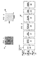
- Figure 1 illustrates a capacitor array 100 in which each large square 102 defines a unit capacitor and in which all capacitors with the same fill patterns belong to the same group.
- FIG. 2 is a flow diagram illustrating a capacitor array layout automation (CALA) procedure 200 according to one embodiment of the present invention.
- CALA procedure 200 is implemented to take advantage of capacitor repeatability characteristics associated with a capacitor array.
- CALA is a method that reduces the design cycle time by integrating all of the tasks that are necessary in manual generation of an array, and that solves difficulties associated with quality checking of the array and parasitic extraction, as stated herein before.
- CALA is implemented to provide a correct by construction array.
- each block shown in Figure 2 represents a particular task that is used to layout a capacitor array. Principles associated with each task are now set forth below in greater detail.
- Input block 202 receives all of the inputs 204-210 necessary to generate an array.
- These inputs 204-210 include design rules 204, user specific rules 206, X and Y dimensions of the active area(s) 208, and an array map file 210.
- Design rules 204 are the interlayer rules defined for a particular process. These rules 204 are used while drawing the rectangles to form a device in a layout cell. In a capacitor array, these rules 204 are necessary to draw all metal layers and also layers that are used to form a capacitor.
- User specific rules 206 are additional to the process design rules 204. These are the custom rules and can be specified by the user.
- X and Y of active area rules 208 are used to specify the active area associated with a capacitor. This information will be used while generating the unit capacitor cell.
- the array map file 210 serves as the basic and major input for the CALA procedure.
- Figure 3 is an array map file 300 associated with the unit capacitor distribution associated with the capacitor array 100 depicted in Figure 1.
- the array map file (e.g. 210, 300) is the ASCII representation of the capacitor distribution in an area having dimensions X by Y. If the array map file 210 is treated as a matrix, then the total number of capacitors in the array can be calculated by multiplying rows with columns. Multiplying the area of a unit capacitor cell by the total number of capacitors, the area of the array can be determined with the X and Y dimensions. Further, the total number of groups in a particular row can be defined simply by looking at the different numbers in the row.
- Element (1,1) for example, belongs to group 5 for the array map file 300, and should therefore be connected to the control line of group 5.
- a master data file is generated containing information such as location of each unit capacitor cell in an array, group name to which each unit capacitor cell belongs, and the total number of control lines that need to be routed between rows of capacitors, among other things.
- FIG. 4 illustrates a unit capacitor 400 employed in a commercially available capacitor array.
- Generation of a unit capacitor cell 400 is depicted as block 212 in Figure 2.
- X and Y dimensions of an active area provided by a user, total number of control lines available in the master data file discussed above, design and custom rules are used as the inputs for this block 212.
- X and Y co-ordinates are determined for all polygons. The design and custom rules are carefully considered during calculation of the co-ordinates.
- a unit capacitor cell 400 is than generated as shown in block 212.
- unit capacitor cell generation 212 array placement is performed as shown in block 214 in Figure 2. Co-ordinates for all of the capacitors to be placed in an array fashion are available in the master data file as stated herein before. Unit capacitor cell and the master data file provide the requisite inputs for this block 214. The top cell for which a name is specified by the user, is created in the given library. Having the origin as 0:0, all the unit capacitor cells are then placed in the layout cell. This top cell name is returned to the main module once the placement is complete.
- Bottom plate connectivity is next performed as shown in block 216 of Figure 2.
- Element numbers in each and every row are first mapped to a virtual number (e.g. 4 5 4 3 2 may be numbers from the array map file). Then, 3 4 3 2 1 can represent the virtual numbers for the row.
- This relates group numbers in a row to a specific set of numbers. For the instant case, the set of numbers includes 1, 2, 3 and 4.
- This process helps to ensure the control lines for the row are routed in ascending order and relates each element number with a row number. If the element number is 3 (virtual number) for example, then it should be connected to the third control line from the top.
- the location of a cut layer to be used for connecting two metal layers can be determined. This cut layer (vias or contact) is positioned at the determined location. All control lines that are spread across different rows are then connected to a main line, which completes the process of connecting the bottom plates to the control lines.
- Top plate connectivity is next performed as shown in block 218 of Figure 2 in which the top plates of all the unit capacitors are connected to a main top plate line.
- the width of this top plate line is determined by the custom rules provided by the user. Generally, the top plate line is very sensitive to noise, and so is shielded via a quiet line to minimize parasitics.
- signal names are generated as shown in block 220 of Figure 2, with the help of group numbers.
- Group number 3 for example, may be assigned a signal name such as control_3 that is connected to the third control line from the top.
- Signal names are thus placed on the main control lines, that are generated in the (Bottom Plate Connectivity) block 216.
- the location associated with placement of signal names are determined such that names will be placed for all control lines, which completes layout generation of the array.
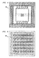
- Figure 5 illustrates a capacitor array layout 500 that employs the unit capacitor 400 depicted in Figure 4.
- the accuracy of the capacitor array layout 500 can be determined via a user-friendly report regarding parasitic extraction such as shown in block 222 of Figure 2.
- Parasitic extraction 222 includes generation of a detailed report on parasitics associated with all signal names in an array. Using a tool familiar to those skilled in the art, parasitics can be extracted from the final layout. Then, using custom scripts, information on parasitics with respect to each signal or node present in the array is generated to analyze the array regarding accuracy parameters.
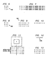
- Bottom plate connectivity associated with the capacitor array layout method 200 illustrated in Figure 2 is further explained herein below with reference to a 3-bit array map file 600 shown in Figure 6 as well as Figures 7-14. Specifically, method 200 generates all inputs necessary to implement a capacitor array layout from a given array map file, as discussed herein before.
- the numbers 1, 4, 5, 6 and 8 shown in array map file 600 represent different groups of capacitors in the array.
- the letter 'D' represents a dummy capacitor used for systematic spatial variation cancellation within the array.
- Figure 7 is a diagram illustrating a technique to determine the highest number of bottom plate control lines across all rows of the array map file 600 depicted in Figure 6 according to one embodiment of the present invention.
- the total number of bottom plate control lines is first determined for each row.
- the top row and middle row each have two control lines while the bottom row has three control lines.
- the highest number of bottom plate control lines across all rows for the array map file 600 is therefore three (3).
- FIG. 9 is a diagram illustrating a technique to replace each element in each row of the array map depicted in Figure 6 with its equivalent ascending number according to one embodiment of the present invention.
- the lowest number is five (5).
- the number 5 is therefore replaced with a one (1).
- the number 8 is replaced with a two (2); and the number 9 is replaced with a three (3). This technique is then repeated for each row separately as illustrated in Figure 9.
- Figure 10 is a simple diagram illustrating the first row of the array map file 600 depicted in Figure 6 in which each element is replaced with its equivalent ascending number as discussed herein above.
- FIG 11 is a pictorial diagram illustrating a method of bottom plate connectivity associated with the array map file 600 depicted in Figure 6 according to one embodiment of the present invention.
- the bottom plate of each capacitor in each row is connected to its respective control line that is achieved using the array map replaced with ascending numbers such as depicted in Figure 9.
- ascending numbers such as depicted in Figure 9.
- the first element of the top row is eight (8)
- its equivalent ascending number is two (2).
- Element 8 is therefore connected to the second control line from the top.
- the second element of the top row is five (5), it is connected to the first control line from the top because its equivalent ascending number is one (1).
- Both, array map 600 provided by the user, and array map 900 having equivalent ascending numbers are read together while connecting each bottom plate. In this way, if the algorithm reads 'D' in the original array map 600, it automatically connects that capacitor to the dummy line.
- Figure 12 is a diagram illustrating a technique to identify all unique numbers in an array for the array map file 600 depicted in Figure 6 according to one embodiment of the present invention. It can easily be seen that in the array 900, unique numbers are 1, 4, 5, 6, 8 and 9. This step is combined with additional steps described herein below to connect all of the vertical lines to the main control lines to remove all the opens created by horizontally routed control lines.
- Figure 13 is a diagram illustrating a technique to replace all elements of the array map file 600 depicted in Figure 6 with their respective position in the unique number list 1200 depicted in Figure 12 according to one embodiment of the present invention. Since array element 8 in the top row has position 5 in the unique number list 1200, for example, it is replaced with the number 5.
- Figure 14 is a pictorial diagram illustrating a horizontal line connectivity structure 1400 associated with the array map file 600 depicted in Figure 6 according to one embodiment of the present invention. It can be seen that the horizontal control line 1402 connected to array element 8 is now also connected to the fifth vertical line 1404. This same technique is then implemented for the remaining elements of the array to achieve the horizontal line connectivity structure 1400 depicted in Figure 14.
- the present invention is directed to an algorithmic technique to generate matched capacitor arrays used in A/D converter, D/A converters and programmable gain amplifiers, among other things.
- the technique implements automatic program-based generation of the array layout using templates to define the style of the layout such that any defined style of capacitor array can be generated.
- the method uses design rules of different processes to tailor the array for each specific case such that the layout is optimized for each process. Since each array can be generated from a particular electrical specification, multiple arrays within a common IC can be optimized for different purposes to preserve silicon area.
- an alternative method of automatically generating a matched capacitor array may comprise providing a capacitor array map file having different groups of capacitors in which each group other than a dummy capacitor group is associated with a distinct group number.
- the total number of distinct group numbers is determined for each row of the matched capacitor array and each dummy capacitor group within the array is associated with a distinct group number equal to the largest total number of distinct group numbers plus one.
- Each group within each row with an equivalent ascending number is replaced.
- Each ascending number within a row is determined by the distinct group numbers in step (b) and the distinct group number plus one in step (c).
- the ascending numbers range from one to the largest total number of distinct group numbers plus one.
- a matched capacitor array is implemented such that bottom plates associated with each distinct group of capacitors are connected to a respective control line. The ascending number associated with each distinct group of capacitor cells defines the control line that is connected to the bottom plates.
- Each control line may be connected to a respective main control line such that each main control line is substantially perpendicular to its connected control line, or each control line may be connected to a respective main control line by placing all distinct group numbers identified in step (a) and step (c) in ascending order such that each distinct group of capacitor cells can be defined by its position within the ascending order of distinct group numbers.
- Each control line may be connected to a respective main control line by placing each main control line such that it has a position relative to all other main control lines that is determined by the position within the ascending order of distinct group numbers.
- the method of automatically generating a matched capacitor array may comprise the additional steps of:
- a signal name is preferably generated for each main control line such that each main control line is associated with a distinct group number.
- the method may also comprise the step of extracting parasitic capacitance data from the array and analyzing array layout accuracy therefrom.
- the provided capacitor array design rules may comprise interlayer rules defined for a particular process.
- the unit capacitor cell x and y active area dimensions may comprise an ASCII representation of capacitor distribution in an area having dimensions x by y.
- a master data file may be created by generating a data file including location of each unit capacitor cell in an array, a group name to which each unit capacitor cell belongs, and a total number of control lines to be routed between rows of unit capacitor cells.
- the plurality of unit capacitor cells placed in array fashion may be used for creating a top cell having an origin designated as 0:0, and placing each unit capacitor cell therein.
Landscapes
- Engineering & Computer Science (AREA)
- Computer Hardware Design (AREA)
- Physics & Mathematics (AREA)
- Theoretical Computer Science (AREA)
- Evolutionary Computation (AREA)
- Geometry (AREA)
- General Engineering & Computer Science (AREA)
- General Physics & Mathematics (AREA)
- Design And Manufacture Of Integrated Circuits (AREA)
- Semiconductor Integrated Circuits (AREA)
- Analogue/Digital Conversion (AREA)
Applications Claiming Priority (2)
| Application Number | Priority Date | Filing Date | Title |
|---|---|---|---|
| US09/796,045 US6480137B2 (en) | 2001-02-28 | 2001-02-28 | Method of generating matched capacitor arrays |
| US796045 | 2001-02-28 |
Publications (2)
| Publication Number | Publication Date |
|---|---|
| EP1237181A2 true EP1237181A2 (de) | 2002-09-04 |
| EP1237181A3 EP1237181A3 (de) | 2005-07-27 |
Family
ID=25167125
Family Applications (1)
| Application Number | Title | Priority Date | Filing Date |
|---|---|---|---|
| EP02100193A Withdrawn EP1237181A3 (de) | 2001-02-28 | 2002-02-26 | Methode zur Erzeugung abgestimmter Kapazitätsnetzwerke |
Country Status (3)
| Country | Link |
|---|---|
| US (1) | US6480137B2 (de) |
| EP (1) | EP1237181A3 (de) |
| JP (1) | JP2002300032A (de) |
Families Citing this family (31)
| Publication number | Priority date | Publication date | Assignee | Title |
|---|---|---|---|---|
| US20030227402A1 (en) * | 2002-03-22 | 2003-12-11 | Sarnoff Corporation | Method and apparatus for reducing systematic errors in a current steering digital-to-analog converter |
| US6763509B2 (en) * | 2002-09-26 | 2004-07-13 | Sun Microsystems, Inc. | Method and apparatus for allocating decoupling capacitor cells |
| WO2004077677A1 (en) * | 2003-02-24 | 2004-09-10 | Analog Devices, Inc. | Signal-conditioning and analog-to-digital conversion circuit architecture |
| KR100794521B1 (ko) * | 2005-12-17 | 2008-01-16 | 삼성전자주식회사 | 커패시터 어레이 |
| US8386976B2 (en) * | 2007-02-15 | 2013-02-26 | United Microelectronics Corp. | Method for producing layout of semiconductor integrated circuit with radio frequency devices |
| US20080200132A1 (en) * | 2007-02-15 | 2008-08-21 | United Microelectronics Corp. | Method for producing layout of semiconductor integrated circuit with radio frequency devices |
| CN100552684C (zh) * | 2007-03-09 | 2009-10-21 | 联华电子股份有限公司 | 具有射频元件的半导体集成电路的布局方法 |
| US7705765B1 (en) * | 2008-10-10 | 2010-04-27 | Linear Technology Corporation | Systems and methods for characterizing component ratios and generating a digital representation of same |
| JP2011035210A (ja) * | 2009-08-03 | 2011-02-17 | Renesas Electronics Corp | 半導体集積回路、及び半導体集積回路のレイアウト方法 |
| US8692608B2 (en) | 2011-09-19 | 2014-04-08 | United Microelectronics Corp. | Charge pump system capable of stabilizing an output voltage |
| US9030221B2 (en) | 2011-09-20 | 2015-05-12 | United Microelectronics Corporation | Circuit structure of test-key and test method thereof |
| US8395455B1 (en) | 2011-10-14 | 2013-03-12 | United Microelectronics Corp. | Ring oscillator |
| US8421509B1 (en) | 2011-10-25 | 2013-04-16 | United Microelectronics Corp. | Charge pump circuit with low clock feed-through |
| US8588020B2 (en) | 2011-11-16 | 2013-11-19 | United Microelectronics Corporation | Sense amplifier and method for determining values of voltages on bit-line pair |
| US8493806B1 (en) | 2012-01-03 | 2013-07-23 | United Microelectronics Corporation | Sense-amplifier circuit of memory and calibrating method thereof |
| US8970197B2 (en) | 2012-08-03 | 2015-03-03 | United Microelectronics Corporation | Voltage regulating circuit configured to have output voltage thereof modulated digitally |
| US8724404B2 (en) | 2012-10-15 | 2014-05-13 | United Microelectronics Corp. | Memory, supply voltage generation circuit, and operation method of a supply voltage generation circuit used for a memory array |
| US8669897B1 (en) | 2012-11-05 | 2014-03-11 | United Microelectronics Corp. | Asynchronous successive approximation register analog-to-digital converter and operating method thereof |
| US8711598B1 (en) | 2012-11-21 | 2014-04-29 | United Microelectronics Corp. | Memory cell and memory cell array using the same |
| US8873295B2 (en) | 2012-11-27 | 2014-10-28 | United Microelectronics Corporation | Memory and operation method thereof |
| US8643521B1 (en) | 2012-11-28 | 2014-02-04 | United Microelectronics Corp. | Digital-to-analog converter with greater output resistance |
| US9030886B2 (en) | 2012-12-07 | 2015-05-12 | United Microelectronics Corp. | Memory device and driving method thereof |
| US8953401B2 (en) | 2012-12-07 | 2015-02-10 | United Microelectronics Corp. | Memory device and method for driving memory array thereof |
| US8917109B2 (en) | 2013-04-03 | 2014-12-23 | United Microelectronics Corporation | Method and device for pulse width estimation |
| US9105355B2 (en) | 2013-07-04 | 2015-08-11 | United Microelectronics Corporation | Memory cell array operated with multiple operation voltage |
| US8947911B1 (en) | 2013-11-07 | 2015-02-03 | United Microelectronics Corp. | Method and circuit for optimizing bit line power consumption |
| US8866536B1 (en) | 2013-11-14 | 2014-10-21 | United Microelectronics Corp. | Process monitoring circuit and method |
| US9143143B2 (en) | 2014-01-13 | 2015-09-22 | United Microelectronics Corp. | VCO restart up circuit and method thereof |
| US10628544B2 (en) * | 2017-09-25 | 2020-04-21 | International Business Machines Corporation | Optimizing integrated circuit designs based on interactions between multiple integration design rules |
| CN107863966B (zh) * | 2017-10-31 | 2021-02-05 | 电子科技大学 | 一种用于智能传感器的逐次逼近模数转换器电容优化方法 |
| US10783296B1 (en) * | 2018-06-08 | 2020-09-22 | Diakopto, Inc. | Matched net and device analysis based on parasitics |
Family Cites Families (10)
| Publication number | Priority date | Publication date | Assignee | Title |
|---|---|---|---|---|
| US4399426A (en) * | 1981-05-04 | 1983-08-16 | Tan Khen Sang | On board self-calibration of analog-to-digital and digital-to-analog converters |
| US5353028A (en) * | 1992-05-14 | 1994-10-04 | Texas Instruments Incorporated | Differential fuse circuit and method utilized in an analog to digital converter |
| US5235335A (en) * | 1992-06-02 | 1993-08-10 | Texas Instruments Incorporated | Circuit and method for tuning capacitor arrays |
| US5322438A (en) * | 1993-06-18 | 1994-06-21 | Silicon Systems, Inc. | Layout scheme for precise capacitance ratios |
| DE69509851T2 (de) * | 1994-09-30 | 1999-09-30 | Sharp K.K., Osaka | Kapazitätserzeugungsverfahren |
| US5761080A (en) * | 1995-11-22 | 1998-06-02 | International Business Machines Corporation | Method and apparatus for modeling capacitance in an integrated circuit |
| US5973633A (en) * | 1996-12-20 | 1999-10-26 | Texas Instruments Incorporated | Weighted capacitor array with selective grouping to form array elements |
| KR100252647B1 (ko) * | 1997-06-17 | 2000-04-15 | 윤종용 | 스위치/커패시터어레이를구비한아날로그/디지털변환기 |
| US6016019A (en) * | 1998-05-28 | 2000-01-18 | Microchip Technology Incorporated | Capacitor array arrangement for improving capacitor array matching |
| US6225678B1 (en) * | 1998-12-23 | 2001-05-01 | Microchip Technology Incorporated | Layout technique for a matching capacitor array using a continuous top electrode |
-
2001
- 2001-02-28 US US09/796,045 patent/US6480137B2/en not_active Expired - Lifetime
-
2002
- 2002-02-15 JP JP2002037737A patent/JP2002300032A/ja active Pending
- 2002-02-26 EP EP02100193A patent/EP1237181A3/de not_active Withdrawn
Also Published As
| Publication number | Publication date |
|---|---|
| EP1237181A3 (de) | 2005-07-27 |
| US20020118130A1 (en) | 2002-08-29 |
| JP2002300032A (ja) | 2002-10-11 |
| US6480137B2 (en) | 2002-11-12 |
Similar Documents
| Publication | Publication Date | Title |
|---|---|---|
| US6480137B2 (en) | Method of generating matched capacitor arrays | |
| US5638293A (en) | Optimal pad location method for microelectronic circuit cell placement | |
| US6815811B2 (en) | Semiconductor integrated circuit with dummy patterns | |
| US7765509B2 (en) | Auto connection assignment system and method | |
| JPH04211154A (ja) | 半導体集積回路のレイアウト方法 | |
| KR101300968B1 (ko) | 제조 조건 판정 방법, 제조 조건 판정 장치, 마운터 및프로그램 | |
| US20120217988A1 (en) | Flexible test fixture | |
| WO1999039287A1 (en) | Method and system for porting an integrated circuit layout from a reference process to a target process | |
| US6976236B1 (en) | Method for automatically routing connections between top side conductors and bottom side conductors of an integrated circuit package | |
| US11157676B2 (en) | Method for routing bond wires in system in a package (SiP) devices | |
| CN115394671B (zh) | 抓取对象引脚的方法、测试芯片及其设计方法、系统 | |
| Yu et al. | Device array layout synthesis with nonlinear gradient compensation for a high-accuracy current-steering DAC | |
| CN114611452A (zh) | 基于电路原理图在版图中自动生成Sub Cell的方法 | |
| US7496878B2 (en) | Automatic wiring method and apparatus for semiconductor package and automatic identifying method and apparatus for semiconductor package | |
| US20200302105A1 (en) | Analog design tool having a cell set, and related methods | |
| US20020174410A1 (en) | Method of configuring integrated circuits using greedy algorithm for partitioning of n points in p isothetic rectangles | |
| US7370303B2 (en) | Method for determining the arrangement of contact areas on the active top side of a semiconductor chip | |
| JP3119631B2 (ja) | 半導体集積回路装置及びその設計方法 | |
| US6862722B2 (en) | Extendable method for revising patterned microelectronic conductor layer layouts | |
| US7397256B2 (en) | Automatic design method for semiconductor device | |
| KR20250152383A (ko) | 반도체 공정 흐름의 분석을 지원하는 전자 장치 및 전자 장치의 동작 방법 | |
| US20250094682A1 (en) | Analog ECO Flow | |
| CN121031517A (zh) | 基于矩阵建模与匈牙利算法的超大规模集成电路标准单元电源地网络的布线约束识别方法 | |
| US7055122B1 (en) | Method for automatically connecting top side conductors with bottom side conductors of an integrated circuit package | |
| JP2803800B2 (ja) | 半導体集積回路装置の配線方法 |
Legal Events
| Date | Code | Title | Description |
|---|---|---|---|
| PUAI | Public reference made under article 153(3) epc to a published international application that has entered the european phase |
Free format text: ORIGINAL CODE: 0009012 |
|
| AK | Designated contracting states |
Kind code of ref document: A2 Designated state(s): AT BE CH CY DE DK ES FI FR GB GR IE IT LI LU MC NL PT SE TR |
|
| AX | Request for extension of the european patent |
Free format text: AL;LT;LV;MK;RO;SI |
|
| PUAL | Search report despatched |
Free format text: ORIGINAL CODE: 0009013 |
|
| AK | Designated contracting states |
Kind code of ref document: A3 Designated state(s): AT BE CH CY DE DK ES FI FR GB GR IE IT LI LU MC NL PT SE TR |
|
| AX | Request for extension of the european patent |
Extension state: AL LT LV MK RO SI |
|
| AKX | Designation fees paid | ||
| REG | Reference to a national code |
Ref country code: DE Ref legal event code: 8566 |
|
| STAA | Information on the status of an ep patent application or granted ep patent |
Free format text: STATUS: THE APPLICATION IS DEEMED TO BE WITHDRAWN |
|
| 18D | Application deemed to be withdrawn |
Effective date: 20060128 |