Technical Field:
The present invention relates to a method for inspecting a silicon
wafer (hereinafter may be simply referred to as a "wafer"), and more
specifically to a method for inspecting a silicon wafer for detecting a new
defect which has not been identified, a method for manufacturing a silicon
wafer having no such defect, a method for fabricating a semiconductor device
using the silicon wafer having no such defect above, and the new silicon wafer
having no such defect.
Background Art:
Generally a method for manufacturing a silicon wafer comprises a
slicing step of slicing a single crystal ingot to obtain a thin disk-shaped wafer;
a chamfering step of chamfering a peripheral edge portion of the wafer
obtained through the slicing step to prevent cracking and chipping of the
wafer; a lapping step of flattening this wafer; an etching step of removing
machining deformation remaining in the so chamfered and lapped wafer; a
polishing step of making a mirror surface of the wafer; and a cleaning step of
cleaning the polished wafer to remove a polishing agent or dust particles
deposited thereon. Only the main steps are listed above, and sometimes
other steps such as a heat treatment step may be added, or the step sequence
may be changed. The silicon wafer manufactured as described above is
finally subjected to a quality check, then is packaged in a container for
accommodating wafers therein, and is sent to a device fabricating company
(or step).
With the manufacturing steps as described above, recently in
association with the tendency that devices have been becoming more and
more minute, demands for device performance to be achieved have become
increasingly severe, and further the silicon wafer is required to have
completeness of the crystal quality and cleanliness of the wafer surface.
To satisfy the demands, it is necessary to evaluate quality of the
silicon wafer under stringent conditions, and to improve the processing for
manufacturing the silicon wafer and fabricating the device using the silicon
wafer therein.
In the silicon wafer, completeness of the crystal quality is largely
spoiled by existence of impurities, microdefects, strain fields and so on. On
the silicon wafer surface, heavy metals, organic materials, particles and
surface roughness also cause problems.
As a defect causing a problem in a device fabricating process, there
has been known a COP (Crystal Originated Particle) appearing in the
vicinity of a surface layer of the wafer. The COP is generally defined as a
defect with the size of 0.1 µm or less, but it appears on the wafer surface as a
pit, that is, a defect with the size on the order of 0.1 to 0.5 µm which can be
observed by processing the wafer with an ammonia-hydrogen peroxide
solution (also referred to as a "SCl solution"). These are defects generated
when the crystal is pulled.
A FPD (Flow Pattern Defect) having closely related to an oxide film
dielectric breakdown strength is a ripple-like defect appearing when
preferential etching is performed with an etching liquid based on
hydrofluoric acid and potassium bichromate.
There have been known other defects such as a LSTD (Laser
Scattering Tomography Defect) detected by the laser scattering tomography,
and these defects are microdefects having similar behavior during growth of
the crystal.
Further it is known that such defects as an OSF (Oxidation-induced
Staking Fault) largely affect performance of a device.
To evaluate these defects, generally preprocessing is performed to a
silicon wafer itself prior to start of the evaluation, and then the defects are
directly monitored visually, with an electronic microscope or the like.
Disclosure of the Invention:
It has been considered that there may exist other defects affecting
the device fabricating step in addition to those described above. It is
generally considered that the defects are of different types from the COP,
FPD, LSTD, and OSF, but particular features of the defects have not been
clarified.
Therefore it has been difficult to accurately and finely evaluate
quality of a silicon wafer and to improve the processes for manufacturing the
silicon wafer and fabricating a device.
The present inventor has discovered a new type of defect having the
entire defect size of 0.5 µm or more which is different from the crystal
defects of the silicon wafer such as a COP previously known and in which
microdefects gather in a colony state. This defect may especially affect a
yield in the device fabricating step.
This new type of defect is described in more details below. There is
no difference between irregularities in the defect area and those in other area
of the silicon surface. For instance, this defect can not be detected with an
AFM (Atomic Force Microscope) at all.
An atomic force microscope (AFM) monitors a surface by making use
of atomic forces working when atoms at the tip of the probe are approached to
a sample and controlling the probe for keeping the atomic forces at a constant
level. The resolution of the atomic force microscope (AFM) is 0.1 nm or below.
This new type of defect can be detected by performing appropriate
image processing with a laser microscope based on a confocal optical system.
The confocal optical system detects quantities of light having passed
through a pinhole by irradiating converged light beams on a fine spot on a
sample and re-converging the reflected light to the pinhole fitted to the front
of a light receiver.
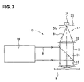
As shown in Fig. 7, a laser microscope 10 based on this confocal
optical system comprises a laser light source 14 such as an argon ion laser, a
light detector 24 such as a photodiode, a beam splitter 16, a pinhole 20a and
others. This laser microscope 10 is described in detail later.
This new type of defect can also be evaluated by cleaning with a SC1
solution. However, this evaluation method becomes problematically a
destructive inspection. Further to achieve an easy observation by cleaning
with the SCl solution, the etching time is desired to be longer, but as etching
proceeds, the wafer surface becomes rougher, so that the new defect
discovered in the present invention can hardly be differentiated from the
COP.
As the newly discovered defect described above gives influence on a
yield in the device fabricating step, it has been found that the wafer having a
defect evaluated and observed by the evaluation method described above
should not be sent to the device fabricating step. The present invention has
been completed based on the finding.
It is an object of the present invention to provide a method for
inspecting a silicon wafer making it possible to identify and efficiently detect
a new type of defect affecting a device fabricating step, a method for
manufacturing a silicon wafer not having the defect as described above, a
method for fabricating a semiconductor device using the silicon wafer not
having the defect as described above, and the silicon wafer not having the
defect itself.
To solve the problems described above, a method for inspecting a
silicon wafer according to the present invention comprises the step of, when
inspecting the silicon wafer, inspecting a defect having the entire defect size
of 0.5 µm or more in which microdefects gather in a colony state. In this new
type of defect, several tens to several hundreds microdefects each having the
size on the order of 0.05 to 0.5 µm gather to form a colony-like defect.
Depending on the number of gathering microdefects, even the small defect is
detectable as one having the size of at least 0.5 µm. There may be found the
large defect having the size on the order of 3 to 10 µm.
The defect can be inspected with a laser microscope based on a
confocal optical system or a dark field microscope. There is no difference
between irregularities in the defect area and those in other area of the wafer
surface; therefore the defect can not be evaluated with an atomic force
microscope (AFM). After preprocessing is performed with an
ammonia-hydrogen peroxide solution (a SC1 solution) and the defect area is
etched, the defect may be evaluated and detected, but in this case the
inspection becomes a destructive one. Further this type of defect can hardly
be differentiated from the conventional type of defect such as a COP. For
evaluation as a non-destructive inspection, it is preferable to perform the
inspection with the laser microscope based on the confocal optical system.
It has been found that, in addition to the laser microscope based on
the confocal optical system, also a dark field microscope can be used for the
evaluation. The dark field microscope is used for observing light scattered by
defects or particles when irradiating laser beams on a sample to be monitored
in the state where the entire measurement system is placed under a dark
condition, and also this dark field microscope can be used for the evaluation
as a non-destructive inspection.
A first aspect of a method for manufacturing a silicon wafer
according to the present invention comprises the steps of polishing the
silicon wafer; cleaning and drying the polished silicon wafer; and inspecting a
defect having the entire defect size of 0.5 µ m or more in which microdefects
gather in a colony state with a laser microscope based on a confocal optical
system or a dark field microscope after the cleaning and drying step.
A second aspect of a method for manufacturing a silicon wafer
according to the present invention comprises the steps of: mirror polishing
the silicon wafer; cleaning and drying the mirror polished silicon wafer; and
preventing deposition of impurities on a surface of the wafer and also
generation of a defect having the entire defect size of 0.5 µm or more in
which microdefects gather in a colony state after the wafer is mirror polished.
A method for fabricating a semiconductor device according to the
present invention comprises the steps of: inspecting a defect having the
entire defect size of 0.5 µm or more in which microdefects gather in a colony
state in a silicon wafer; selecting the silicon wafer not having the defect; and
fabricating the semiconductor device by using the silicon wafer not having
the defect.
A silicon wafer according to the present invention is the silicon wafer
which is mirror polished and has no defect having the entire defect size of 0.5
µm or more in which microdefects gather in a colony state.
This new type of defect to be inspected by the inspecting method
according to the present invention is different from any crystal defect, and is
conceivably generated by contamination by impurities generated in the
polishing step and afterward such as metallic impurities, a non-uniform
surface state after polishing (such as the state where alkaline components of
a polishing agent remain partially on the surface or hydrophilic areas and
hydrophobic areas have been generated), or deposition of silicon particles or
other particles floating in the air. Generation of this type of defect can be
prevented by preventing deposition of impurities on the wafer surface after
polishing.
Therefore, to manufacture a wafer not having the defect as described
above, it is required to prevent deposition of impurities immediately after the
wafer is polished. For instance, storage of a just polished wafer is conducted
in water and the storage water is controlled to manufacture the wafer by
adding citric acid and a surfactant, a hydrogen peroxide solution and citric
acid, or the like for preventing metals as a kind of the impurities from being
deposited on a surface of the wafer. While a final wafer is manufactured,
after the storage described above, through several steps including a cleaning
step and a packaging step (and an inspecting step), contamination may occur
by impurities from the atmosphere during the cleaning and packaging steps
after the polishing step, or from, for instance, a container for shipment used
for shipping the wafer product, so in the wafer manufacturing process careful
attentions are required for preventing the contamination as described above.
By paying careful attentions for preventing contamination by
impurities after the polishing step, a wafer not having these defects can be
constantly manufactured.
Apart from the above-described wafer manufacturing method, it is
also desirable to include a step for inspecting a defect having the entire defect
size of 0.5µm or more in which microdefects gather in a colony state with a
laser microscope based on a confocal optical system or a dark field microscope
in the manufacturing process and especially to include the inspecting step
after the polishing step but before the packaging step.
When the inspecting step is included in the manufacturing process,
a wafer which may lower a yield can preferably be removed. Further the
laser microscope based on the confocal optical system or the dark field
microscope enables a non-destructive inspection, so that the inspecting step
can be performed as a part of the general manufacturing process.
By selecting a wafer not having the defect having the entire defect
size of 0.5 µm or more as described above in which microdefects gather in a
colony state, it is possible to fabricate a device by using the wafer in the
device manufacture process with a high yield.
Brief Description of the Drawings:
Fig. 1 is a micrograph showing a silicon wafer taken by a laser
microscope based on a confocal optical system in Experimental Example 1;
Fig. 2 is a schematic view showing the silicon wafer in Fig. 1;
Fig. 3 is a micrograph showing a silicon wafer taken by an atomic
force microscope (AFM) in Experimental Example 1;
Fig. 4 is a schematic view showing the silicon wafer in Fig. 3;
Fig. 5 is a micrograph showing a silicon wafer taken by an atomic
force microscope (AFM) in Experimental Example 2;
Fig. 6 is a schematic view showing the silicon wafer in Fig. 5;
Fig. 7 is a general explanatory view showing a basic structure of the
laser microscope based on the confocal optical system;
Fig. 8 is a flow chart showing one embodiment of procedures for
inspecting the wafer;
Fig. 9 is a general explanatory view showing a basic structure of a
dark field microscope;
Fig. 10 is a micrograph showing a silicon wafer taken by the dark
field microscope in Experimental Example 3; and
Fig. 11 is a schematic view showing the silicon wafer in Fig. 10.
Best Mode for Carrying Out the Invention:
A laser microscope based on a confocal optical system and a dark
field microscope used in the method according to the present invention and
procedures for inspecting a wafer with the microscopes are described with
reference to Fig. 7, Fig. 8, and Fig. 9, but it is to be noted that the present
invention is not limited to the embodiments shown in these figures, and it is
needless to say that various modifications are possible within the scope of the
technical idea of the present invention.
Fig. 7 is a general explanatory view showing a basic structure of a
laser microscope based on a confocal optical system. In Fig. 7, the reference
numeral 10 indicates a laser microscope based on a confocal optical system,
in which a laser beam source 14 such as an argon laser is provided at a
position opposite to a microscope body 12.
The microscope body 12 comprises a beam splitter 16 for splitting
laser beams B from the laser beam source 14 to a plurality of laser beams B,
an object lens 18 for converging the laser beams B onto a surface of a wafer W
to be inspected, a converging lens 22 for converging the laser beams B
reflected from a surface of the wafer W into a pinhole 20a of a pinhole
member 20, and a light detector 24 for receiving the laser beams B having
passed through the pinhole 20a.
With the configuration as described above, now the principle of
operations thereof is described below.
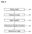
Procedures for inspecting the wafer W with the laser microscope 10
based on the confocal optical system described above are described below
with reference to Fig. 8. Fig. 8 is a flow chart showing one embodiment of
procedures for inspecting the wafer W.
More specifically, the wafer inspecting procedures in the wafer
inspecting method according to the present invention are as described below.
When an optional video printer is used together with the laser
microscope based on the confocal optical system used in Examples described
below, it is possible to print out a monitor screen. Further the defect area
detected as described above can also be analyzed from different points of view
by converting the coordinate file format reflecting a result of inspection to a
coordinate file format for other devices such as a scanning electron
microscope (SEM) or an atomic force microscope (AFM).
Fig. 9 is a general explanatory view showing a basic structure of a
dark field microscope. In Fig. 9, the reference numeral 30 indicates a dark
field microscope, and the dark field microscope 30 has an optical microscope
body 32 with the measurement system set in a dark field. A laser beam
source 34 such as an argon laser is provided in relation to the optical
microscope body 32. When the laser beams B from the laser beam source 34
are irradiated onto a surface of the wafer W, the laser beams B are scattered
due to a defect 1 and the like of the wafer W, and the scattered laser beams S
are again converged and detected by a monitoring unit (detector) 44 such as a
CCD camera.
With the configuration as described above, now the principle of
operations thereof is described below.
Examples
The present invention will be described more specifically below by
way of following Examples which should be construed as illustrative rather
than restrictive.
[Experimental Example 1: Inspection with a laser microscope based on a
confocal optical system (Non-destructive inspection) ]
A silicon wafer was monitored and inspected with the MAGICS
(product name) made by LASERTEC CORP. as a laser microscope based on a
confocal optical system. The inspection carried out with the laser microscope
based on the confocal optical system is not destructive, and any specific
preprocessing is not required.
The sample silicon wafer was manufactured by the general method.
Namely, silicon single crystal ingot was sliced, and a peripheral edge portion
of the sliced wafer was chamfered to prevent cracking and chipping thereof.
The wafer was lapped to be flattened, etched to remove machining
deformation, polished for making a mirror surface of the wafer, cleaned and
dried. The cleaned and dried sample wafer was evaluated.
A result of monitoring the defects is shown in Fig. 1 and Fig. 2. Fig.
1 is a micrograph showing a surface of the sample silicon wafer taken with
the MAGICS, and Fig. 2 is a schematic view showing the silicon wafer in Fig.
1. The reference numeral 1 in Fig. 1 and Fig. 2 indicates a defect (defect 1)
which may cause troubles in the device fabricating process. From the
micrograph of Fig. 1 and the schematic view of Fig. 2, it is understood that
dot-like defects gather in the colony state to form a defect area with the size
of 0.5µm or more as a whole. The defect 1 shown in Fig. 1 and Fig. 2
indicates a representative defect observed on a wafer surface. The entire size
of each defect varies according to the gathering state of the microdefects, but
a plurality of defects 1 each having the similar colony-like form and the size
on the order of 0.5µm to 10µm were observed on the wafer surface. The size
of the defect 1 shown in Fig. 1 and Fig. 2 was about 6µm.
The reference numeral 2 in Fig. 1 and Fig. 2 indicates a defect
(defect 2) which can be observed with an atomic force microscope (AFM).
This defect 2 was used as a mark so that the defect 2 could be confirmed at
the same position also in other evaluation methods. Namely, monitoring was
performed under a fixed point observation.
Then irregularities of the defect surface were evaluated with the
atomic force microscope (AFM). The SPA 360 from SEIKO INSTRUMENTS
INC. was used as the atomic force microscope (AFM).
Using the defect 2 as a mark, the defect was confirmed at the same
position in Fig. 1 and Fig. 2. A result of monitoring with the atomic force
microscope (AFM) is shown in Fig. 3. Fig. 3 is a micrograph showing a
surface of the silicon wafer taken with the SPA 360, while Fig. 4 is a
schematic view showing the silicon surface in Fig. 3. As clearly understood
from Fig. 3 and Fig. 4, the defect 1 observed in Fig. 1 and Fig. 2 could not be
detected even when irregularities of the wafer surface were monitored with
the atomic force microscope (AFM), and it is considered that this defect has
no irregularities and that this defect is caused by impurities gathering in a
strained portion within the wafer (an uppermost surface layer).
[Experimental Example 2: Inspection after long time processing with a SC1
solution (Destructive inspection)]
The silicon wafer observed in Experimental Example 1 was
processed with a SC1 solution (a chemical solution with the volumetric ratio
of 28 wt % ammonia water: 30 wt % hydrogen peroxide solution: water = 10 :
2 : 100) for 40 minutes under the solution temperature of 80 °C. The wafer
immersed in the solution was then monitored and inspected with an atomic
force microscope (AFM).
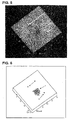
A result of observation of the defect is shown in Fig. 5 and Fig. 6. Fig.
5 is a micrograph showing a surface of the silicon wafer taken with the SPA
360, while Fig. 6 is a schematic view showing the surface of silicon wafer
shown in Fig. 5. The area of defect 1 not observed with the atomic force
microscope (AFM) (see Fig. 3 and Fig. 4) was etched with a chemical solution
with the SC1 composition, and the defect 1 could be observed as shown in Fig.
5 and Fig. 6.
As described above, this new defect 1 is different from a defect
caused due to the crystalline structure such as a COP, and it can be
considered that this defect is caused due to any defect in an uppermost
surface layer of the wafer surface, especially strain therein.
[Experimental Example 3: Inspection with a dark field microscope]
A silicon wafer was observed with the SPA 360 from SEIKO
INSTRUMENTS INC. as a dark field microscope. This SPA 360 is a unit
provided with different two types of microscopes, namely the atomic force
microscope (AFM) and the dark field microscope, and this unit enables
observation with a dark field microscope at the same position where
measurement is performed with the AFM.
The sample silicon wafer was a wafer with a defect having the entire
defect size of 0.5µm or more in which microdefects gather in a colony state
(the wafer used in Experimental Example 1), and the defect was confirmed
with a laser microscope based on the confocal optical system.
A result of observation of the defect is shown in Fig. 10 and Fig. 11.
Fig. 10 is a micrograph showing the silicon wafer taken with a dark field
microscope, while Fig. 11 is a schematic view showing the silicon wafer
shown in Fig. 10. Observation was performed at about × 50 magnification.
Although the microdefects can not be differentiated from each other, these
figures show that the defect having the same form as that of the defect 1
observed with the laser microscope based on the confocal optical system can
be observed. A defect having the ordinary irregularities (such as the defect 2
observed as a mark) or a particle can be detected with the dark field
microscope because scattering of the laser beams occurs, but it was found
that also the defect having no irregularities found in the present invention
could be observed with the dark field microscope. It can be considered that
this new type of defect can be observed with the dark field microscope
because this defect is a specific one. Namely, although this defect has no
irregularities, it can be considered that the defect reflects a difference in
surface quality between the defect area and other normal area in the vicinity
thereof, especially a difference in density due to impurities present on the
wafer surface.
(Example 1)
A sample silicon wafer subjected up to the polishing step by
following the same sequence as that in Experimental Example 1 was
prepared, and the polished sample wafer was stored in a pit tank containing
citric acid and hydrogen peroxide solution to prevent impurities such as
metal contamination as much as possible, and then was subjected to the
cleaning step. Contamination by heavy metals was prevented also during
this cleaning step, and then the sample was dried. Even after the steps
described above, the sample was kept under an environment where the
quantities of particles in the atmospheric air were 1000 pieces per cubic feet
or less, and the sample wafer was monitored and evaluated with a laser
microscope based on a confocal optical system immediately after the sample
was taken out from the environment. The defect 1 having the entire defect
size of 0.5 µm or more in which microdefects gather in a colony state as
shown in Fig. 1 was not observed.
(Comparative Example 1)
A sample silicon wafer subjected up to the polishing step by
following the same sequence as that in Experimental Example 1 was
prepared, and the polished sample wafer was stored in pure water, took out
from the water and left intentionally under the atmospheric air for a while,
and then was cleaned. In these steps, the sample wafer was intentionally
contacted to unspecified impurities. Then the sample silicon wafer was
monitored and evaluated with a laser microscope based on a confocal optical
system. A plurality of defects 1 having the entire defect size of 0.5 µm or
more in which microdefects gather in a colony state as shown in Fig. 1 and
Fig. 2 were observed. In the wafers (8-inch wafer) observed as described
above, 10 to 30 colony-like defects each having the size on the order of 1 to 5
µm were present on a surface of the wafer, especially in the peripheral area
thereof.
(Manufacturing Example 1)
The wafer manufacturing process described hereinafter comprises a
step for inspecting a defect having the entire defect size of 0.5 µm or more in
which microdefects gather in a colony state with a laser microscope based on
a confocal optical system, and the inspecting step was located between a
cleaning and drying step and a packaging step.
Steps up to the cleaning and drying step in the wafer manufacturing
process were carried out in a plurality of lines to evaluate wafers. The
above-described defect was observed in some lines, but was not observed in
other lines. In the manufacturing process wherein the defect was observed,
the water used for storing a polished wafer was only pure water. When
hydrogen peroxide solution and citric acid were added to the water for storing
wafers therein, the defect was not observed in the wafer manufactured in the
line. As described above, the manufacturing process can be improved by the
use of the result obtained in the inspection step with the laser microscope
based on the confocal optical system.
When the wafer recognized as having a defect, especially a wafer
having the relatively larger defect with the size of 0.5 µm or more was used
in the device fabricating process, the yield became lower. In the inspecting
step, the defect was recognized visually or by the image processing, and
wafers not having the defect were selected and used in the device fabricating
process, so that the yield was improved.
From the results of various experiments described above, a new
defect affecting the yield in the device fabricating process was found. It was
also confirmed that the wafer not having the defect as described above
showed the excellent performance. Further it was found that the defect could
easily be found with a laser microscope based on a confocal optical system.
Therefore by selecting only wafers not having the defect and sending the
selected wafers to the device fabricating process, the yield can be improved.
It was also found that it was required to prevent and control contamination
by impurities after polishing for protection against this type of defect. Also it
was found that the defect could be detected, in addition to the laser
microscope based on the confocal optical system, also with a dark field
microscope, and that, in that case, the same effect as that obtained by the
laser microscope could be obtained. It is preferable to use a microscope
capable of sensing a change in a quantity of detected light (difference in
contrast).
It is to be noted that the present invention is not limited to the
embodiments described above. For instance, the defect which can be
observed with the laser microscope based on the confocal optical system or
the like, namely the defect without irregularities having the entire defect size
of 0.5 µm or more in which microdefects gather in a colony state is often
observed after the polishing step. It can be considered that, as a surface of a
polished wafer is in an active state, the surface is easily affected when the
surface is contacted to impurities which are considered to be a cause for the
defect. The active state of the wafer surface is also generated after epitaxial
growth or on a surface of a wafer processed by, for instance, a hydrofluoric
acid solution, with the result that similar defects may be observed.
Inspection of wafers after epitaxial growth or wafers processed by
hydrofluoric acid and selection of wafers having no defect after these steps
are also included in a technical scope of the present invention.
Capability of Exploitation in Industry:
As described above, with the method for inspecting a silicon wafer
according to the present invention, it is possible to efficiently detect and
identify a new defect of a silicon wafer which may affect a device fabricating
process (a defect having the entire defect size of 0.5 µm or more in which
microdefects gather in a colony state). With the method for manufacturing a
silicon wafer according to the present invention, a wafer not having this new
type of defect can be manufactured. Further with the method for fabricating
a device according to the present invention, the yield in the device fabricating
process can be improved by using a silicon wafer not having this new type of
defect. The silicon wafer according to the present invention does not have
this new type of defect, and can contribute to improvement of yield in the
device fabricating process.