EP1231801B1 - Appareil de communication sans fil à traitement de données intermittent - Google Patents
Appareil de communication sans fil à traitement de données intermittent Download PDFInfo
- Publication number
- EP1231801B1 EP1231801B1 EP20010113086 EP01113086A EP1231801B1 EP 1231801 B1 EP1231801 B1 EP 1231801B1 EP 20010113086 EP20010113086 EP 20010113086 EP 01113086 A EP01113086 A EP 01113086A EP 1231801 B1 EP1231801 B1 EP 1231801B1
- Authority
- EP
- European Patent Office
- Prior art keywords
- signal
- signal processing
- control
- processing block
- wireless communication
- Prior art date
- Legal status (The legal status is an assumption and is not a legal conclusion. Google has not performed a legal analysis and makes no representation as to the accuracy of the status listed.)
- Expired - Lifetime
Links
Images


Classifications
-
- H—ELECTRICITY
- H04—ELECTRIC COMMUNICATION TECHNIQUE
- H04W—WIRELESS COMMUNICATION NETWORKS
- H04W52/00—Power management, e.g. TPC [Transmission Power Control], power saving or power classes
- H04W52/02—Power saving arrangements
- H04W52/0209—Power saving arrangements in terminal devices
- H04W52/0225—Power saving arrangements in terminal devices using monitoring of external events, e.g. the presence of a signal
- H04W52/0229—Power saving arrangements in terminal devices using monitoring of external events, e.g. the presence of a signal where the received signal is a wanted signal
-
- H—ELECTRICITY
- H04—ELECTRIC COMMUNICATION TECHNIQUE
- H04W—WIRELESS COMMUNICATION NETWORKS
- H04W52/00—Power management, e.g. TPC [Transmission Power Control], power saving or power classes
- H04W52/02—Power saving arrangements
-
- H—ELECTRICITY
- H04—ELECTRIC COMMUNICATION TECHNIQUE
- H04W—WIRELESS COMMUNICATION NETWORKS
- H04W52/00—Power management, e.g. TPC [Transmission Power Control], power saving or power classes
- H04W52/02—Power saving arrangements
- H04W52/0209—Power saving arrangements in terminal devices
- H04W52/0261—Power saving arrangements in terminal devices managing power supply demand, e.g. depending on battery level
- H04W52/0274—Power saving arrangements in terminal devices managing power supply demand, e.g. depending on battery level by switching on or off the equipment or parts thereof
- H04W52/028—Power saving arrangements in terminal devices managing power supply demand, e.g. depending on battery level by switching on or off the equipment or parts thereof switching on or off only a part of the equipment circuit blocks
- H04W52/0283—Power saving arrangements in terminal devices managing power supply demand, e.g. depending on battery level by switching on or off the equipment or parts thereof switching on or off only a part of the equipment circuit blocks with sequential power up or power down of successive circuit blocks, e.g. switching on the local oscillator before RF or mixer stages
-
- Y—GENERAL TAGGING OF NEW TECHNOLOGICAL DEVELOPMENTS; GENERAL TAGGING OF CROSS-SECTIONAL TECHNOLOGIES SPANNING OVER SEVERAL SECTIONS OF THE IPC; TECHNICAL SUBJECTS COVERED BY FORMER USPC CROSS-REFERENCE ART COLLECTIONS [XRACs] AND DIGESTS
- Y02—TECHNOLOGIES OR APPLICATIONS FOR MITIGATION OR ADAPTATION AGAINST CLIMATE CHANGE
- Y02D—CLIMATE CHANGE MITIGATION TECHNOLOGIES IN INFORMATION AND COMMUNICATION TECHNOLOGIES [ICT], I.E. INFORMATION AND COMMUNICATION TECHNOLOGIES AIMING AT THE REDUCTION OF THEIR OWN ENERGY USE
- Y02D30/00—Reducing energy consumption in communication networks
- Y02D30/70—Reducing energy consumption in communication networks in wireless communication networks
Definitions
- the present invention relates to a wireless communication apparatus processing intermittent data, and more particularly, to the structure of a data processing part for processing a base band signal in a wireless communication apparatus for receiving/transmitting intermittent data such as packet data.
- the present invention is suitable to communication terminal equipment used for processing packet data which is used for a mobile communication system of a CDMA (Code Division Multiple Access) method, etc.
- a wireless communication apparatus for processing a signal mainly on software has been devised corresponding to the variation and complication of wireless communication methods.
- a wireless communication apparatus shown in FIG. 11 is disclosed in, for example, a magazine of " Nikkei Electronics” published by Nikkei Business Publications, Inc., No. 732, pp.183-193 .
- a received signal is converted into an intermediate frequency (IF) signal by a radio frequency (RF) circuit and, then, is inputted to a software receiver 39.
- IF intermediate frequency
- RF radio frequency
- the inputted IF signal is converted into a digital signal by an A/D converter 33, then, is quadrature-demodulated by a half-band filter (HBF) 34, and is converted into an I-signal and a Q-signal.
- the I- and Q- signals are stored in a memory 35.
- DSP digital signal processor
- the DSP 36 transmits the processed signal to a central processing unit (hereinlater, abbreviated to a CPU) 37 as received data.
- the CPU 37 performs processes for upper layers such as call control operation, and outputs the processed output to the outside via external interface.
- a clock generator 38 supplies a clock signal necessary for the above-described components.
- the communication is not always performed in the packet data communication, and it is known that the period in which no packet data is received/transmitted is long.
- TSG RAN SWG1 TS25.211 (3rd Generation Partnership Project; Technical Specification Group Radio Access Network; Physical channels and mapping of transport channels onto physical channels (FDD) (3G TS TS25.211 version 2.2.1) prescribes that a down signal to be transmitted to a terminal from a base station is communicated with a frame structure shown in FIGS. 9A to 9C .
- the signal is structured by sequentially linking frames.
- one frame comprises fifteen slots.
- FIG. 9B one frame comprises fifteen slots.
- one slot comprises a DPCCH data portion having control data (Pilot, TFCI, and TPC) and a DPDCH data portion in which user data (Data1 and Data2) is stored.
- the user data is transmitted only when the packet exists, and in cases except therefor, the transmission of the user data suspends.
- 3GPP TSG_RAN_WG1 TS25.214-v1.1.1 as shown in FIG. 10 , if there is no downlink transmitting data to a terminal from a base station, the transmission of the DPDCH data portion suspends and only the DPCCH data portion is transmitted.
- the base station starts the transmission of the DPCCH data portion and the transmission of dummy DPDCH data portion, and the transmission of downlink DPDCH data portion in which the user data is stored resumes.
- the transmission and suspension of the user data are repeated in the packet data communication and, therefore, it is considered that the amount of processed signals to be averagely obtained is relatively small.
- the DSP in the conventional wireless communication apparatus needs to always supply a clock signal corresponding to a communication signal process at the maximum communication data rate and the power consumption cannot be effectively reduced if the amount of processed signals decreases.
- a low power radio architecture is disclosed in James E. Gunn et al: " A Low-Power DSP Core-Based Software Radio Architecture” published in IEEE Journal On Selected Areas In Communications, Volume 17, No. 4, April 1999, pages 574 to 590 .
- This document discloses a software radio architecture and mentions the possibility to save power consumption by selectively turning supply of power or clock to inactive circuits off.
- EP-A-0 655 872 discloses a mobile phone having a digital signal processor and a microprocessor both for processing received signals.
- a dual-port memory is interposed between the digital signal processor and the microprocessor to hold data exchanged between them.
- the microprocessor is normally in a stand-by or low-power mode.
- Incoming paging messages are received and decoded in the digital signal processor.
- the digital signal processor checks whether an identifier in a received paging massage is congruent with an identifier initially placed in the dual-port memory by the microprocessor. When the identifiers are congruent, the digital signal processor issues an interrupt to the microprocessor to activate it. The microprocessor then further directs other parts of the mobile phone to be switched on.
- An embodiment of the present invention to provide a wireless communication apparatus for performing intermittent communication such as packet data communication, capable of effectively reducing the power consumption corresponding to the decrease in amount of processed signals for a period in which there is no user data.
- An embodiment of the invention is a wireless communication apparatus having a wireless processing part for processing a wireless signal including intermittent data such as packet data and a data processing part for receiving/transmitting the intermittent data to/from the wireless processing part, wherein the data processing part includes a plurality of signal processing blocks whose signal processing periods are different such as a symbol, slot, and frame of signal processing units, a buffer memory which is provided between the plurality of signal processing blocks, a clock control part which supplies a clock signal to each of the plurality of signal processing blocks and the buffer memory, and a power source control part which supplies a power source to each of the plurality of signal processing blocks and the buffer memory.
- the data processing part includes a plurality of signal processing blocks whose signal processing periods are different such as a symbol, slot, and frame of signal processing units, a buffer memory which is provided between the plurality of signal processing blocks, a clock control part which supplies a clock signal to each of the plurality of signal processing blocks and the buffer memory, and a power source control part which supplies a power source to each
- At least one of the plurality of signal processing blocks has means for watching which watches whether or not there is data to be processed in the subsequent signal processing block having a different processing period.
- the clock control part has means for controlling an operation to supply or suspend the clock signal to the subsequent signal processing block based on the watched result of the means for watching.
- the wireless communication apparatus further has means for controlling a power voltage to be supplied to the signal processing block and a memory block based on the watched result of the means for watching.
- power consumption can be effectively reduced in an intermittent transmitting sequence of packet data because powers of an operating signal processing circuit and a memory can be decreased.
- FIG. 1 shows the construction of a mobile communication system in which a wireless communication apparatus of the present invention is used.
- a plurality of base stations 1 and 2 perform wireless communication among a plurality of wireless communication apparatuses (mobile terminals) 3, 4, and 5.
- the base stations 1 and 2 are connected to a network 7 via a base station control center 6.
- the base stations 1 and 2 have predetermined communicable areas 8 and 9, thus performing communication with the mobile terminals 3 and 4 in the areas 8 and 9, respectively.
- FIG. 2 shows one construction of the mobile terminals 3, 4, and 5, etc.
- Each of the mobile terminals 3, 4, and 5 has an antenna 10 which receives/transmits a wireless signal between the base stations 1 and 2 and the mobile terminals 3, 4, and 5, a base band signal processing part 12 which is connected to the antenna 10 via a radio frequency circuit 11, and a data processing part 13 which is connected to the base band signal processing part 12 and processes user data.
- the base band signal processing part 12 demodulates a received signal to be supplied from the radio frequency circuit 11, decodes it, and transmits it to the data processing part 13 for processing the user data. Transmitting data from the data processing part 13 is encoded, is subjected to a modulation, and is supplied to the radio frequency circuit 11.
- the data processing part 13 comprises a processor 14, a memory 15, various peripherals 16, a display device 18, and a key pad 17, etc., which are connected via a bus line 19, and also performs conversion between a signal received/transmitted in a wireless manner and a signal to be received/transmitted to/from a user, etc.
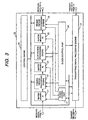
- FIG. 3 shows the construction of the base band signal processing part 12 in the wireless communication apparatus according to one embodiment of the present invention.
- the present embodiment shows the base band signal processing part which processes the signal of the frame structure mentioned in FIGS. 9A to 9C , and the base band signal processing part 12 comprises one large scale integrated (LSI) circuit.
- the received base band signal which is supplied from the radio frequency circuit 11 is stored in a buffer memory 21.
- the received signal stored in the buffer memory 21 is subjected to a synchronizing process and a spectrum despreading process, etc. by a symbol period processing engine 22, thereby converting the signal into a signal based on a symbol unit.
- the signal based on the symbol unit is stored in a buffer memory 23.
- a slot period processing engine 24 performs processes such as detection and Rake combining, and stores the signals in a buffer memory 25.
- a frame period processing engine 26 performs processes such as de-interleave and error correction, and outputs the signals as received data to the data processing part 13.
- transmitting data to be supplied from the data processing part 13 is subjected to processes such as error correction encoding, interleave, modulation, spectrum spread by a transmitting signal processing engine 29, and the processed transmitting-signal is outputted to the radio frequency circuit 11.
- the symbol period processing engine 22 and the slot period processing engine 24 as signal processing engines watch whether or not there is data to be processed by the slot period processing engine 24 and the frame period processing engine 26 as the individual subsequent signal processing engines.
- a control engine 20 controls operations of the symbol period processing engine 22, slot period processing engine 24, frame period processing engine 26, and transmitting signal processing engine 29 as the signal processing engines, thereby issuing an instruction to subsequently perform the above-mentioned signal processing.
- the control engine 20 supplies a clock signal only for a period in which the symbol period processing engine 22, slot period processing engine 24, frame period processing engine 26, and transmitting signal processing engine 29 are to be operated. For a period except therefor, the control engine 20 controls a clock control part 28 to suspend the clock signal. Also, based on the watched result, the control engine 20 controls a power source control part 27 to reduce power consumption for a period in which the symbol period processing engine 22, slot period processing engine 24, frame period processing engine 26, and transmitting signal processing engine 29, and the buffer memories 21, 23, and 25 are not operated. To be specific, the control engine 20 decreases a power voltage for a period in which the operation is unnecessary and generates a specific bias voltage to diminish a leak current of the memory, etc.
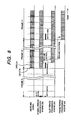
- FIG. 4 shows the construction of the symbol period processing engine 22 as the signal processing engine. Although FIG. 4 also shows the construction of the symbol period processing engine 22 and the buffer memories 21 and 23 on the input/output side thereof, the same construction as the foregoing is applied to that of the slot period processing engine 24 and the buffer memories 23 and 24 on the input/output side thereof and that of the frame period processing engine 26 and the buffer memory 25 on the input side thereof.
- the symbol period processing engine 22 as the signal processing engine reads out the signal stored in the buffer memory 21.
- the read-out signal is subjected to a signal process by a simplified processor 30 and an auxiliary hardware 31 for processing the read-out signal.
- the processed result is stored in the buffer memory 23.
- the signal processing engine 22 has an internal memory (RAM) 32 which stores parameters, etc. necessary for temporary storage of the processed result and operations.
- the simplified processor 30 d-controls the operation with the symbol period processing engine 22 in accordance with an instruction of the control engine 20, executes a signal process necessary for the symbol period processing engine 22 in collaboration with the auxiliary hardware 31, and transmits various measured results, watched result, and operating processing state to the control engine 20.
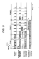
- FIG. 5 is a time chart showing an example of the operational sequence when no user data DPDCH is transmitted in the received signal in the wireless communication apparatus according to the embodiment of the present invention.
- horizontal-line portions, oblique-line portions, and vertical-line portions indicate that there is valid data.
- FIG. 5 indicates that in the received signals, there is valid data in the user data DPCCH and DPDCH in a frame 1 and, on the contrary, there is valid data only in the user data DPCCH and no valid data in the user data DPDCH in frames 2 and 3.
- the symbol period processing engine 22, slot period processing engine 24, and frame period processing engine 27 continuously operate.
- the symbol period processing engine 22 watches whether or not there is valid data in the user data DPDCH in the received signals in the slot portion at the head of the frame.
- the control engine 20 controls the clock control part 28 and the power source control part 27 so that the symbol period processing engine 22 operates only during one slot period at the head of the frame and during reception of the DPCCH data. Also, the control engine 20 controls the operation so that the slot period processing engine 24 operates only during one slot period at the head of the frame and during reception of the DPCCH. Further, the control engine 20 controls an operation to suspend so that the frame period processing engine 26 is suspended after the frame process which is currently being processed is finished. Thereafter, the symbol period processing engine 22 intermittently continues a process of the DPCCH while watching the resumption of the DPDCH data portion or the suspension of the DPCCH data portion in the head slots of the subsequent frames to frame 3.
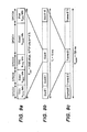
- FIG. 6 is a time chart showing an example of the operational sequence in the case of change from a state in which there is only the DPCCH data portion in the received signals to the frame in which the DPDCH resumes in the wireless communication apparatus according to the embodiment of the present invention.
- the symbol period processing engine 22 watches the resumption of the DPDCH data portion and the suspension of the DPCCH data portion in the slot at the head of the frame while processing the DPCCH data portion in a period (frame 4) in which there is not DPDCH data portion. As the watched result, if the resumption of the DPDCH data portion is detected as indicated in a frame 5, the symbol period processing engine 22 transmits the watched result to the control engine 20.
- the control engine 20 controls the clock control part 28 and the power source control part 27 so that, subsequently thereto, the symbol period processing engine 22 and the slot period processing engine 24 operate continuously. Also, the control engine 20 controls the resumption of operation of the frame period processing engine 26 (frame 6), thus executing a decoding process of the resumed user data. Subsequently thereto, the symbol period processing engine 22, slot period processing engine 24, and frame period processing engine 26 as the signal processing engines operate continuously for a period in which there is DPDCH data portion in the slot at the head of the frame.
- FIG. 7 is a time chart showing an example of the operational sequence in the case of change from a state in which there is only the DPCCH data portion in the received signals to the frame in which the DPCCH suspends in the wireless communication apparatus according to the embodiment of the present invention.
- the symbol period processing engine 22 watches the resumption of the DPDCH data portion and the suspension of the DPCCH data portion in the slot at the head of the frame while intermittently executing a process for the DPCCH data portion. As the watched result, if the suspension (non-existence) of the DPCCH data portion is detected at the head of the frame as indicated in a frame 8, the symbol period processing engine 22 transmits the watched result to the control engine 20.
- the control engine 20 controls the clock control part 28 and the power source control part 27 based on the watched result so that, subsequently thereto, the symbol period processing engine 22 operates only during the period of the DPCCH data portion at the head of the frame and the slot period processing engine 24 suspends the operation subsequent to the next slot. After that, the symbol period processing engine 22 operates only for a period of the DPCCH data portion in the slot at the head of the frame and watches the resumption of the DPCCH data portion as indicated in a frame 9.
- FIG. 8 is a time chart showing an example of the operational sequence in the case of change from a state in which the received signal is completely suspended to a state in which the DPCCH and DPDCH data portions resume in the wireless communication apparatus according to the embodiment of the present invention.
- the symbol period processing engine 22 operates for the period of the DPCCH data portion in the slot at the head of the frame and watches the resumption of the DPCCH data portion.
- the control engine 20 controls the clock control part 28 and the power source control part 27 so that, subsequently thereto, the symbol period processing engine 22 operates for a period over the frame 10, the slot period processing engine 24 continuously operates for a period of slots subsequent to the second slot in the frame 10, and the frame period processing engine 26 continuously operates for a period of data subsequent to a frame 11.
- a decoding process of the resumed user data is performed. After that, the symbol period processing engine 22, slot period processing engine 24, and frame period processing engine 26 continuously operate.
- the number of operating signal processing circuits can be minimized in the intermittent transmitting sequence of the packet data which is prescribed in FIG. 10 , thereby effectively reducing power consumption.
- the present invention is not limited to the above embodiment and can be embodied to a wireless communication apparatus for intermittently communicating data. It is unnecessary to control clock signals and power sources of all plural signal processing blocks having different processing functions, and it is possible to control the clock signal and power source of the main signal processing block.
Claims (10)
- Partie de traitement de signal en bande de base (12, 13) pour traiter un signal incluant des données intermittentes dans un dispositif de communication sans fil, comportant :un premier bloc de traitement de signal (22, 24) pour traiter périodiquement un signal,un second bloc de traitement de signal (24, 26) pour traiter périodiquement, avec une période de traitement plus longue que ledit premier bloc de traitement (22, 24), un signal traité par ledit premier bloc de traitement de signal (22, 24),une mémoire tampon (23, 25) entre lesdits premier et second blocs de traitement de signal (22, 24, 26),une partie de commande d'horloge (28) pour délivrer un signal d'horloge auxdits blocs de traitement de signal (22, 24, 26) et à ladite mémoire tampon (23, 25),une partie de commande de source d'alimentation (27) pour délivrer de l'énergie à chacun desdits blocs de traitement de signal (22, 24, 26) et à ladite mémoire tampon (23, 25), etun moteur de commande (20) pour commander lesdits blocs de traitement de signal, ladite mémoire tampon, ladite partie de commande d'horloge et ladite partie de commande de source d'alimentation, etdans laquelle ledit premier bloc de traitement de signal (22, 24) inclut des moyens d'observation pour observer un signal qui a été traité et déterminer si ledit signal doit être en plus traité dans le second bloc de traitement de signal (24, 26), etdans laquelle ledit moteur de commande (20) est adapté pour commander également ladite partie de commande d'horloge (28) pour envoyer le signal d'horloge, ou suspendre l'envoi de celui-ci, audit second bloc de traitement de signal (24, 26) sur la base du résultat de la détermination par lesdits moyens d'observation.
- Dispositif de communication sans fil ayant une partie de traitement sans fil (11) pour traiter un signal sans fil incluant des données intermittentes, et une partie de traitement de signal en bande de base (12, 13) conformément à la revendication 1, pour recevoir lesdites données intermittentes en provenance de ladite partie de traitement sans fil.
- Dispositif de communication sans fil selon la revendication 2, dans lequel ledit moteur de commande (20) est en outre adapté pour commander ladite partie de commande de source d'alimentation (27) afin de délivrer de l'énergie audit second bloc de traitement de signal (24, 26) sur la base dudit résultat observé.
- Dispositif de communication sans fil selon la revendication 2, dans lequel lesdites données intermittentes comportent un signal ayant un format de signal incluant une partie de données de commande périodique et une partie de données utilisateur, et comportent un signal de commande périodique lorsqu'il n'y a pas ladite partie de données utilisateur, et
ledit premier bloc de traitement de signal est adapté pour observer l'existence de ladite partie de données utilisateur et ledit moteur de commande (20) est adapté pour commander ladite partie de commande d'horloge afin d'envoyer le signal d'horloge ou de suspendre l'envoi de celui-ci audit second bloc de traitement de signal sur une période au cours de laquelle ladite partie de données utilisateur aurait dû être traitée, selon qu'il y ait ladite partie de données utilisateur conformément au résultat d'observation. - Dispositif de communication sans fil selon la revendication 4, dans lequel ledit moteur de commande (20) a en outre des moyens pour commander ladite partie de commande de source d'alimentation (27) afin de commander l'énergie délivrée audit second bloc de traitement de signal (24, 26) sur la base dudit résultat observé.
- Dispositif de communication sans fil selon la revendication 2, dans lequel lesdites données intermittentes comportent un signal ayant un format de signal incluant une partie de données de commande périodique et une partie de données utilisateur, et comportent un signal de commande périodique lorsqu'il n'y a pas ladite partie de données utilisateur, mais avec ladite partie de données de commande périodique suspendue lorsqu'il n'y a pas ladite partie de données utilisateur séquentiellement un nombre de fois prédéterminés ou supérieur, et
ledit moteur de commande (20) étant adapté pour commander ladite partie de commande d'horloge (28) afin d'envoyer le signal d'horloge, ou de suspendre l'envoi de celui-ci, audit second bloc de traitement de signal (24, 26) pendant une période au cours de laquelle le signal de commande doit être traité sur la base dudit résultat observé. - Dispositif de communication sans fil selon la revendication 6, dans lequel ledit moteur de commande (20) est en outre adapté pour commander ladite partie de commande de source d'alimentation (27) afin de commander l'énergie délivrée audit second bloc de traitement de signal (24, 26) sur la base dudit résultat observé.
- Partie de traitement de signal en bande de base selon la revendication 1, comportant un circuit intégré à grande échelle, laquelle comporte :ledit premier bloc de traitement de signal (22, 24),ledit second bloc de traitement de signal (24, 26),ladite mémoire tampon (23, 25),ladite partie de commande d'horloge (28),ladite partie de commande de source d'alimentation (27), etledit moteur de commande (20).
- Partie de traitement de signal en bande de base selon la revendication 8, dans laquelle lesdits blocs de traitement de signal (22, 24, 26) comportent : un bloc de traitement de signal (22) pour traiter des données sur la base d'une unité de symbole, un bloc de traitement de signal (24) pour traiter des données sur la base d'une unité d'intervalle de temps, et un bloc de traitement de signal (26) pour traiter des données sur la base d'une unité de trame.
- Partie de traitement de signal en bande de base selon la revendication 1, dans laquelle ledit moteur de commande (20) est adapté pour suspendre l'envoi du signal d'horloge audit second bloc de traitement de signal (24, 26) lorsque lesdits moyens d'observation détectent que ledit premier bloc de traitement de signal (22, 24) a arrêté le traitement d'un signal qui devait être en plus traité dans ledit second bloc de traitement de signal (24, 26).
Applications Claiming Priority (2)
| Application Number | Priority Date | Filing Date | Title |
|---|---|---|---|
| JP2001033392A JP3819242B2 (ja) | 2001-02-09 | 2001-02-09 | 断続信号を扱う無線通信装置 |
| JP2001033392 | 2001-02-09 |
Publications (3)
| Publication Number | Publication Date |
|---|---|
| EP1231801A2 EP1231801A2 (fr) | 2002-08-14 |
| EP1231801A3 EP1231801A3 (fr) | 2003-08-27 |
| EP1231801B1 true EP1231801B1 (fr) | 2009-12-30 |
Family
ID=18897148
Family Applications (1)
| Application Number | Title | Priority Date | Filing Date |
|---|---|---|---|
| EP20010113086 Expired - Lifetime EP1231801B1 (fr) | 2001-02-09 | 2001-05-29 | Appareil de communication sans fil à traitement de données intermittent |
Country Status (6)
| Country | Link |
|---|---|
| US (1) | US6807235B2 (fr) |
| EP (1) | EP1231801B1 (fr) |
| JP (1) | JP3819242B2 (fr) |
| KR (1) | KR100730258B1 (fr) |
| DE (1) | DE60140930D1 (fr) |
| TW (1) | TW561731B (fr) |
Families Citing this family (30)
| Publication number | Priority date | Publication date | Assignee | Title |
|---|---|---|---|---|
| US6993669B2 (en) * | 2001-04-18 | 2006-01-31 | Gallitzin Allegheny Llc | Low power clocking systems and methods |
| US6990598B2 (en) * | 2001-03-21 | 2006-01-24 | Gallitzin Allegheny Llc | Low power reconfigurable systems and methods |
| KR100402786B1 (ko) * | 2001-07-30 | 2003-10-22 | 한국전자통신연구원 | 무선 통신 단말기에서의 전송율 정보 매핑 장치 및 그 방법 |
| US7502817B2 (en) * | 2001-10-26 | 2009-03-10 | Qualcomm Incorporated | Method and apparatus for partitioning memory in a telecommunication device |
| US7269448B2 (en) * | 2001-11-09 | 2007-09-11 | Electronics And Telecommunications Research Institute | Method for recognizing request for data transmission by mobile/base station RRC using network transfer device |
| US6907028B2 (en) * | 2002-02-14 | 2005-06-14 | Nokia Corporation | Clock-based time slicing |
| US7130313B2 (en) | 2002-02-14 | 2006-10-31 | Nokia Corporation | Time-slice signaling for broadband digital broadcasting |
| EP1511221B1 (fr) * | 2003-03-27 | 2020-05-20 | Optis Wireless Technology, LLC | Procede et dispositif de communication intermittente |
| US7478260B2 (en) * | 2003-10-20 | 2009-01-13 | Hewlett-Packard Development Company, L.P. | System and method for setting a clock rate in a memory card |
| US9112620B2 (en) * | 2005-03-10 | 2015-08-18 | Qualcomm Incorporated | Method of enabling power savings when no data is being transmitted on a media logical channel |
| US20060259807A1 (en) * | 2005-05-10 | 2006-11-16 | Telairity Semiconductor, Inc. | Method and apparatus for clock synchronization between a processor and external devices |
| JP4513974B2 (ja) * | 2005-06-27 | 2010-07-28 | 日本電気株式会社 | 優先度の高い情報を同報する無線通信ネットワーク、その変更方法、及び無線通信ネットワーク設計ツール |
| JP2007095040A (ja) * | 2005-08-31 | 2007-04-12 | Matsushita Electric Ind Co Ltd | データ処理装置、プログラム、記録媒体、コンテンツ再生装置 |
| US20070124395A1 (en) * | 2005-09-22 | 2007-05-31 | Stephen Edge | Geography-based filtering of broadcasts |
| JP4509945B2 (ja) * | 2006-02-08 | 2010-07-21 | 富士通株式会社 | データ転送装置におけるデバイスの発熱制御装置 |
| TWI316374B (en) * | 2006-07-21 | 2009-10-21 | Hon Hai Prec Ind Co Ltd | System and method for saving power of station |
| US7620833B2 (en) * | 2006-12-04 | 2009-11-17 | Intel Corporation | Power saving for isochronous data streams in a computer system |
| US7916676B2 (en) * | 2007-03-23 | 2011-03-29 | Broadcom Corporation | Method and system for holistic energy management in ethernet networks |
| US8849183B2 (en) | 2007-10-05 | 2014-09-30 | Qualcomm Incorporated | Location and time based filtering of broadcast information |
| JP4962396B2 (ja) * | 2008-04-23 | 2012-06-27 | 日本電気株式会社 | パケット処理装置 |
| JP5007703B2 (ja) * | 2008-05-19 | 2012-08-22 | 日本電気株式会社 | パケット処理装置、パケット制御方法及びパケット制御プログラム |
| US9280778B2 (en) | 2008-12-15 | 2016-03-08 | Qualcomm Incorporated | Location logging and location and time based filtering |
| US8374091B2 (en) * | 2009-03-26 | 2013-02-12 | Empire Technology Development Llc | TCP extension and variants for handling heterogeneous applications |
| CN103003769B (zh) * | 2010-07-20 | 2016-02-24 | 飞思卡尔半导体公司 | 时钟电路、电子设备以及提供时钟信号的方法 |
| KR20120018266A (ko) * | 2010-08-20 | 2012-03-02 | 삼성전자주식회사 | 직교 주파수 분할 다중 접속 방법을 사용하는 무선 통신 시스템에서 기지국의 전력 증폭기 소모 전력 제어 방법 및 장치 |
| US9485108B2 (en) | 2011-03-14 | 2016-11-01 | Qualcomm Incorporated | System and apparatus for using multichannel file delivery over unidirectional transport (“FLUTE”) protocol for delivering different classes of files in a broadcast network |
| US9451401B2 (en) | 2011-05-27 | 2016-09-20 | Qualcomm Incorporated | Application transport level location filtering of internet protocol multicast content delivery |
| KR200457848Y1 (ko) * | 2011-08-19 | 2012-01-05 | 이호상 | 의료용 침대 |
| US9310873B2 (en) * | 2012-08-31 | 2016-04-12 | Vixs Systems, Inc. | Video processing device with register adjustment generator and methods for use therewith |
| US11463095B2 (en) | 2018-09-26 | 2022-10-04 | Apple Inc. | Frequency generation and synchronization systems and methods |
Family Cites Families (6)
| Publication number | Priority date | Publication date | Assignee | Title |
|---|---|---|---|---|
| JPH01190054A (ja) | 1988-01-25 | 1989-07-31 | Man Design Kk | 受信機 |
| FI97765C (fi) | 1993-11-26 | 1997-02-10 | Nokia Mobile Phones Ltd | Menetelmä sekä kytkentäjärjestely kutsuviestien käsittelemiseksi matkaviestimessä |
| EP1083665B1 (fr) | 1994-07-21 | 2008-02-06 | Interdigital Technology Corporation | Procedé et appareil pour diminuer la consommation de courant dans une unite d'abonne d'un système de telecommunication |
| ATE205616T1 (de) * | 1994-10-19 | 2001-09-15 | Advanced Micro Devices Inc | Integrierte prozessorsysteme für tragbare informationsgeräte |
| US6647502B1 (en) * | 1999-07-13 | 2003-11-11 | Sony Corporation | Method and apparatus for providing power based on the amount of data stored in buffers |
| US6691071B2 (en) * | 2002-05-13 | 2004-02-10 | Motorola, Inc. | Synchronizing clock enablement in an electronic device |
-
2001
- 2001-02-09 JP JP2001033392A patent/JP3819242B2/ja not_active Expired - Fee Related
- 2001-03-01 US US09/795,110 patent/US6807235B2/en not_active Expired - Fee Related
- 2001-05-09 TW TW90111055A patent/TW561731B/zh not_active IP Right Cessation
- 2001-05-29 DE DE60140930T patent/DE60140930D1/de not_active Expired - Lifetime
- 2001-05-29 EP EP20010113086 patent/EP1231801B1/fr not_active Expired - Lifetime
- 2001-08-31 KR KR20010053168A patent/KR100730258B1/ko not_active IP Right Cessation
Also Published As
| Publication number | Publication date |
|---|---|
| JP2002237760A (ja) | 2002-08-23 |
| KR20020066166A (ko) | 2002-08-14 |
| EP1231801A3 (fr) | 2003-08-27 |
| TW561731B (en) | 2003-11-11 |
| DE60140930D1 (de) | 2010-02-11 |
| KR100730258B1 (ko) | 2007-06-20 |
| EP1231801A2 (fr) | 2002-08-14 |
| JP3819242B2 (ja) | 2006-09-06 |
| US6807235B2 (en) | 2004-10-19 |
| US20020111199A1 (en) | 2002-08-15 |
Similar Documents
| Publication | Publication Date | Title |
|---|---|---|
| EP1231801B1 (fr) | Appareil de communication sans fil à traitement de données intermittent | |
| KR100576680B1 (ko) | 스펙트럼 확산 신호를 전송하기 위한 전송기를 구비하는 통신시스템에 사용되는 수신기 | |
| EP0829967B1 (fr) | Radioémetteur-récepteur à AMRT avec un circuit économiseur d'énergie | |
| US7142896B2 (en) | Method and apparatus for reducing power consumption of slotted mode mobile communication terminal | |
| US20060092886A1 (en) | CDMA communication system and its transmission power control method | |
| AU748389B2 (en) | Power saving method and apparatus for radio base station | |
| GB2354911A (en) | Method of reducing power consumption of a communicaton device | |
| US8396504B2 (en) | Mobile terminal device and control method for saving electric power of mobile terminal device | |
| KR100350474B1 (ko) | 디지털 무선 통신 단말 시스템에서 대기시 적응적 전력소모 감소 방법 | |
| US7062285B2 (en) | Reliable decoding of quick paging channel in IS2000 handsets | |
| US20030086383A1 (en) | Current reduction by receiver linearity adjustment in a communication device | |
| JP2005175731A (ja) | Agc制御システム及びその制御方法並びにそれを用いた受信機 | |
| JP4223773B2 (ja) | 無線通信端末 | |
| US20050227743A1 (en) | Method and device for receiving radio signal | |
| JP2004236350A (ja) | 断続信号を扱う無線通信装置 | |
| JP4870321B2 (ja) | 不連続データ送信中に回路素子の電源断により生じるローカル搬送波信号中の位相雑音を減少させる装置 | |
| JP2005110179A (ja) | 受信装置、送受信装置及びその装置の制御方法 | |
| WO1999016190A1 (fr) | Equipement et procede pour communication radio | |
| KR100208003B1 (ko) | 디지털 무선 단말 시스템의 동작 흐름 제어 장치및 방법 | |
| JP3972042B2 (ja) | Cdma移動送信装置及びこれを用いた方法 | |
| JPWO2002047420A1 (ja) | 無線通信方法および装置 | |
| JP2004194166A (ja) | 送信電力制御システム | |
| KR20040108273A (ko) | 이동 통신 단말기의 페이징 주기 설정 방법 |
Legal Events
| Date | Code | Title | Description |
|---|---|---|---|
| PUAI | Public reference made under article 153(3) epc to a published international application that has entered the european phase |
Free format text: ORIGINAL CODE: 0009012 |
|
| AK | Designated contracting states |
Kind code of ref document: A2 Designated state(s): AT BE CH CY DE DK ES FI FR GB GR IE IT LI LU MC NL PT SE TR |
|
| AX | Request for extension of the european patent |
Free format text: AL;LT;LV;MK;RO;SI |
|
| PUAL | Search report despatched |
Free format text: ORIGINAL CODE: 0009013 |
|
| AK | Designated contracting states |
Designated state(s): AT BE CH CY DE DK ES FI FR GB GR IE IT LI LU MC NL PT SE TR |
|
| AX | Request for extension of the european patent |
Extension state: AL LT LV MK RO SI |
|
| 17P | Request for examination filed |
Effective date: 20040224 |
|
| AKX | Designation fees paid |
Designated state(s): DE FI FR GB SE |
|
| 17Q | First examination report despatched |
Effective date: 20040505 |
|
| GRAP | Despatch of communication of intention to grant a patent |
Free format text: ORIGINAL CODE: EPIDOSNIGR1 |
|
| RIC1 | Information provided on ipc code assigned before grant |
Ipc: H04W 52/02 20090101AFI20090623BHEP |
|
| GRAS | Grant fee paid |
Free format text: ORIGINAL CODE: EPIDOSNIGR3 |
|
| GRAA | (expected) grant |
Free format text: ORIGINAL CODE: 0009210 |
|
| AK | Designated contracting states |
Kind code of ref document: B1 Designated state(s): DE FI FR GB SE |
|
| REG | Reference to a national code |
Ref country code: GB Ref legal event code: FG4D |
|
| REF | Corresponds to: |
Ref document number: 60140930 Country of ref document: DE Date of ref document: 20100211 Kind code of ref document: P |
|
| PG25 | Lapsed in a contracting state [announced via postgrant information from national office to epo] |
Ref country code: SE Free format text: LAPSE BECAUSE OF FAILURE TO SUBMIT A TRANSLATION OF THE DESCRIPTION OR TO PAY THE FEE WITHIN THE PRESCRIBED TIME-LIMIT Effective date: 20091230 |
|
| PLBE | No opposition filed within time limit |
Free format text: ORIGINAL CODE: 0009261 |
|
| STAA | Information on the status of an ep patent application or granted ep patent |
Free format text: STATUS: NO OPPOSITION FILED WITHIN TIME LIMIT |
|
| 26N | No opposition filed |
Effective date: 20101001 |
|
| GBPC | Gb: european patent ceased through non-payment of renewal fee |
Effective date: 20100529 |
|
| PG25 | Lapsed in a contracting state [announced via postgrant information from national office to epo] |
Ref country code: GB Free format text: LAPSE BECAUSE OF NON-PAYMENT OF DUE FEES Effective date: 20100529 |
|
| REG | Reference to a national code |
Ref country code: DE Ref legal event code: R082 Ref document number: 60140930 Country of ref document: DE Representative=s name: STREHL, SCHUEBEL-HOPF & PARTNER, DE |
|
| REG | Reference to a national code |
Ref country code: DE Ref legal event code: R082 Ref document number: 60140930 Country of ref document: DE Representative=s name: STREHL SCHUEBEL-HOPF & PARTNER MBB PATENTANWAE, DE Effective date: 20120330 Ref country code: DE Ref legal event code: R081 Ref document number: 60140930 Country of ref document: DE Owner name: HITACHI CONSUMER ELECTRONICS CO., LTD., JP Free format text: FORMER OWNER: HITACHI, LTD., TOKYO, JP Effective date: 20120330 Ref country code: DE Ref legal event code: R082 Ref document number: 60140930 Country of ref document: DE Representative=s name: PATENTANWAELTE STREHL, SCHUEBEL-HOPF & PARTNER, DE Effective date: 20120330 Ref country code: DE Ref legal event code: R081 Ref document number: 60140930 Country of ref document: DE Owner name: HITACHI MAXELL, LTD., IBARAKI-SHI, JP Free format text: FORMER OWNER: HITACHI, LTD., TOKYO, JP Effective date: 20120330 |
|
| REG | Reference to a national code |
Ref country code: FR Ref legal event code: TP Owner name: HITACHI CONSUMER ELECTRONICS CO., LTD., JP Effective date: 20120510 |
|
| REG | Reference to a national code |
Ref country code: DE Ref legal event code: R082 Ref document number: 60140930 Country of ref document: DE Representative=s name: PATENTANWAELTE STREHL, SCHUEBEL-HOPF & PARTNER, DE |
|
| REG | Reference to a national code |
Ref country code: DE Ref legal event code: R082 Ref document number: 60140930 Country of ref document: DE Representative=s name: STREHL SCHUEBEL-HOPF & PARTNER MBB PATENTANWAE, DE Effective date: 20150317 Ref country code: DE Ref legal event code: R081 Ref document number: 60140930 Country of ref document: DE Owner name: HITACHI MAXELL, LTD., IBARAKI-SHI, JP Free format text: FORMER OWNER: HITACHI CONSUMER ELECTRONICS CO., LTD., TOKIO/TOKYO, JP Effective date: 20150317 Ref country code: DE Ref legal event code: R082 Ref document number: 60140930 Country of ref document: DE Representative=s name: PATENTANWAELTE STREHL, SCHUEBEL-HOPF & PARTNER, DE Effective date: 20150317 |
|
| REG | Reference to a national code |
Ref country code: FR Ref legal event code: PLFP Year of fee payment: 15 |
|
| REG | Reference to a national code |
Ref country code: FR Ref legal event code: TP Owner name: HITACHI MAXELL LTD., JP Effective date: 20150504 |
|
| PGFP | Annual fee paid to national office [announced via postgrant information from national office to epo] |
Ref country code: DE Payment date: 20150527 Year of fee payment: 15 Ref country code: FI Payment date: 20150512 Year of fee payment: 15 |
|
| PGFP | Annual fee paid to national office [announced via postgrant information from national office to epo] |
Ref country code: FR Payment date: 20150508 Year of fee payment: 15 |
|
| REG | Reference to a national code |
Ref country code: DE Ref legal event code: R119 Ref document number: 60140930 Country of ref document: DE |
|
| PG25 | Lapsed in a contracting state [announced via postgrant information from national office to epo] |
Ref country code: FI Free format text: LAPSE BECAUSE OF NON-PAYMENT OF DUE FEES Effective date: 20160529 |
|
| REG | Reference to a national code |
Ref country code: FR Ref legal event code: ST Effective date: 20170131 |
|
| PG25 | Lapsed in a contracting state [announced via postgrant information from national office to epo] |
Ref country code: DE Free format text: LAPSE BECAUSE OF NON-PAYMENT OF DUE FEES Effective date: 20161201 Ref country code: FR Free format text: LAPSE BECAUSE OF NON-PAYMENT OF DUE FEES Effective date: 20160531 |