EP1230780B1 - Anpassbare chipkarte - Google Patents
Anpassbare chipkarte Download PDFInfo
- Publication number
- EP1230780B1 EP1230780B1 EP99974203A EP99974203A EP1230780B1 EP 1230780 B1 EP1230780 B1 EP 1230780B1 EP 99974203 A EP99974203 A EP 99974203A EP 99974203 A EP99974203 A EP 99974203A EP 1230780 B1 EP1230780 B1 EP 1230780B1
- Authority
- EP
- European Patent Office
- Prior art keywords
- chip card
- data unit
- apdu
- eeprom
- card according
- Prior art date
- Legal status (The legal status is an assumption and is not a legal conclusion. Google has not performed a legal analysis and makes no representation as to the accuracy of the status listed.)
- Revoked
Links
Images


Classifications
-
- H—ELECTRICITY
- H04—ELECTRIC COMMUNICATION TECHNIQUE
- H04W—WIRELESS COMMUNICATION NETWORKS
- H04W24/00—Supervisory, monitoring or testing arrangements
-
- G—PHYSICS
- G06—COMPUTING OR CALCULATING; COUNTING
- G06K—GRAPHICAL DATA READING; PRESENTATION OF DATA; RECORD CARRIERS; HANDLING RECORD CARRIERS
- G06K19/00—Record carriers for use with machines and with at least a part designed to carry digital markings
- G06K19/06—Record carriers for use with machines and with at least a part designed to carry digital markings characterised by the kind of the digital marking, e.g. shape, nature, code
- G06K19/067—Record carriers with conductive marks, printed circuits or semiconductor circuit elements, e.g. credit or identity cards also with resonating or responding marks without active components
- G06K19/07—Record carriers with conductive marks, printed circuits or semiconductor circuit elements, e.g. credit or identity cards also with resonating or responding marks without active components with integrated circuit chips
- G06K19/0719—Record carriers with conductive marks, printed circuits or semiconductor circuit elements, e.g. credit or identity cards also with resonating or responding marks without active components with integrated circuit chips at least one of the integrated circuit chips comprising an arrangement for application selection, e.g. an acceleration sensor or a set of radio buttons
-
- G—PHYSICS
- G06—COMPUTING OR CALCULATING; COUNTING
- G06K—GRAPHICAL DATA READING; PRESENTATION OF DATA; RECORD CARRIERS; HANDLING RECORD CARRIERS
- G06K19/00—Record carriers for use with machines and with at least a part designed to carry digital markings
- G06K19/06—Record carriers for use with machines and with at least a part designed to carry digital markings characterised by the kind of the digital marking, e.g. shape, nature, code
- G06K19/067—Record carriers with conductive marks, printed circuits or semiconductor circuit elements, e.g. credit or identity cards also with resonating or responding marks without active components
- G06K19/07—Record carriers with conductive marks, printed circuits or semiconductor circuit elements, e.g. credit or identity cards also with resonating or responding marks without active components with integrated circuit chips
- G06K19/073—Special arrangements for circuits, e.g. for protecting identification code in memory
-
- G—PHYSICS
- G06—COMPUTING OR CALCULATING; COUNTING
- G06K—GRAPHICAL DATA READING; PRESENTATION OF DATA; RECORD CARRIERS; HANDLING RECORD CARRIERS
- G06K7/00—Methods or arrangements for sensing record carriers, e.g. for reading patterns
- G06K7/0095—Testing the sensing arrangement, e.g. testing if a magnetic card reader, bar code reader, RFID interrogator or smart card reader functions properly
-
- G—PHYSICS
- G06—COMPUTING OR CALCULATING; COUNTING
- G06Q—INFORMATION AND COMMUNICATION TECHNOLOGY [ICT] SPECIALLY ADAPTED FOR ADMINISTRATIVE, COMMERCIAL, FINANCIAL, MANAGERIAL OR SUPERVISORY PURPOSES; SYSTEMS OR METHODS SPECIALLY ADAPTED FOR ADMINISTRATIVE, COMMERCIAL, FINANCIAL, MANAGERIAL OR SUPERVISORY PURPOSES, NOT OTHERWISE PROVIDED FOR
- G06Q20/00—Payment architectures, schemes or protocols
- G06Q20/30—Payment architectures, schemes or protocols characterised by the use of specific devices or networks
- G06Q20/34—Payment architectures, schemes or protocols characterised by the use of specific devices or networks using cards, e.g. integrated circuit [IC] cards or magnetic cards
- G06Q20/355—Personalisation of cards for use
- G06Q20/3552—Downloading or loading of personalisation data
-
- G—PHYSICS
- G07—CHECKING-DEVICES
- G07F—COIN-FREED OR LIKE APPARATUS
- G07F7/00—Mechanisms actuated by objects other than coins to free or to actuate vending, hiring, coin or paper currency dispensing or refunding apparatus
- G07F7/08—Mechanisms actuated by objects other than coins to free or to actuate vending, hiring, coin or paper currency dispensing or refunding apparatus by coded identity card or credit card or other personal identification means
- G07F7/10—Mechanisms actuated by objects other than coins to free or to actuate vending, hiring, coin or paper currency dispensing or refunding apparatus by coded identity card or credit card or other personal identification means together with a coded signal, e.g. in the form of personal identification information, like personal identification number [PIN] or biometric data
- G07F7/1008—Active credit-cards provided with means to personalise their use, e.g. with PIN-introduction/comparison system
-
- H—ELECTRICITY
- H04—ELECTRIC COMMUNICATION TECHNIQUE
- H04L—TRANSMISSION OF DIGITAL INFORMATION, e.g. TELEGRAPHIC COMMUNICATION
- H04L9/00—Cryptographic mechanisms or cryptographic arrangements for secret or secure communications; Network security protocols
- H04L9/40—Network security protocols
-
- H—ELECTRICITY
- H04—ELECTRIC COMMUNICATION TECHNIQUE
- H04W—WIRELESS COMMUNICATION NETWORKS
- H04W12/00—Security arrangements; Authentication; Protecting privacy or anonymity
- H04W12/40—Security arrangements using identity modules
Definitions
- the present invention relates to a chip card, in particular a smart card, adapted to its manufacture and distribution can be.
- Smart cards communicate with external devices, for example, with a mobile phone, via a logical interface, the Often referred to as API (Application Protocol Interface). If the external device wants to access a functionality of the smart card, It sends a command via this API interface. The card, the one Get command from external device, can decode it and one trigger appropriate action.
- API Application Protocol Interface
- Such commands are usually structured data units which is called APDU (Application Packet Data Unit).
- An APDU usually consists of a header and a content part ("Body"), where the intent of the instruction to be executed and the Specifies instruction parameters and the (not always available) content part Contains data.
- This protocol is inter alia in the ISO standard ISO / IEC 7816, part 4 described. Further commands are in the specifying system-specific documents (e.g., GSM 11.11, GSM 11.14).
- API interface and the standardization of APDU understood by smart cards, is usually in Standardization committees or is proposed by individual companies. For compatibility reasons between chip cards and devices of different manufacturers is a strong international standardization of API interface a desirable goal.
- WO9819237 (Schlumberger) describes a chip card with a Java virtual machine in which different applications in one EEPROM are stored. Applications can thus be changed or replaced become.
- the instructions handler is stored in ROM, so that No new instructions were added to the existing instruction set can be.
- APDU handler in the chip card, which determines the response to incoming data units to each Changed, for example supplemented, renewed or replaced, to redefined, proprietary or non-standard APDU too consider.
- a smart card which serves as an identification module in one digital cellular mobile phone is used, for example, a SIM card (Subscriber Identification Module) or a WIM card (Wireless Application Protocol Identification Module), or WIM / SM (SIM with WIM Application), for example, in a GSM (Global System for Mobile Telecommunication), WAP (Wireless Application Protocol) or UMTS mobile phone can be used.
- SIM card Subscriber Identification Module
- WIM / SM SIM with WIM Application
- GSM Global System for Mobile Telecommunication
- WAP Wireless Application Protocol
- UMTS mobile phone for example, in a GSM (Global System for Mobile Telecommunication), WAP (Wireless Application Protocol) or UMTS mobile phone can be used.
- JAVA card trademark of SUN Microsystems
- OpenCard cards can be applied.
- FIG. 1 schematically shows a known one conventional system.
- the system comprises a terminal 3 (Mobile Equipment ME) and a conventional SIM or WIM card 5.
- One Application for example a browser or an application program, For example, a program from a service provider will not illustrated data processing means in the mobile device 3 executed.
- the Application communicates with the mobile device 3 via an API interface 2 (Application Protocol Interface) which is not detailed here.
- the mobile device 3 communicates with the SIM card 5 via a other API interface 4.
- the mobile device 3 usually handles the Role of the master of communication over this interface while the SIM card 5 answers as a slave.
- protocol variants known for example, according to SIM Toolkit, ie GSM 11.14, in which the SIM card at least temporarily assumes the role of the master.
- a step in the API protocol consists of sending a Command to the smart card 5, from the execution of the command by the card and optionally from the transmission of a response to the mobile device 3. Via the interface 4, therefore, either commands or responses replaced. Data can be both in the commands and / or in the Answers may be included.
- APDU Application Protocol Data Unit
- Additional APDU were for SIM cards and for WIM maps defined to the functionality of the API interface 4 too expand.
- FIG. 2 shows the typical structure of a data unit (APDU) 20.
- the data unit contains a mandatory header 200 with four bytes and a not always present content part (Body) 201 with a variable length.
- Body content part
- the header contains a first byte (CLA) that is used to indicate, among other things, which API version the data unit follows.
- a second byte (INS) indicates the instruction issued by the chip card 5 has to be executed or has just been executed. Depending on Instructions can be given two more parameters P1 and P2. If an instruction does not require a parameter P1 and / or P2, then this parameter will be set to zero.
- the optional content part 201 contains data and at least one Byte, which is the length of this data and / or the maximum length of the expected answer indicates.
- the conventional smart card 5 generally comprises a ROM 50, an EEPROM 51 and a RAM 52, and data processing means, not shown.
- the ROM is typically 64 today Kilobytes and usually contains the operating system, a Java virtual Machine (JVM, trademark of SUN), and various components F1, F2, .., for example JavaBeans, applets or programs that various functions of the card can offer.
- JVM Java virtual Machine
- EEPROM 51 Components are also stored, such as components as Applet after the personalization of the card were downloaded as well personal data of the user, for example, a telephone directory, a electronic certificate, etc.
- the EEPROM can be for example 16 or 32 Kilobytes include.
- RAM 52 stores temporary data for example, temporary variables. Next in the EEPROM ft Applications (applets) are saved.
- a data unit machine 500 receives the APDU of the mobile device 3 which via the API interface. 4 received and analyzes the header 200, in particular the bytes CLA and INS to issue the command to the affected component F1, F2, .. which can execute the command to forward.
- the APDU Handler 500 can then receive the response of that component and that answer send via the API interface 4 to the mobile device 3.
- the APDU handler 500 is commonly used as a program in ROM part 50 implemented.
- the program is by the Data processing means executed when an incoming APDU is detected. But it is also possible the APDU handler as a circuit to realize.
- a problem with this configuration is that the mobile device 3 and the application to new functionalities of the card, the for example, by new components G1, G2, .. in the ROM, in the EEPROM or in RAM can not be accessed, as long as no APDU 20 is standardized for this functionality.
- already distributed smart cards 5 do not offer this functionality if they only have one conventional APDU handler 500, which later defined this APDU can not detect - even if the required component G1, G2, .. is included in the card. For these reasons, new ones Functionalities due to the continuous and rapid development of the Chip cards would be possible to spread only slowly.
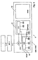
- FIG. 3 shows an example of a first variant of a Chip card 5 according to the invention, for example a SIM or WIM card, which can solve these problems.
- the chip card has a Test module 510, all received via the API interface 4 APDU 20 checks. If the test module detects that the received APDU was already provided in the production of the ROM part 50, it passes this APDU to a conventional APDU handler 500 in the ROM part 50, the corresponding functionality F1, F2, .. as described above for Provides.
- test module detects that the received APDU 20 in the preparation of the ROM 50 is not provided was, for example, because it was only in a later version of the API interface 4 has been standardized, it directs this APDU to a new Modified APDU handler 511 continues to be the one for this new APDU provided component G1, G2, G3, ... in the ROM or in the EEPROM retrieves.
- Module 510 contains a list of APDUs that conform to the conventional APDU Handler 500 should be routed and / or a list of newly defined APDU intended for the new APDU. This list is preferably also in the EEPROM and can thus be adapted become.
- the APDU handler 500 directs the received APDU to the new APDU handler 511 only if he received an error message from the conventional APDU handler namely, if the conventional APDU handler does not use this APDU can edit.
- test module 510 by the APDU determines to which APDU handler the received APDU 20 should be forwarded.
- the test module 510 by the APDU for example, by the byte CLA or INS itself determines to which APDU handler the received APDU 20 should be forwarded.
- APDUs that are routed to the new APDU handler 511 should be specially marked, for example by being misused, for example by being special, impossible or very unlikely Parameters P1, P2 or data 201 included.
- the new APDU handler 511 is preferably located in EEPROM 51. In this way he can also after the production of the ROMS 50 changed, for example, access to new, in the Meanwhile implemented components G1, G2, G3 to ensure.
- the test module 510 is also located in the EEPROM so that the Test conditions after the preparation of the ROM and / or after the Distribution of smart cards can be set. The test module 510 but could also be in ROM 50 or even in RAM 52.
- the new components G1, G2, G3, .. can be in ROM 50 or be included in the EEPROM 51. It can also temporarily in RAM 52 deposited components are provided. If the Chip card 5 at least temporarily the role of the master of the interface. 4 can also use this mechanism for functionalities, For example, access to applets from the mobile device 3 to Will be provided. It is even possible that the APDU handler 501 accesses components that are in an external device which, for example, via a contactless interface, For example, an infrared, RFID or Bluetooth interface, with the Mobile device 3 is connected.
- a contactless interface For example, an infrared, RFID or Bluetooth interface
- APDU Handler 500 in ROM part 50 modifies to automatically clear all Unrecognized received APDU to a new customizable APDU handler 511 in the EEPROM 51 forwards.
- This variant allows on the Test module 510 to renounce: what the conventional APDU handler 500 can not be edited automatically becomes the new APDU handler 511 transmitted.
- FIG. 4 shows a further variant of the invention Smart card. Same or comparable features are shown in all figures used with the same reference numerals and will not anymore described as long as this is not needed.
- the normal APDU handler usually located in the ROM 50 by replaced a modified APDU handler 512 in the EEPROM. In this way It can be customized at any time so that newly defined APDU can be considered.
- the modified APDU handlers also reside in RAM 52 so he can easily get through the Operating system of the chip card or changed by the application 1 can be.
- an application 1 to functionalities a smart card 5 access that in the production of the card is not yet and for which no APDU has been standardized, For example, on functionalities G1, G2, G3 .., which only at the Personalization or even after the distribution of the card over one Air interface as an applet were downloaded.
- test module 510 and / or the new one APDU Handler 511 or 512 with a message over a mobile network be adapted, for example with an SMS message, a USSD message, a GPRS packet, an IP packet, etc.
- the test module 510 and / or the APDU handler can also be used by an application 1, For example, a browser, which for example via the Air interface or loaded with a disk changed or supplemented.
- each APDU may perform of several different functions in the smart card 5 trigger.
- a special APDU defines what state the card is in and which set of functions must be used. These Variant allowed by sending a single APDU all Functionalities of the chip card replace by incoming APDU be edited by a new APDU handler. For example, you can in this way all parameters and components in the EEPROM 51 are temporarily replaced. Another special APDU can then return the smart card to its normal state.
Landscapes
- Engineering & Computer Science (AREA)
- Physics & Mathematics (AREA)
- General Physics & Mathematics (AREA)
- Computer Security & Cryptography (AREA)
- Computer Hardware Design (AREA)
- Microelectronics & Electronic Packaging (AREA)
- Theoretical Computer Science (AREA)
- Computer Networks & Wireless Communication (AREA)
- Signal Processing (AREA)
- Business, Economics & Management (AREA)
- Artificial Intelligence (AREA)
- Computer Vision & Pattern Recognition (AREA)
- General Engineering & Computer Science (AREA)
- Accounting & Taxation (AREA)
- Strategic Management (AREA)
- General Business, Economics & Management (AREA)
- Telephone Function (AREA)
- Stored Programmes (AREA)
- Photoreceptors In Electrophotography (AREA)
- Credit Cards Or The Like (AREA)
Description
Claims (20)
- Chipkarte (5), die über eine logische Schnittstelle (4) mit einer externen Vorrichtung (3) kommunizieren kann,
wobei standardisierte Dataeinheiten (20) für diese Kommunikation definiert sind,
wobei die Chipkarte über ein ROM und über ein EEPROM verfügt,
wobei verschiedene Komponenten (F1, F2, ..G1, G2..) vorgesehen sind, die verschiedene Funktionalitäten zur Verfügung stellen,
wobei ein Modul (500, 510, 511, 512) vorgesehen ist, um zu bestimmen, welche Komponente abgerufen wird, wenn eine bestimmte Dataeinheit (20) über die benannte logische Schnittstelle (4) empfangen wird,
dadurch gekennzeichnet, dass das benannte Modul mindestens teilweise im benannten EEPROM abgelegt ist. - Chipkarte gemäss dem vorhergehenden Anspruch, wobei das benannte Modul ein Test-Modul (510) umfasst, das derart ausgeführt ist, dass es bestimmte empfangene Dataeinheiten an einen konventionellen Application Packet Data Unit APDU-Handler (500) im ROM (50) und andere Dataeinheiten (20) an einen anderen APDU-Handler (511) weiterleiten kann.
- Chipkarte gemäss dem vorhergehenden Anspruch, in welchem das benannte Test-Modul (510) im ROM (50) abgelegt ist.
- Chipkarte gemäss dem Anspruch 2, in welchem das benannte Test-Modul (510) im EEPROM (51) abgelegt ist.
- Chipkarte gemäss einem der vorhergehenden Ansprüche, in welchem das benannte Test-Modul (510) derart ausgeführt ist, dass es anhand des Vorsatzes (200) der Dataeinheit (20) erkennen kann, wohin die Dataeinheit weitergeleitet werden soll.
- Chipkarte gemäss dem vorhergehenden Anspruch, in welchem der benannte Vorsatz mindestens folgende Bytes umfasst:wobei das benannte Test-Modul (510) derart ausgeführt ist, dass es anhand des benannten Parameters des Vorsatzes (200) der Dataeinheit (20) erkennen kann, wohin die Dataeinheit weitergeleitet werden soll.ein Byte (CLA), das die Klasse der Dataeinheit angibt,ein Byte, das die auszuführende Instruktion angibt,mindestens zwei Bytes, die mindestens zwei Parametern für die benannte auszuführende Instruktion entsprechen,
- Chipkarte gemäss dem Anspruch 5, in welchem der benannte Vorsatz mindestens folgende Bytes umfasst:wobei das benannte Test-Modul (510) derart ausgeführt ist, dass es anhand des benannten Parameters des Vorsatzes (200) der Dataeinheit (20) erkennen kann, wohin die Dataeinheit weitergeleitet werden soll.ein Byte (CLA), das die Klasse der Dataeinheit angibt,ein Byte, das die auszuführende Instruktion angibt,zwei Bytes, die zwei Parametern für die benannte auszuführende Instruktion entsprechen,
- Chipkarte gemäss einem der Ansprüche 1 bis 4, in welcher das benannte Test-Modul (510) derart ausgeführt ist, dass es anhand des Inhaltsteils (200) der Dataeinheit (20) erkennen kann, wohin die Dataeinheit weitergeleitet werden soll.
- Chipkarte gemäss dem Anspruch 1, die einen APDU-Handler (512) im EEPROM (51) umfasst, der derart ausgeführt ist, dass er alle empfangenen Dataeinheiten (20) an die zuständige Komponente (F1, G1, F2, G2, ..) in der benannten Chipkarte (5) weiterleiten kann.
- Chipkarte gemäss dem vorhergehenden Anspruch, in welchem der benannte APDU-Handler im EEPROM (51) abgelegt ist.
- Chipkarte gemäss dem Anspruch 9, in welchem der benannte APDU-Handler im RAM (52) abgelegt ist.
- Chipkarte gemäss dem Anspruch 1, die einen APDU-Handler (512) im ROM (50) umfasst, der derart ausgeführt ist, dass er alle unbekannten empfangenen Dataeinheiten (20) an einen zweiten APDU-Handler im EEPROM weiterleiten kann.
- Chipkarte gemäss einem der vorhergehenden Ansprüche, die eine SIM-Karte ist.
- Chipkarte gemäss dem vorhergehenden Anspruch, die eine WIM-Karte ist.
- Verfahren, um eine Chipkarte (5) nach Ihrer Herstellung an eine neue Standardisierung der API-Schnittstelle anzupassen, dadurch gekennzeichnet, dass im EEPROM (51) der Chipkarte ein Modul (510; 512) angepasst wird, welches bestimmt, welche Komponente abgerufen wird, wenn eine bestimmte Dataeinheit (20) über die benannte API Schnittstelle (4) empfangen wird.
- Verfahren gemäss dem vorhergehenden Anspruch, in welchem das benannte Modul (510; 512) im EEPROM mit einer Meldung über ein Mobilfunknetz angepasst wird.
- Verfahren gemäss dem vorhergehenden Anspruch, in welchem die benannte Meldung eine SMS-Meldung ist.
- Verfahren gemäss dem Anspruch 16, in welchem die benannte Meldung eine USSD-Meldung ist.
- Verfahren gemäss dem Anspruch 16, in welchem die benannte Meldung ein GPRS-Paket ist.
- Verfahren gemäss dem Anspruch 16, in welchem die benannte Meldung ein IP-Paket ist.
Applications Claiming Priority (1)
| Application Number | Priority Date | Filing Date | Title |
|---|---|---|---|
| PCT/CH1999/000553 WO2001039464A1 (de) | 1999-11-19 | 1999-11-19 | Anpassbare chipkarte |
Publications (2)
| Publication Number | Publication Date |
|---|---|
| EP1230780A1 EP1230780A1 (de) | 2002-08-14 |
| EP1230780B1 true EP1230780B1 (de) | 2005-03-09 |
Family
ID=4551739
Family Applications (1)
| Application Number | Title | Priority Date | Filing Date |
|---|---|---|---|
| EP99974203A Revoked EP1230780B1 (de) | 1999-11-19 | 1999-11-19 | Anpassbare chipkarte |
Country Status (6)
| Country | Link |
|---|---|
| US (2) | US6847831B2 (de) |
| EP (1) | EP1230780B1 (de) |
| AT (1) | ATE290744T1 (de) |
| AU (1) | AU1145800A (de) |
| DE (1) | DE59911743D1 (de) |
| WO (1) | WO2001039464A1 (de) |
Families Citing this family (13)
| Publication number | Priority date | Publication date | Assignee | Title |
|---|---|---|---|---|
| FR2793576B1 (fr) * | 1999-05-11 | 2001-11-16 | Gemplus Card Int | Terminal radiotelephonique avec une carte a puce dotee d'un navigateur |
| WO2001061659A1 (en) * | 2000-02-16 | 2001-08-23 | Mastercard International Incorporated | System and method for conducting electronic commerce with a remote wallet server |
| FR2846770B1 (fr) * | 2002-11-04 | 2005-01-28 | Oberthur Card Syst Sa | Carte a microcircuit comportant des moyens de publication de ses objets informatiques |
| JP2004172923A (ja) * | 2002-11-20 | 2004-06-17 | Nec Corp | 携帯電話端末及びそれに用いる有料サービス制限方法 |
| JP4158032B2 (ja) * | 2003-09-08 | 2008-10-01 | 日本電気株式会社 | 携帯電話機および間欠受信と定期的に行う必要のある処理との同期方法 |
| DE10342112A1 (de) * | 2003-09-10 | 2005-05-04 | Vodafone Holding Gmbh | Einrichtung zum Überprüfen einer SIM-Karte |
| US7324835B2 (en) * | 2004-08-07 | 2008-01-29 | C-One Technology Corporation | Motherboard and daughterboard multi-swap system with communication module for a GPRS system |
| EP1810535A1 (de) * | 2004-10-29 | 2007-07-25 | Telecom Italia S.p.A. | Verfahren zur herstellung einer sicheren logischen verbindung zwischen einer integrierten schaltungskarte und einer speicherkarte durch ein endgerät |
| DE102005019753A1 (de) * | 2005-04-28 | 2006-11-09 | Braun Gmbh | Blutdruckmessgerät sowie Chipkarte hierfür |
| DE602005024975D1 (de) * | 2005-10-31 | 2011-01-05 | Research In Motion Ltd | Kombinierte Batterie und Chipkarte |
| KR100735341B1 (ko) * | 2006-02-27 | 2007-07-04 | 삼성전자주식회사 | 가입자 식별 모듈의 데이터 리드 속도 개선 방법 및 장치 |
| EP2403275B1 (de) * | 2007-10-10 | 2016-07-06 | Morpho Cards GmbH | Telekommunikationschipkarte und Verfahren dafür |
| BRPI0722283A2 (pt) * | 2007-12-13 | 2014-04-15 | Nokia Corp | Método, aparelho, sistema, programa de computador, meio fisico e módulo |
Family Cites Families (12)
| Publication number | Priority date | Publication date | Assignee | Title |
|---|---|---|---|---|
| FI99071C (fi) * | 1995-02-15 | 1997-09-25 | Nokia Mobile Phones Ltd | Menetelmä sovellusten käyttämiseksi matkaviestimessä ja matkaviestin |
| US6385645B1 (en) * | 1995-08-04 | 2002-05-07 | Belle Gate Investments B.V. | Data exchange system comprising portable data processing units |
| FR2748834B1 (fr) * | 1996-05-17 | 1999-02-12 | Gemplus Card Int | Systeme de communication permettant une gestion securisee et independante d'une pluralite d'applications par chaque carte utilisateur, carte utilisateur et procede de gestion correspondants |
| GB2317246B (en) * | 1996-09-13 | 2001-08-08 | Orange Personal Comm Serv Ltd | Data store |
| PT932865E (pt) * | 1996-10-25 | 2002-12-31 | Schlumberger Systems & Service | Utilizacao de linguagem de programacao de nivel elevado com um microcontrolador |
| FI110399B (fi) * | 1997-06-19 | 2003-01-15 | Nokia Corp | Langaton viestin |
| WO2000025278A1 (en) * | 1998-10-27 | 2000-05-04 | Visa International Service Association | Delegated management of smart card applications |
| US6781957B2 (en) * | 1999-01-29 | 2004-08-24 | Avaya Technology Corp. | Application module interface for a control channel in a private branch exchange (PBX) environment |
| FR2790629A1 (fr) * | 1999-02-19 | 2000-09-08 | Bull Cp8 | Procede d'activation d'applications localisees dans une carte a puce par un navigateur du type dit "web" |
| US6725048B2 (en) * | 2000-09-22 | 2004-04-20 | Ericsson Inc. | Traffic congestion management when providing realtime information to service providers |
| US6824064B2 (en) * | 2000-12-06 | 2004-11-30 | Mobile-Mind, Inc. | Concurrent communication with multiple applications on a smart card |
| US7668315B2 (en) * | 2001-01-05 | 2010-02-23 | Qualcomm Incorporated | Local authentication of mobile subscribers outside their home systems |
-
1999
- 1999-11-19 EP EP99974203A patent/EP1230780B1/de not_active Revoked
- 1999-11-19 DE DE59911743T patent/DE59911743D1/de not_active Expired - Lifetime
- 1999-11-19 WO PCT/CH1999/000553 patent/WO2001039464A1/de not_active Ceased
- 1999-11-19 AU AU11458/00A patent/AU1145800A/en not_active Abandoned
- 1999-11-19 AT AT99974203T patent/ATE290744T1/de not_active IP Right Cessation
-
2002
- 2002-05-16 US US10/150,334 patent/US6847831B2/en not_active Expired - Lifetime
-
2004
- 2004-08-03 US US10/910,152 patent/US20050009543A1/en not_active Abandoned
Also Published As
| Publication number | Publication date |
|---|---|
| WO2001039464A1 (de) | 2001-05-31 |
| AU1145800A (en) | 2001-06-04 |
| US20020198022A1 (en) | 2002-12-26 |
| EP1230780A1 (de) | 2002-08-14 |
| ATE290744T1 (de) | 2005-03-15 |
| US6847831B2 (en) | 2005-01-25 |
| US20050009543A1 (en) | 2005-01-13 |
| DE59911743D1 (de) | 2005-04-14 |
Similar Documents
| Publication | Publication Date | Title |
|---|---|---|
| DE69400549T3 (de) | IC-Karten-Übertragungssystem | |
| EP1230780B1 (de) | Anpassbare chipkarte | |
| EP0466969B1 (de) | Verfahren zur Verhinderung unzulässiger Abweichungen vom Ablaufprotokoll einer Anwendung bei einem Datenaustauschsystem | |
| DE69814181T2 (de) | Verfahren und vorrichtung zur konfiguration eines spracherkennungssystems | |
| DE69729008T2 (de) | Verfahren zum senden von steuerbefehlen für eine sim-karte von einer externen vorrichtung an eine sim-karte | |
| DE69925806T2 (de) | Verfahren zur kommunikation zwischen einer benutzerstation und einem netzwerk insbesondere das internet und architektur dafür | |
| DE60306947T2 (de) | Kommunikationssystem, relayseinrichtung und kommunikationssteuerverfahren | |
| DE69521508T2 (de) | Verfahren zum bereitstellen von informationen über die fähigkeiten eines slave-gerätes in einem master-gerät | |
| EP1029421B1 (de) | Identifizierungskarte und identifizierungsverfahren | |
| DE10296402T5 (de) | System für das Senden/Empfangen von Kurznachrichten (SMS) zwischen mobilen Endgeräten und entfernten Servern | |
| DE4229931A1 (de) | Verfahren zur Programmierung eines busfähigen elektronischen Kfz-Steuergerätes | |
| DE60100050T2 (de) | Mobiltelefon mit Chipkartenleser | |
| EP1576848B1 (de) | Verfahren zur bereitstellung von kostenpflichtigen diensten sowie nutzeridentifikationsvorrichtung und einrichtung zum bereitstellen der dienste | |
| DE69937350T2 (de) | Auswahl der dienstimplementierung | |
| DE69906206T2 (de) | Chipkarte mit Zugriff auf eine entfernte Anwendung, Endgerät und zugehöriges Übertragungssystem und Verfahren zum Zugriff auf die entfernte Anwendung mittels dieser Chipkarte | |
| EP1230779B1 (de) | Verfahren, chipkarte, und vorrichtung für eine logische schnittstelle zwischen zwei anwendungen | |
| DE112005003597T5 (de) | Bedienung eines Mobilgeräts | |
| DE10227091A1 (de) | Verfahren zum Zugänglichmachen von Informationen in Telekommunikationsnetzen und Mikroprozessorkarte mit entsprechenden Applikationen zur Kommunikation mit dem betreffenden Telekommunikationsnetz | |
| EP1723815B1 (de) | Synchronisation von daten in zwei oder mehr teilnehmerkarten zum betreiben eines mobilen endgeräts | |
| DE60100872T2 (de) | Verfahren zur Steuerung eines Kommunikationsmoduls und Vorrichtung, die ein solches Modul aufweist | |
| DE60318682T2 (de) | Vorrichtung und Verfahren zum Bearbeiten von gleichzeitigen UTRAN Funkressourcenkontrolprozessen mit Aktivierungszeit in einem UMTS Teilnehmergerät | |
| DE60205206T2 (de) | Verfahren zur Sicherung des Herunterladens von aktiven Daten auf ein Kommunikationsgerät | |
| DE60007144T2 (de) | System und verfahren zum laden von befehlen in eine ic karte | |
| DE19928468C2 (de) | Verfahren zum Einschreiben von Daten in den programmierbaren Festwertspeicher (EEPROM) eines mikroprozessorgestützten, tragbaren Datenträgers | |
| EP1496714B1 (de) | Elektronische Weiche für Kommunikationsendgeräte mit mehreren Chipkarten, und Kommunikationsverfahren |
Legal Events
| Date | Code | Title | Description |
|---|---|---|---|
| PUAI | Public reference made under article 153(3) epc to a published international application that has entered the european phase |
Free format text: ORIGINAL CODE: 0009012 |
|
| 17P | Request for examination filed |
Effective date: 20020322 |
|
| AK | Designated contracting states |
Kind code of ref document: A1 Designated state(s): AT BE CH CY DE DK ES FI FR GB GR IE IT LI LU MC NL PT SE |
|
| AX | Request for extension of the european patent |
Free format text: AL;LT;LV;MK;RO;SI |
|
| GRAP | Despatch of communication of intention to grant a patent |
Free format text: ORIGINAL CODE: EPIDOSNIGR1 |
|
| RIC1 | Information provided on ipc code assigned before grant |
Ipc: 7G 07F 7/10 B Ipc: 7G 06K 19/073 B Ipc: 7H 04L 29/06 A |
|
| GRAS | Grant fee paid |
Free format text: ORIGINAL CODE: EPIDOSNIGR3 |
|
| GRAA | (expected) grant |
Free format text: ORIGINAL CODE: 0009210 |
|
| 17Q | First examination report despatched |
Effective date: 20041220 |
|
| AK | Designated contracting states |
Kind code of ref document: B1 Designated state(s): AT BE CH CY DE DK ES FI FR GB GR IE IT LI LU MC NL PT SE |
|
| PG25 | Lapsed in a contracting state [announced via postgrant information from national office to epo] |
Ref country code: IE Free format text: LAPSE BECAUSE OF FAILURE TO SUBMIT A TRANSLATION OF THE DESCRIPTION OR TO PAY THE FEE WITHIN THE PRESCRIBED TIME-LIMIT Effective date: 20050309 Ref country code: FI Free format text: LAPSE BECAUSE OF FAILURE TO SUBMIT A TRANSLATION OF THE DESCRIPTION OR TO PAY THE FEE WITHIN THE PRESCRIBED TIME-LIMIT Effective date: 20050309 |
|
| REG | Reference to a national code |
Ref country code: GB Ref legal event code: FG4D Free format text: NOT ENGLISH |
|
| REG | Reference to a national code |
Ref country code: CH Ref legal event code: EP |
|
| REG | Reference to a national code |
Ref country code: IE Ref legal event code: FG4D Free format text: GERMAN |
|
| REF | Corresponds to: |
Ref document number: 59911743 Country of ref document: DE Date of ref document: 20050414 Kind code of ref document: P |
|
| REG | Reference to a national code |
Ref country code: CH Ref legal event code: NV Representative=s name: CHRISTOPHE SAAM PATENTS & TECHNOLOGY SURVEYS SA |
|
| GBT | Gb: translation of ep patent filed (gb section 77(6)(a)/1977) |
Effective date: 20050518 |
|
| PG25 | Lapsed in a contracting state [announced via postgrant information from national office to epo] |
Ref country code: GR Free format text: LAPSE BECAUSE OF FAILURE TO SUBMIT A TRANSLATION OF THE DESCRIPTION OR TO PAY THE FEE WITHIN THE PRESCRIBED TIME-LIMIT Effective date: 20050609 Ref country code: DK Free format text: LAPSE BECAUSE OF FAILURE TO SUBMIT A TRANSLATION OF THE DESCRIPTION OR TO PAY THE FEE WITHIN THE PRESCRIBED TIME-LIMIT Effective date: 20050609 |
|
| PG25 | Lapsed in a contracting state [announced via postgrant information from national office to epo] |
Ref country code: ES Free format text: LAPSE BECAUSE OF FAILURE TO SUBMIT A TRANSLATION OF THE DESCRIPTION OR TO PAY THE FEE WITHIN THE PRESCRIBED TIME-LIMIT Effective date: 20050620 |
|
| PG25 | Lapsed in a contracting state [announced via postgrant information from national office to epo] |
Ref country code: PT Free format text: LAPSE BECAUSE OF FAILURE TO SUBMIT A TRANSLATION OF THE DESCRIPTION OR TO PAY THE FEE WITHIN THE PRESCRIBED TIME-LIMIT Effective date: 20050907 |
|
| REG | Reference to a national code |
Ref country code: IE Ref legal event code: FD4D |
|
| PG25 | Lapsed in a contracting state [announced via postgrant information from national office to epo] |
Ref country code: CY Free format text: LAPSE BECAUSE OF FAILURE TO SUBMIT A TRANSLATION OF THE DESCRIPTION OR TO PAY THE FEE WITHIN THE PRESCRIBED TIME-LIMIT Effective date: 20051119 Ref country code: AT Free format text: LAPSE BECAUSE OF NON-PAYMENT OF DUE FEES Effective date: 20051119 |
|
| PG25 | Lapsed in a contracting state [announced via postgrant information from national office to epo] |
Ref country code: MC Free format text: LAPSE BECAUSE OF NON-PAYMENT OF DUE FEES Effective date: 20051130 Ref country code: LU Free format text: LAPSE BECAUSE OF NON-PAYMENT OF DUE FEES Effective date: 20051130 Ref country code: BE Free format text: LAPSE BECAUSE OF NON-PAYMENT OF DUE FEES Effective date: 20051130 |
|
| PLBI | Opposition filed |
Free format text: ORIGINAL CODE: 0009260 |
|
| PLAX | Notice of opposition and request to file observation + time limit sent |
Free format text: ORIGINAL CODE: EPIDOSNOBS2 |
|
| ET | Fr: translation filed | ||
| 26 | Opposition filed |
Opponent name: GIESECKE & DEVRIENT GMBH Effective date: 20051201 |
|
| NLR1 | Nl: opposition has been filed with the epo |
Opponent name: GIESECKE & DEVRIENT GMBH |
|
| PLBB | Reply of patent proprietor to notice(s) of opposition received |
Free format text: ORIGINAL CODE: EPIDOSNOBS3 |
|
| REG | Reference to a national code |
Ref country code: CH Ref legal event code: PCAR Free format text: PATENTS & TECHNOLOGY SURVEYS SA;RUE DES TERREAUX 7 CASE POSTALE 2848;2001 NEUCHATEL (CH) |
|
| BERE | Be: lapsed |
Owner name: SWISSCOM MOBILE A.G. Effective date: 20051130 |
|
| PG25 | Lapsed in a contracting state [announced via postgrant information from national office to epo] |
Ref country code: SE Free format text: LAPSE BECAUSE OF FAILURE TO SUBMIT A TRANSLATION OF THE DESCRIPTION OR TO PAY THE FEE WITHIN THE PRESCRIBED TIME-LIMIT Effective date: 20050609 |
|
| REG | Reference to a national code |
Ref country code: CH Ref legal event code: PUE Owner name: SWISSCOM AG Free format text: SWISSCOM MOBILE AG#SCHWARZTORSTRASSE 61#3050 BERN (CH) -TRANSFER TO- SWISSCOM AG#ALTE TIEFENAUSTRASSE 6#3050 BERN (CH) |
|
| REG | Reference to a national code |
Ref country code: GB Ref legal event code: 732E Free format text: REGISTERED BETWEEN 20100128 AND 20100203 |
|
| NLS | Nl: assignments of ep-patents |
Owner name: SWISSCOM FIXNET AG Effective date: 20091208 Owner name: SWISSCOM AG Effective date: 20091208 |
|
| NLT1 | Nl: modifications of names registered in virtue of documents presented to the patent office pursuant to art. 16 a, paragraph 1 |
Owner name: SWISSCOM (SCHWEIZ) AG |
|
| REG | Reference to a national code |
Ref country code: FR Ref legal event code: TP |
|
| REG | Reference to a national code |
Ref country code: CH Ref legal event code: PFA Owner name: SWISSCOM AG Free format text: SWISSCOM AG#ALTE TIEFENAUSTRASSE 6#3050 BERN (CH) -TRANSFER TO- SWISSCOM AG#ALTE TIEFENAUSTRASSE 6#3050 BERN (CH) |
|
| REG | Reference to a national code |
Ref country code: FR Ref legal event code: TP Owner name: SWISSCOM AG, CH Effective date: 20130411 Ref country code: FR Ref legal event code: CD Owner name: SWISSCOM AG, CH Effective date: 20130411 |
|
| PLAB | Opposition data, opponent's data or that of the opponent's representative modified |
Free format text: ORIGINAL CODE: 0009299OPPO |
|
| R26 | Opposition filed (corrected) |
Opponent name: GIESECKE & DEVRIENT GMBH Effective date: 20051201 |
|
| RDAF | Communication despatched that patent is revoked |
Free format text: ORIGINAL CODE: EPIDOSNREV1 |
|
| APBM | Appeal reference recorded |
Free format text: ORIGINAL CODE: EPIDOSNREFNO |
|
| APBP | Date of receipt of notice of appeal recorded |
Free format text: ORIGINAL CODE: EPIDOSNNOA2O |
|
| APAH | Appeal reference modified |
Free format text: ORIGINAL CODE: EPIDOSCREFNO |
|
| RAP2 | Party data changed (patent owner data changed or rights of a patent transferred) |
Owner name: SWISSCOM AG |
|
| APBQ | Date of receipt of statement of grounds of appeal recorded |
Free format text: ORIGINAL CODE: EPIDOSNNOA3O |
|
| PGFP | Annual fee paid to national office [announced via postgrant information from national office to epo] |
Ref country code: IT Payment date: 20141127 Year of fee payment: 16 |
|
| REG | Reference to a national code |
Ref country code: FR Ref legal event code: PLFP Year of fee payment: 17 |
|
| PG25 | Lapsed in a contracting state [announced via postgrant information from national office to epo] |
Ref country code: IT Free format text: LAPSE BECAUSE OF NON-PAYMENT OF DUE FEES Effective date: 20151119 |
|
| REG | Reference to a national code |
Ref country code: FR Ref legal event code: PLFP Year of fee payment: 18 |
|
| REG | Reference to a national code |
Ref country code: FR Ref legal event code: PLFP Year of fee payment: 19 |
|
| PLAB | Opposition data, opponent's data or that of the opponent's representative modified |
Free format text: ORIGINAL CODE: 0009299OPPO |
|
| REG | Reference to a national code |
Ref country code: DE Ref legal event code: R103 Ref document number: 59911743 Country of ref document: DE Ref country code: DE Ref legal event code: R064 Ref document number: 59911743 Country of ref document: DE |
|
| APBU | Appeal procedure closed |
Free format text: ORIGINAL CODE: EPIDOSNNOA9O |
|
| R26 | Opposition filed (corrected) |
Opponent name: GIESECKE & DEVRIENT GMBH Effective date: 20051201 |
|
| PGFP | Annual fee paid to national office [announced via postgrant information from national office to epo] |
Ref country code: NL Payment date: 20181120 Year of fee payment: 20 |
|
| PGFP | Annual fee paid to national office [announced via postgrant information from national office to epo] |
Ref country code: DE Payment date: 20181120 Year of fee payment: 20 |
|
| REG | Reference to a national code |
Ref country code: CH Ref legal event code: PK Free format text: BERICHTIGUNGEN |
|
| RIC2 | Information provided on ipc code assigned after grant |
Ipc: H04L 29/06 20060101AFI20040722BHEP Ipc: G07F 7/10 20060101ALI20040722BHEP Ipc: G06K 19/073 20060101ALI20040722BHEP |
|
| RDAG | Patent revoked |
Free format text: ORIGINAL CODE: 0009271 |
|
| STAA | Information on the status of an ep patent application or granted ep patent |
Free format text: STATUS: PATENT REVOKED |
|
| PGFP | Annual fee paid to national office [announced via postgrant information from national office to epo] |
Ref country code: CH Payment date: 20181120 Year of fee payment: 20 Ref country code: FR Payment date: 20181123 Year of fee payment: 20 Ref country code: GB Payment date: 20181120 Year of fee payment: 20 |
|
| REG | Reference to a national code |
Ref country code: CH Ref legal event code: PL |
|
| 27W | Patent revoked |
Effective date: 20181025 |
|
| GBPR | Gb: patent revoked under art. 102 of the ep convention designating the uk as contracting state |
Effective date: 20181025 |
|
| REG | Reference to a national code |
Ref country code: AT Ref legal event code: MA03 Ref document number: 290744 Country of ref document: AT Kind code of ref document: T Effective date: 20181025 |