EP1227329A1 - Circuit de détection de mauvaise connexion d'alimentation - Google Patents
Circuit de détection de mauvaise connexion d'alimentation Download PDFInfo
- Publication number
- EP1227329A1 EP1227329A1 EP02290165A EP02290165A EP1227329A1 EP 1227329 A1 EP1227329 A1 EP 1227329A1 EP 02290165 A EP02290165 A EP 02290165A EP 02290165 A EP02290165 A EP 02290165A EP 1227329 A1 EP1227329 A1 EP 1227329A1
- Authority
- EP
- European Patent Office
- Prior art keywords
- pad
- internal
- integrated circuit
- level
- circuit
- Prior art date
- Legal status (The legal status is an assumption and is not a legal conclusion. Google has not performed a legal analysis and makes no representation as to the accuracy of the status listed.)
- Granted
Links
- 238000001514 detection method Methods 0.000 claims abstract description 37
- 230000000903 blocking effect Effects 0.000 claims 1
- IOJNPSPGHUEJAQ-UHFFFAOYSA-N n,n-dimethyl-4-(pyridin-2-yldiazenyl)aniline Chemical compound C1=CC(N(C)C)=CC=C1N=NC1=CC=CC=N1 IOJNPSPGHUEJAQ-UHFFFAOYSA-N 0.000 abstract 1
- 239000013256 coordination polymer Substances 0.000 description 3
- 238000010586 diagram Methods 0.000 description 3
- 230000006870 function Effects 0.000 description 3
- 230000002159 abnormal effect Effects 0.000 description 2
- 230000007797 corrosion Effects 0.000 description 2
- 238000005260 corrosion Methods 0.000 description 2
- 230000007257 malfunction Effects 0.000 description 2
- 239000000853 adhesive Substances 0.000 description 1
- 230000001070 adhesive effect Effects 0.000 description 1
- 230000005540 biological transmission Effects 0.000 description 1
- 230000015556 catabolic process Effects 0.000 description 1
- 238000006731 degradation reaction Methods 0.000 description 1
- 230000037213 diet Effects 0.000 description 1
- 235000005911 diet Nutrition 0.000 description 1
Images

Classifications
-
- G—PHYSICS
- G01—MEASURING; TESTING
- G01R—MEASURING ELECTRIC VARIABLES; MEASURING MAGNETIC VARIABLES
- G01R31/00—Arrangements for testing electric properties; Arrangements for locating electric faults; Arrangements for electrical testing characterised by what is being tested not provided for elsewhere
- G01R31/50—Testing of electric apparatus, lines, cables or components for short-circuits, continuity, leakage current or incorrect line connections
- G01R31/66—Testing of connections, e.g. of plugs or non-disconnectable joints
- G01R31/68—Testing of releasable connections, e.g. of terminals mounted on a printed circuit board
Definitions
- the present invention relates to a circuit for detection of bad power connection.
- the invention applies in particular to the field of cards smart.
- the integrated circuit of this card receives its power supplies external, typically Vdd and Gnd, of a coupler or reader.
- This card / coupler link can be poor quality, with series contact resistors which can be very important. The quality of binding can indeed be affected by wear or corrosion of the integrated circuit pads.
- Another cause degradation of the card / coupler link is the fraud: a malicious third party can indeed deliberately degrade this bond, for example by placing adhesive on one or more pads of the card, in order to cause an operation abnormal of this card.
- the integrated circuit is in a first operating mode, in which it consumes a current I1 (for example, in a read mode in memory).
- a current I1 for example, in a read mode in memory
- the coupler can pass in a second mode of operation in which it consumes a higher current I2 (for example, in a memory write mode).
- Such an integrated circuit usually includes a reset device ( Power On Reset according to English terminology ) as a function of the potential difference between the internal levels of the logic supply voltage and of the mass in the circuit. integrated.
- This device is active when the circuit is switched on and off. In particular, it is activated each time the potential difference between the internal levels of the logic supply voltage and of the ground drops below a determined threshold, which is denoted Vpor. It is assumed in the example that the threshold Vpor is fixed at 4 volts for a logic supply voltage Vdd of 5 volts.
- the power pad associated with the mass Gnd has a very high series resistance contact. Gnd mass is not transmitted correctly internally of the integrated circuit by this pad.
- the stud input / output which is grounded, brings the line of internal mass at a voltage level Va by the associated pulling device.
- the integrated circuit will be able to function correctly in this first mode of operation, on condition that the internal level V1 of ground is such that the potential difference between the internal level Vddint of the logic supply voltage Vdd and this level internal mass remains above the reset threshold Vpor, which is written: Vddint - Va>Vpor; or Vddint - Rpd.I1> Vpor.
- the internal level Va of the mass goes to a higher level (I2> I1), equal to Rpd.I2.
- An object of the invention is to detect that the connection of the integrated circuit power supplies is bad.
- An object of the invention is to detect the presence significant series contact resistances on the power pads.
- An object of the invention is to detect that the integrated circuit is not supplied by input / output stud drawing devices integrated circuit.
- the detection device acts as a safety device, preventing everything malfunction in the integrated circuit that would be due to a bad power connection.
- the detection according to the invention comprises a circuit for comparison associated with each internal level Power. If for a voltage level given power, there are several pads input / output with a pulling device at this voltage level, preferably a comparison device for each of these studs.
- a detection device is particularly suitable for actively combating fraud attempts to provoke abnormal operations of the integrated circuit.
- the detection device will be preferably used in combination with protection that may exist on the studs input / output themselves. Indeed, these studs input / output which can be worn out themselves or corroded, due to normal use of the circuit integrated, the level transmitted by these studs can be altered and the results from the device detection according to the invention must then be considered in combination with other information from security.
- the invention therefore relates to a bad connection detection device supply in an integrated circuit.
- this detection device in an integrated circuit comprising at minus a power pad to apply a external power supply on an internal line of the integrated circuit and at least one pad input / output which is associated with a draft connected between said pad and said line internal power supply, this detection device includes a circuit for comparing the levels of tension between said pad and said line internal power supply.
- the signal delivered by the detection device can be used to block operation internal circuit.
- Figure 1 shows a block diagram of a circuit integrated IC receiving signals from a CP coupler on connection pads and comprising a device for detection according to the invention.
- the integrated circuit CI includes a main circuit 1, a bad connection detection circuit power supply 2 and connection pads.
- a first PAD-V1 power connection pad is connected to a first internal logic supply line BV1 and receives an external supply voltage V1ext from CP coupler.
- a second PAD-V2 connection pad is connected to a second logic power line internal BV2, and receives a supply voltage external V2ext of the coupler.
- These supply voltages logic can for example correspond respectively at a positive logic supply voltage Vdd, by example of the order of 3.3 volts, and to ground Gnd. But the invention is not limited to levels logic supply voltages.
- V1int and V2int corresponding respectively at the supply voltage levels applied to the supply pads, i.e. V1ext and V2ext.
- the integrated circuit also includes pads input / output with draw device at one of internal supply voltage levels.
- first stud PAD-A input / output associated with a draft device-4 connected between this pad and the second line BV2 internal power supply.
- This first PAD-A pad is forced by default by the CP coupler at the second external supply voltage V2ext.
- a second PAD-B input / output pad associated with a pulling device 5 connected between this pad and the first internal supply line BV1.
- This second stud is forced by default by the coupler at the first external supply voltage V1ext.
- the detection 2 includes a detection circuit associated with each internal power line.
- a circuit of detection 20 is thus connected as inputs to the first internal supply line BV1 and at second PAD-B input / output pad. It provides in output of a detection signal Det1, depending on the internal supply voltage level Vlint on the internal supply line BV1 and level voltage on the PAD-B input / output pad. Indeed, if the connection on the PAD-V1 power pad is bad, the voltage level on the internal line BV1 power supply is imposed by the draw 5 associated with the PAD-B input / output pad. In this case, the voltage level V1int on the internal line BV1 supply is lower than the actual level of external supply voltage V1ext, which is the level of tension obtained on the pad PAD-B.
- the level is substantially the same on the internal line BV1 power supply and on the input / output terminal CSA-B.
- a detection circuit 21 is connected in inputs to the second supply line and to the stud PAD-A input / output.
- This circuit provides a Det2 detection signal, level function on the two entrances. If the connection on the pad PAD-V2 power supply is poor, the level of voltage V2int on the internal supply line BV2 is imposed by the drawing device 4 associated with the PAD-A input / output pad. In this case, the level of voltage V2int on the internal supply line BV2 is greater than the actual voltage level external power supply V2ext, which is the level of voltage obtained on the pad PAD-A.
- the level is substantially the same on the internal line power supply and on the input / output terminal.
- an output signal DET of the detection device is activated as soon as one at less detection signals Det1 or Det2 is activated, indicating a bad connection on at least one of logic power pads.
- This DET signal is transmitted to main circuit 1 of the integrated circuit, which manages it in practice as an alarm signal.
- the main circuit can activate safety devices (not shown) that go block its operation.
- an integrated circuit can include several input / output pads with a device draw at one of the supply voltage levels internal.
- a circuit of detection by existing input / output pad allowing ensure optimal coverage in terms of protection of the integrated circuit.
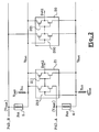
- FIG. 2 represents an exemplary embodiment of comparison circuits used in a protection according to the invention.
- each circuit consists of practice in at least two inverters, a first, for compare internal line voltage levels supply and input / output pad, a second to reshape the signal obtained and provide the detection signal at output.
- the circuits of comparison 20 and 21 for the two internal lines BV1 and BV2 power supply In the case of the line internal supply BV1, the comparison circuit 20 associated allows to detect that the voltage level V1int of this line is below the voltage level the PAD-B input-output pad around a threshold of transistor. In the case of the internal line power supply BV2, the comparison circuit 21 associated to detect that the voltage level V2int of this line is higher than the voltage level the PAD-A input-output pad around a threshold of transistor.
- the comparison circuit 20 associated with the line internal supply BV1 thus includes a first inverter 200 and a second inverter 201.
- the first inverter 200 is supplied between the stud input / output PAD-B and the internal line BV2 power supply.
- the input of this inverter is connected to the internal supply line BV1.
- the output of the inverter remains at low level. If the level V1int of the input voltage becomes lower than the PAD-B stud voltage level, the output of the inverter switches to high level, this which provides detection according to the invention. In practice, it is enough that the level V1int becomes lower by one transistor threshold at the voltage level of the pad PAD-B. Preferably, the transistors of the inverter 200 of the comparison circuit are chosen to have a lowest possible threshold voltage.
- the second inverter 201 is supplied in the normal way, by the two internal supply lines BV1 and BV2 and allows to reshape the output signal of the first inverter.
- the comparison circuit 21 associated with the internal supply line BV2 thus includes a first inverter 210 and a second inverter 211.
- the first inverter 210 is supplied between the line internal BV1 power supply and input / output pad PAD-A. The input of this inverter is connected to the internal supply line BV2.
- the output of the inverter remains at high level. If the level V2int of the input voltage becomes higher than the level of the PAD-A stud voltage, the output of the inverter switches to low level, this which provides detection according to the invention. In practice, it is enough that the level V2int becomes higher by one transistor threshold at the voltage level of pad PAD-A. Preferably, the transistors of the inverter 210 of the comparison circuit is chosen to have a lowest possible threshold voltage.
- the second inverter 211 is supplied in the normal way, by the two internal supply lines BV1 and BV2 and allows to reshape the output signal of the first inverter.
- the input / output pads PAD-A and PAD-B allowing internal power supply in case faulty connection on the power pads may be pads for receiving signals from control by which the integrated circuit is placed in one operating mode or another. These studs are then by default at voltage levels corresponding to a default operating mode. Changing the operating mode of the circuit integrated is ordered by imposing on one and / or the other plot a different logic voltage level over time of a front or a clock pulse. In such a case, detection according to the invention is permanent or almost permed. Such an operation corresponds in particular to the operating mode of integrated circuits intended for smart card type applications. But the invention does not apply exclusively to this type integrated circuit.
- any circuit integrated comprising at least one input / output pad connected to an internal power line by a pulling device, corresponding to the level of default voltage on this pad.
- there are other input / output pads associated with draw devices at one of the internal levels of supply voltage for example the stud clock transmission, usually associated with a ground pulling device or studs data input / output, usually associated with a pulling device at supply voltage positive logic Vdd.
- the comparison associated with such a pad is only active when the level of the stud is equal to the draw level.
Landscapes
- Physics & Mathematics (AREA)
- General Physics & Mathematics (AREA)
- Semiconductor Integrated Circuits (AREA)
- Tests Of Electronic Circuits (AREA)
Abstract
Description
- la figure 1 représente un schéma-bloc général d'un dispositif de détection selon l'invention dans un circuit intégré; et
- la figure 2 est un schéma détaillé d'un exemple de réalisation d'un dispositif de détection selon l'invention.
Claims (8)
- Dispositif de détection de mauvaise connexion d'alimentation dans un circuit intégré comprenant au moins un plot d'alimentation (PAD-V1) pour appliquer une alimentation externe (V1ext) sur une ligne interne d'alimentation (BV1) du circuit intégré et au moins un plot d'entrée/sortie (PAD-B) avec un dispositif de tirage (5) connecté entre ledit plot et la dite ligne d'alimentation interne, caractérisé en ce que le dispositif de détection comprend un circuit de comparaison (20) des niveaux de tension entre ledit plot et la dite ligne d'alimentation interne.
- Dispositif de détection selon la revendication 1, caractérisé en ce qu'il comprend -au moins un circuit de comparaison (20, 21) par plot d'alimentation (PAD-V1, PAD-V2) du circuit intégré.
- Dispositif selon la revendication 1 ou 2, caractérisé en ce qu'il comprend un circuit de comparaison entre le niveau de tension d'une ligne d'alimentation interne et chaque plot d'entrée/sortie auquel est associé un dispositif de tirage connecté entre ce plot et ladite ligne.
- Dispositif de détection selon l'une quelconque des revendications précédentes, caractérisé en ce qu'un circuit de comparaison (20) entre les niveaux de tension d'une ligne d'alimentation interne (BV1) et d'un plot d'entrée/sortie (PAD-B) comprend un inverseur (200) alimenté par ledit plot et connecté en entrée à la dite ligne d'alimentation interne.
- Dispositif de détection selon la revendication 4, caractérisé en ce que ledit inverseur (200) est formé de transistors ayant un seuil le plus petit possible.
- Dispositif de détection selon la revendication 4 ou 5, caractérisé en ce que ledit circuit de comparaison (20) comprend un autre inverseur (201) en série avec le premier, qui fournit en sortie un signal de détection (Det1).
- Dispositif de détection selon l'une quelconque des revendications précédentes, caractérisé en ce qu'il fournit en sortie un signal de détection (DET) appliqué comme signal de blocage du circuit intégré.
- Circuit intégré comprenant un dispositif de détection selon l'une quelconque des revendications précédentes.
Applications Claiming Priority (2)
| Application Number | Priority Date | Filing Date | Title |
|---|---|---|---|
| FR0101253 | 2001-01-30 | ||
| FR0101253A FR2820212A1 (fr) | 2001-01-30 | 2001-01-30 | Circuit de detection de mauvaise connexion d'alimentation |
Publications (2)
| Publication Number | Publication Date |
|---|---|
| EP1227329A1 true EP1227329A1 (fr) | 2002-07-31 |
| EP1227329B1 EP1227329B1 (fr) | 2004-04-14 |
Family
ID=8859414
Family Applications (1)
| Application Number | Title | Priority Date | Filing Date |
|---|---|---|---|
| EP02290165A Expired - Lifetime EP1227329B1 (fr) | 2001-01-30 | 2002-01-23 | Circuit de détection de mauvaise connexion d'alimentation |
Country Status (4)
| Country | Link |
|---|---|
| US (1) | US6774663B2 (fr) |
| EP (1) | EP1227329B1 (fr) |
| DE (1) | DE60200351D1 (fr) |
| FR (1) | FR2820212A1 (fr) |
Cited By (1)
| Publication number | Priority date | Publication date | Assignee | Title |
|---|---|---|---|---|
| US9466979B2 (en) | 2011-08-18 | 2016-10-11 | Infineon Technologies Ag | Communication line driver protection circuitry, systems and methods |
Families Citing this family (10)
| Publication number | Priority date | Publication date | Assignee | Title |
|---|---|---|---|---|
| US7365596B2 (en) * | 2004-04-06 | 2008-04-29 | Freescale Semiconductor, Inc. | State retention within a data processing system |
| CN100547419C (zh) * | 2005-01-06 | 2009-10-07 | 联发科技股份有限公司 | 电池侦测系统及其方法 |
| US20060212377A1 (en) * | 2005-03-16 | 2006-09-21 | Ubs Ag | Method and system for analyzing and reporting equity compensation |
| GB2452732A (en) * | 2007-09-12 | 2009-03-18 | Seiko Epson Corp | Smart-card chip with organic conductive surface layer for detecting invasive attack |
| JP5301262B2 (ja) | 2008-12-19 | 2013-09-25 | ルネサスエレクトロニクス株式会社 | 半導体装置、及び動作モ−ド切換方法 |
| US8340933B1 (en) * | 2009-09-30 | 2012-12-25 | Emc Corporation | Method and apparatus for performing power supply self-diagnostics in redundant power architectures |
| US8427171B2 (en) * | 2010-06-07 | 2013-04-23 | Steve Carkner | Battery connection failure detection system |
| TWI562156B (en) | 2011-05-13 | 2016-12-11 | Semiconductor Energy Lab Co Ltd | Semiconductor device |
| US10692581B2 (en) * | 2017-01-18 | 2020-06-23 | Microchip Technology Incorporated | Circuits for bleeding supply voltage from a device in a power down state |
| KR102637795B1 (ko) * | 2017-02-10 | 2024-02-19 | 에스케이하이닉스 주식회사 | 반도체 장치 |
Citations (3)
| Publication number | Priority date | Publication date | Assignee | Title |
|---|---|---|---|---|
| JPH01237894A (ja) * | 1988-03-18 | 1989-09-22 | Hitachi Maxell Ltd | 半導体記録装置の端子接続検出方式 |
| JPH06325222A (ja) * | 1993-05-18 | 1994-11-25 | Fuji Electric Co Ltd | Icカードリーダライタ |
| JP2001005916A (ja) * | 1999-06-22 | 2001-01-12 | Matsushita Electric Ind Co Ltd | Icカードリーダ・ライタ |
Family Cites Families (1)
| Publication number | Priority date | Publication date | Assignee | Title |
|---|---|---|---|---|
| US6027029A (en) * | 1997-04-21 | 2000-02-22 | Samsung Electronics Co., Ltd | Smart card capable of adjusting voltages supplied from external device |
-
2001
- 2001-01-30 FR FR0101253A patent/FR2820212A1/fr active Pending
-
2002
- 2002-01-23 EP EP02290165A patent/EP1227329B1/fr not_active Expired - Lifetime
- 2002-01-23 DE DE60200351T patent/DE60200351D1/de not_active Expired - Lifetime
- 2002-01-29 US US10/060,105 patent/US6774663B2/en not_active Expired - Lifetime
Patent Citations (3)
| Publication number | Priority date | Publication date | Assignee | Title |
|---|---|---|---|---|
| JPH01237894A (ja) * | 1988-03-18 | 1989-09-22 | Hitachi Maxell Ltd | 半導体記録装置の端子接続検出方式 |
| JPH06325222A (ja) * | 1993-05-18 | 1994-11-25 | Fuji Electric Co Ltd | Icカードリーダライタ |
| JP2001005916A (ja) * | 1999-06-22 | 2001-01-12 | Matsushita Electric Ind Co Ltd | Icカードリーダ・ライタ |
Non-Patent Citations (3)
| Title |
|---|
| PATENT ABSTRACTS OF JAPAN vol. 013, no. 570 (P - 977) 18 December 1989 (1989-12-18) * |
| PATENT ABSTRACTS OF JAPAN vol. 1995, no. 02 31 March 1995 (1995-03-31) * |
| PATENT ABSTRACTS OF JAPAN vol. 2000, no. 16 8 May 2001 (2001-05-08) * |
Cited By (1)
| Publication number | Priority date | Publication date | Assignee | Title |
|---|---|---|---|---|
| US9466979B2 (en) | 2011-08-18 | 2016-10-11 | Infineon Technologies Ag | Communication line driver protection circuitry, systems and methods |
Also Published As
| Publication number | Publication date |
|---|---|
| DE60200351D1 (de) | 2004-05-19 |
| FR2820212A1 (fr) | 2002-08-02 |
| EP1227329B1 (fr) | 2004-04-14 |
| US6774663B2 (en) | 2004-08-10 |
| US20020135379A1 (en) | 2002-09-26 |
Similar Documents
| Publication | Publication Date | Title |
|---|---|---|
| EP1227329B1 (fr) | Circuit de détection de mauvaise connexion d'alimentation | |
| EP1200927B1 (fr) | Lecteur de carte a puce comprenant un systeme d'economie d'energie | |
| EP0267114B1 (fr) | Circuit intégré pour la mémorisation et le traitement d'informations de manière confidentielle comportant un dispositif anti-fraude | |
| FR2916560A1 (fr) | Cryptoprocesseur a protection de donnees amelioree | |
| KR100260989B1 (ko) | 입력 버퍼 회로 | |
| EP2466528B1 (fr) | Sécurisation de l'alimentation de moyens de commande d'une carte à microcircuit en cas d'attaque | |
| EP0581639B1 (fr) | Dispositif de protection d'un circuit intégré contre les coupures d'alimentation | |
| WO1999034223A1 (fr) | Circuit electronique de surveillance de tension electrique | |
| FR2563026A1 (fr) | Dispositif de controle pour des amplificateurs d'attaque integres | |
| EP1053531B2 (fr) | Dispositif a circuit integre securise par attenuation de signatures electriques | |
| EP1758029A1 (fr) | Périphérique USB sécurisé | |
| EP0450245A2 (fr) | Détecteur de variation rapide d'alimentation de circuit intégré | |
| FR2857111A1 (fr) | Microcontroleur a protection logique contre les decharges electrostatiques | |
| EP1672795A1 (fr) | Dispositif de réinitialisation d'un circuit intégré à partir d'une détection d'une chute d'une tension d'alimentation, et circuit électronique correspondant | |
| JP2000065880A (ja) | 結線状況検出回路及びその結線状況検出回路を備えたicチップ内蔵媒体 | |
| FR2661269A1 (fr) | Cartes a circuits integres. | |
| EP1887494A1 (fr) | Dispositif électronique disposant de plusieurs interfaces de communication court-circuitables | |
| EP0996102B1 (fr) | Procédé de contrôle d'un terminal muni d'un connecteur de carte à micromodules à contacts | |
| EP1109026B1 (fr) | Dispositif de détection d'une haute tension | |
| EP2203862B1 (fr) | Echange de donnees entre un terminal de paiement electronique et un outil de maintenance par une liaison usb | |
| US7009879B2 (en) | Test terminal negation circuit for protecting data integrity | |
| US7321235B2 (en) | Input circuit for an integrated circuit | |
| EP0405353B1 (fr) | Dispositif de protection pour système de transmission de signaux numériques | |
| FR2853475A1 (fr) | Circuit integre delivrant des niveaux logiques a une tension independante de la tension d'alimentation, sans regulateur associe pour la partie puissance, et module de communication correspondant | |
| JP2000338928A (ja) | 車載用lcdモニタの保護装置及びその保護方法 |
Legal Events
| Date | Code | Title | Description |
|---|---|---|---|
| PUAI | Public reference made under article 153(3) epc to a published international application that has entered the european phase |
Free format text: ORIGINAL CODE: 0009012 |
|
| AK | Designated contracting states |
Kind code of ref document: A1 Designated state(s): AT BE CH CY DE DK ES FI FR GB GR IE IT LI LU MC NL PT SE TR |
|
| AX | Request for extension of the european patent |
Free format text: AL;LT;LV;MK;RO;SI |
|
| 17P | Request for examination filed |
Effective date: 20021017 |
|
| AKX | Designation fees paid |
Designated state(s): DE FR GB IT |
|
| 17Q | First examination report despatched |
Effective date: 20030324 |
|
| GRAP | Despatch of communication of intention to grant a patent |
Free format text: ORIGINAL CODE: EPIDOSNIGR1 |
|
| RTI1 | Title (correction) |
Free format text: DETECTOR CIRCUIT FOR A POOR POWER SUPPLY CONNECTION |
|
| GRAS | Grant fee paid |
Free format text: ORIGINAL CODE: EPIDOSNIGR3 |
|
| GRAA | (expected) grant |
Free format text: ORIGINAL CODE: 0009210 |
|
| RIN1 | Information on inventor provided before grant (corrected) |
Inventor name: MOREAUX, CHRISTOPHE Inventor name: KARI, AHMED |
|
| AK | Designated contracting states |
Kind code of ref document: B1 Designated state(s): DE FR GB IT |
|
| PG25 | Lapsed in a contracting state [announced via postgrant information from national office to epo] |
Ref country code: IT Free format text: LAPSE BECAUSE OF FAILURE TO SUBMIT A TRANSLATION OF THE DESCRIPTION OR TO PAY THE FEE WITHIN THE PRESCRIBED TIME-LIMIT;WARNING: LAPSES OF ITALIAN PATENTS WITH EFFECTIVE DATE BEFORE 2007 MAY HAVE OCCURRED AT ANY TIME BEFORE 2007. THE CORRECT EFFECTIVE DATE MAY BE DIFFERENT FROM THE ONE RECORDED. Effective date: 20040414 |
|
| REG | Reference to a national code |
Ref country code: GB Ref legal event code: FG4D Free format text: NOT ENGLISH |
|
| REF | Corresponds to: |
Ref document number: 60200351 Country of ref document: DE Date of ref document: 20040519 Kind code of ref document: P |
|
| REG | Reference to a national code |
Ref country code: IE Ref legal event code: FG4D Free format text: FRENCH |
|
| PG25 | Lapsed in a contracting state [announced via postgrant information from national office to epo] |
Ref country code: DE Free format text: LAPSE BECAUSE OF FAILURE TO SUBMIT A TRANSLATION OF THE DESCRIPTION OR TO PAY THE FEE WITHIN THE PRESCRIBED TIME-LIMIT Effective date: 20040715 |
|
| GBT | Gb: translation of ep patent filed (gb section 77(6)(a)/1977) |
Effective date: 20040716 |
|
| REG | Reference to a national code |
Ref country code: IE Ref legal event code: FD4D |
|
| PLBE | No opposition filed within time limit |
Free format text: ORIGINAL CODE: 0009261 |
|
| STAA | Information on the status of an ep patent application or granted ep patent |
Free format text: STATUS: NO OPPOSITION FILED WITHIN TIME LIMIT |
|
| 26N | No opposition filed |
Effective date: 20050117 |
|
| PGFP | Annual fee paid to national office [announced via postgrant information from national office to epo] |
Ref country code: GB Payment date: 20081229 Year of fee payment: 8 |
|
| PGFP | Annual fee paid to national office [announced via postgrant information from national office to epo] |
Ref country code: FR Payment date: 20090128 Year of fee payment: 8 |
|
| GBPC | Gb: european patent ceased through non-payment of renewal fee |
Effective date: 20100123 |
|
| REG | Reference to a national code |
Ref country code: FR Ref legal event code: ST Effective date: 20100930 |
|
| PG25 | Lapsed in a contracting state [announced via postgrant information from national office to epo] |
Ref country code: FR Free format text: LAPSE BECAUSE OF NON-PAYMENT OF DUE FEES Effective date: 20100201 |
|
| PG25 | Lapsed in a contracting state [announced via postgrant information from national office to epo] |
Ref country code: GB Free format text: LAPSE BECAUSE OF NON-PAYMENT OF DUE FEES Effective date: 20100123 |