EP1225596A2 - Programming and erasing methods for a reference cell of an NROM array - Google Patents
Programming and erasing methods for a reference cell of an NROM array Download PDFInfo
- Publication number
- EP1225596A2 EP1225596A2 EP01309289A EP01309289A EP1225596A2 EP 1225596 A2 EP1225596 A2 EP 1225596A2 EP 01309289 A EP01309289 A EP 01309289A EP 01309289 A EP01309289 A EP 01309289A EP 1225596 A2 EP1225596 A2 EP 1225596A2
- Authority
- EP
- European Patent Office
- Prior art keywords
- programming
- level
- voltage
- threshold voltage
- cell
- Prior art date
- Legal status (The legal status is an assumption and is not a legal conclusion. Google has not performed a legal analysis and makes no representation as to the accuracy of the status listed.)
- Granted
Links
Images


Classifications
-
- G—PHYSICS
- G11—INFORMATION STORAGE
- G11C—STATIC STORES
- G11C11/00—Digital stores characterised by the use of particular electric or magnetic storage elements; Storage elements therefor
- G11C11/56—Digital stores characterised by the use of particular electric or magnetic storage elements; Storage elements therefor using storage elements with more than two stable states represented by steps, e.g. of voltage, current, phase, frequency
- G11C11/5671—Digital stores characterised by the use of particular electric or magnetic storage elements; Storage elements therefor using storage elements with more than two stable states represented by steps, e.g. of voltage, current, phase, frequency using charge trapping in an insulator
-
- G—PHYSICS
- G11—INFORMATION STORAGE
- G11C—STATIC STORES
- G11C16/00—Erasable programmable read-only memories
- G11C16/02—Erasable programmable read-only memories electrically programmable
- G11C16/04—Erasable programmable read-only memories electrically programmable using variable threshold transistors, e.g. FAMOS
- G11C16/0466—Erasable programmable read-only memories electrically programmable using variable threshold transistors, e.g. FAMOS comprising cells with charge storage in an insulating layer, e.g. metal-nitride-oxide-silicon [MNOS], silicon-oxide-nitride-oxide-silicon [SONOS]
- G11C16/0475—Erasable programmable read-only memories electrically programmable using variable threshold transistors, e.g. FAMOS comprising cells with charge storage in an insulating layer, e.g. metal-nitride-oxide-silicon [MNOS], silicon-oxide-nitride-oxide-silicon [SONOS] comprising two or more independent storage sites which store independent data
-
- G—PHYSICS
- G11—INFORMATION STORAGE
- G11C—STATIC STORES
- G11C16/00—Erasable programmable read-only memories
- G11C16/02—Erasable programmable read-only memories electrically programmable
- G11C16/06—Auxiliary circuits, e.g. for writing into memory
- G11C16/10—Programming or data input circuits
- G11C16/14—Circuits for erasing electrically, e.g. erase voltage switching circuits
-
- G—PHYSICS
- G11—INFORMATION STORAGE
- G11C—STATIC STORES
- G11C16/00—Erasable programmable read-only memories
- G11C16/02—Erasable programmable read-only memories electrically programmable
- G11C16/06—Auxiliary circuits, e.g. for writing into memory
- G11C16/34—Determination of programming status, e.g. threshold voltage, overprogramming or underprogramming, retention
- G11C16/3436—Arrangements for verifying correct programming or erasure
- G11C16/3468—Prevention of overerasure or overprogramming, e.g. by verifying whilst erasing or writing
- G11C16/3481—Circuits or methods to verify correct programming of nonvolatile memory cells whilst programming is in progress, e.g. by detecting onset or cessation of current flow in cells and using the detector output to terminate programming
-
- G—PHYSICS
- G11—INFORMATION STORAGE
- G11C—STATIC STORES
- G11C16/00—Erasable programmable read-only memories
- G11C16/02—Erasable programmable read-only memories electrically programmable
- G11C16/06—Auxiliary circuits, e.g. for writing into memory
- G11C16/26—Sensing or reading circuits; Data output circuits
- G11C16/28—Sensing or reading circuits; Data output circuits using differential sensing or reference cells, e.g. dummy cells
-
- G—PHYSICS
- G11—INFORMATION STORAGE
- G11C—STATIC STORES
- G11C2211/00—Indexing scheme relating to digital stores characterized by the use of particular electric or magnetic storage elements; Storage elements therefor
- G11C2211/56—Indexing scheme relating to G11C11/56 and sub-groups for features not covered by these groups
- G11C2211/563—Multilevel memory reading aspects
- G11C2211/5634—Reference cells
Definitions
- the present invention relates generally to electrically erasable, programmable read only memory (EEPROM) cells and specifically, to methods for programming thereof.
- EEPROM electrically erasable, programmable read only memory
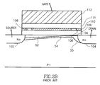
- Fig. 1 illustrates a typical prior art floating gate cell, comprising two diffusion areas, source 102 and drain 104, embedded in a substrate 105, between which is a channel 100.
- a floating gate 101 is located above but insulated from channel 100, and a gate 112 is located above but insulated from floating gate 101.
- programming voltages V G and V D are applied to gate 101 and drain 104, respectively, and a low source voltage V S is applied to source 102.
- a row of gates are formed into a word line, and a column of drain and source are formed into bit lines along which voltages V D and V S , respectively, are supplied.
- the source and drain voltages V S and V D create a lateral field that pulls channel electrons from source 102 to drain 104. This is indicated by arrow 10.
- a vertical field created by the gate voltage V G allows hot channel electrons to be injected (arrow 12) into floating gate 101. Once injected into floating gate 101, the electrons are distributed equally across the entire gate, increasing the threshold voltage V TH of gate 101.
- Non-volatile cell is the nitride, read only memory (NROM) cells are described in US 6,011,725, assigned to the common assignee of the present application. The disclosure of US 6,011,725 is incorporated herein by reference.
- NROM read only memory
- the NROM cell illustrated in Figs. 2A and 2B Similar to the floating gate cell of Fig. 1, the NROM cell illustrated in Figs. 2A and 2B, to which reference is now made, has channel 100 between two diffusion areas 102 and 104. However, unlike the floating gate cell, the NROM cell has two separated and separately chargeable areas 106 and 108. Each chargeable area defines one bit. For the dual bit cell of Figs. 2, the separately chargeable areas 106 and 108 are found within a nitride layer 110 formed in an oxide-nitride-oxide (ONO) sandwich (layers 109, 110 and 111) underneath gate 112.
- ONO oxide-nitride-oxide
- the left diffusion area 102 receives the high programming voltage V D (i.e. area 102 is the drain) and right diffusion area 104 is grounded (i.e. area 104 is the source). Hence the electrons flow from area 104 to area 102. This is indicated by arrow 114. The channel hot electrons are then injected into the nitride layer, in area 106. The negative charge in area 106 raises the threshold voltage of the cell, if read in the reverse direction.
- programming area 108 the left diffusion area 102 is the source (i.e. grounded) and right diffusion area 104 is the drain (i.e. receives high programming voltage V D ).
- the cell is therefore programmed in the opposite direction, as indicated by arrow 113, and the electrons then jump up into chargeable area 108.
- each bit is read in the direction opposite (a "reverse read") to that of its programming direction.
- a reverse read An explanation of the reverse read process is described in U.S. 6,011,725, mentioned above.
- right diffusion area 104 is the drain and left diffusion area 102 is the source. This is known as the "read through” direction, indicated by arrow 113.
- the cell is read in the opposite direction, indicated by arrow 114.
- left diffusion area 102 is the drain and right diffusion area 104 is the source.
- the presence of the gate and drain voltages V G and V D induce a depletion layer 54 (Fig. 2B) and an inversion layer 52 in the center of channel 100.
- the drain voltage V D is large enough to induce a depletion region 55 near drain 104 which extends to the depletion layer 54 of channel 100. This is known as “barrier lowering" and it causes “punch-through” of electrons from the inversion layer 52 to the drain 104.
- area 106 is near left diffusion area 102 which, for this case, acts as the source (i.e. low voltage level)
- the charge state of area 106 will determine whether or not the inversion layer 52 is extended to the source 102. If enough electrons are trapped in left area 106, then the voltage thereacross will not be sufficient to extend inversion layer 52 to the source 102, the cells current will be low, and a "0" will be read. The opposite is true if area 106 has no charge.
- Figs. 3A, 3B and 3C are timing diagrams of an exemplary prior art programming schedule for NROM cells.
- programming pulses 120A, 120B and 120C consisting of programming voltages V D , V S , and V G , respectively, are applied to the cell.
- Programming pulses 120 are then followed by program verify pulses 122A, 122B and 122C, consisting of read voltages V D , V S , and V G , respectively, during which time the cell is read.
- bit If there are enough electrons trapped in the bit, a "0" is read, and the cell is verified as programmed. If, however, during the read operation, the inversion layer is not strong enough to prevent the current flow through the channel, then the bit will be read as a "1", and the cell will fail program verification.
- the sequence of pulses 120 and 122 are repeatedly applied until the effect of the charged trapped in area 106 (or 108) has reached the desired level and the cell is considered "programmed". The programming process is then terminated.
- the first requirement can easily be met just by increasing the drain and gate potentials to their maximum values.
- this strategy will not meet the second requirement due to the many process and environmental parameters that affect the programming rate and its variations.
- Nonvolatile Multilevel Memories for Digital Applications discusses a number of proposed methods for programming multi-level floating gate circuits, including that of controlling the programming time length.
- One such method is discussed in the section Programming and Accuracy, 2) Drain Voltage Programming, as follows: 1) a constant gate voltage is set, 2) per bit level of the multi-level cell, a constant drain voltage is determined, and 3) the cell is programmed for a predetermined time period. At the completion of the time period, the programming is terminated.
- the article describes an approach whereby after each programming pulse, the threshold voltage V TH is verified. Upon reaching the target threshold voltage, programming is terminated.
- U.S. Patent 5,523,972 describes a floating gate method that entails incrementally increasing the programming gate voltage V G , while keeping other factors constant (e.g. source and drain voltages, V S and V D , respectively).
- each cell is checked to determine whether or not it has reached the desired state. If not, a programming gate voltage pulse of a slightly higher voltage is applied to the cell. The charge level is checked again, and if the desired state has not yet been reached, the voltage is raised again and applied. This process is repeated until all the cells reach the desired level.
- US Patent 5,172,338 describes a programming algorithm similar to that described in the U.S. Patent 5,523,972, however, on a per cell basis. Every cell that reaches the desired level does not receive the drain voltage of the next step. This sequence is continued until the last bit of the byte word/group is programmed.
- Fig. 4 illustrates the typical variation of programming time for a normal population of memory cells.
- Point 126 depicts the cell with the fastest programming speed
- point 128 represents the cell with the slowest programming speed.
- the variance in time between point 126 to point 128 can be as large as 500x.
- Some of the factors influencing the programming speed in floating gate cells are: variations in process parameters such as channel length, gate coupling ratio, drain coupling ratio, source resistance variations (array effect) and channel doping variations.
- Another factor influencing the program rate is the temperature of the product during programming; generally, the lower the temperature, the faster the programming rate.
- the parameters that affect the programming speed are: the ONO thickness, the channel length, the channel doping and the temperature.
- the programming state of one bit affects the programming speed of the other bit.
- Fig. 5 a graph illustrating the different threshold voltage levels comprised within a multi-level floating gate cell.
- each bit in the multi-level floating gate cell is defined by a predefined region of voltage threshold V TH .
- the first bit lies in region 132, (to the left of line W), while the second bit lies in region 134 (from line W to line X), the third bit in region 136 (from line X to line Y), and so on.
- the resultant threshold voltage may overshoot the desired region, thus leading to a read error or failure.
- NROM cells in addition to the stated problems connected with breakdown of the oxide layer and unnecessary dissipation of power, over-programming creates different problems. As explained below in connection with Figs. 6, over-programming results in quality deterioration and reliability degradation, as well as read failures in two-bit cells.
- Figs. 6A, 6B, 6C and 6D are exploded views of the NROM cell depicted in Figs. 2A and 2B. It is noted that the shape of the trapped charge in chargeable areas 106 and 108 range from a narrow pocket, depicted as 106N and 108N, to an average pocket (i.e. 106A and 108A), to an even wider pocket (i.e. 106W and 108W) with a "tail" 44.
- tail 44 which is farther from the bit line than the bulk of the trapped charge, is generally not removable during erasure and thus, reduces the ability of the NROM cell to withstand a large number of program and erase cycles. Typically, erasure depletes only the charge concentration closest to the diffusion area. Thus, if the distribution pocket is too wide, the tail 44 of the trapped charge will not erase, and with each progressive erase, more and more charge will remain in the retention section, even after erasures (Fig. 6D).
- the trapped charge in tail 44 acts as partially programmed charge. It is due to the trapped charge in tail 44 that fewer programming pulses are required to achieve the programmed threshold voltage level (since the bit is already, in effect, partially programmed).
- the accumulation of trapped negative charge far from the junction increases the threshold voltage level, which affects the reverse read, making it difficult to distinguish the first bit from the second bit and creating read failures.
- the erase operation accumulates extra positive charge close to the junction, which makes the erase time take longer.
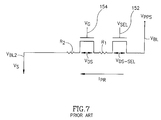
- FIG. 7 an electrical schematic of a portion of an NROM array.
- the depicted circuit includes a bit line power supply V PPS , a select transistor 152, resistors R1 and R2, and an NROM cell 154.
- Resistors R1 and R2 denote the native resistance of the wire in the depicted array.
- Transistor 152 is a select transistor used to select a bit line of the array.
- Programming current I PR flows throughout the entire circuit. The voltage drops across the channels of transistor 152 and cell 154 are designated as V DS-SEL and V DS , respectively.
- the desired gate voltage V G is set relatively high, i.e. 8 - 10V.
- Further increases in gate voltage V G such as over 10V, require special processes and put severe limitations on the scaling of the ONO thickness due to charging by tunneling. For example, a 180 ⁇ ONO of the 0.5 ⁇ m process will experience tunneling charging for voltages over 12V.
- the second problem noted above creates even more severe limitations on the stepped gate voltage V G approach.
- the programming drain voltage V D must be fixed and high in order to cover a large dynamic range.
- Using a high programming drain voltage V D creates a large lateral field and a wide pinch-off regime, yielding a wide trapped charge region. Accordingly, the resultant product is the undesirable tail 44, which drastically reduces the product's endurance.
- stepping the programming gate voltage V G does not provide tight programming control and is not effective in preventing over-programming and eventual degradation of the product's quality.
- a method for programming a reference cell of a memory array includes the steps of programming the reference cell with large programming steps until a threshold voltage level of the reference cell is above an interim target level and programming the reference cell with small programming steps until the threshold voltage level is above a final target level.
- a method for programming a reference cell of a memory array which uses programming pulses. If a threshold voltage of the reference cell is below an interim target level, the method includes the step of raising a drain voltage for a next programming pulse and otherwise, setting the drain voltage for the next programming pulse at a fixed level not higher than a current level. Programming pulses are provided using the fixed drain voltage level until the threshold voltage level is at or above a final target level above the interim target level.
- the programming pulses have a different duration than the programming pulse for the step of raising.
- the interim target level is in the range of 100 - 400mV below the final target level.
- the interim target level is below the final target level by an amount generally not smaller than an expected threshold voltage change due to the programming pulses of the raising step.
- the method also includes the step of measuring the programmed threshold voltage level after each programming pulse.
- the method also includes the step of determining after each programming pulse if the programmed threshold voltage is above or below the target level.
- a method for programming a reference cell of a memory array which includes the steps of fast programming of the reference cell until a threshold voltage level of the reference cell is above an interim target level and slow programming of the reference cell until the threshold voltage level is above a final target level which is above the interim target level.
- the fast programming comprises providing programming pulses and changing a drain voltage level between programming pulses.
- the slow programming comprises maintaining a generally constant drain voltage level between programming pulses.
- the steps of programming include providing programming pulses and also include the step of measuring the threshold voltage level of the reference cell after each programming pulse.
- a method for programming a reference cell of a memory array which includes the steps of programming the reference cell with large programming steps until a threshold voltage level of the reference cell is above an interim target level and programming the reference cell with small programming steps until the threshold voltage level is above a final target level.
- the programming with large programming steps includes providing programming pulses and changing a drain voltage level between programming pulses.
- the programming with small programming steps comprises maintaining a generally constant drain voltage level between programming pulses.
- the present invention teaches an NROM cell algorithm which regulates the bit line voltage V BL provided to the bit line acting as the drain, thereby providing tight programming control. Furthermore, the described invention provides the combination of a fast programming algorithm with reduced over-programming risk, and hence improved product endurance and cycling ability.
- references to the bit line voltage V BL refer to the voltage provided to the bit line currently acting as a drain.
- V BL the voltage provided to the bit line currently acting as a drain.
- the present invention further teaches the use of a low programming bit line voltage V BL to produce a tight spatial distribution of trapped charge, thereby resulting in better two-bit separation in the NROM cell, faster erase, and increased product life.
- Figs. 8A - 8C a series of graphs that illustrate the effect of the programming bit line voltage V BL on threshold voltage V TH as a function of cell temperature, channel length, and array effects/second bit, respectively.
- the reverse read threshold voltage V TR which is the threshold voltage V TH when the cell is reverse read, is a function of bit line voltage V BL . Every point represents a programming pulse of 2 ⁇ sec in exemplary steps of 0.3V. It is noted that the gate voltage V G is constant at 9V.
- the graph in Fig. 8A illustrates 3 programming curves for three varying cell temperatures: curve 202 denotes a cell at -40°C, curve 204 - a cell at 20°C, and curve 206 - a cell at 80°C.
- each cell receives a different drain voltage V D , depending on the temperature of that specific cell.
- V TH the low temperature case
- V BL bit line voltage
- V BL bit line voltage
- the bit line voltage V BL is incrementally increased from a minimum voltage to a higher voltage, thus covering a wide range of operating temperatures.
- the programming algorithm for that cell is terminated. Meanwhile, for cells which have not yet reached the desired threshold voltage, the bit line voltage V BL is incrementally increased, until those cells have reached their desired level.
- V TH the desired threshold voltage
- the bit line voltage V BL is incrementally increased, until those cells have reached their desired level.
- the bit line voltages V BL of 4.3V and 5V are the first bit line voltage levels that result in a threshold voltage V TH higher than the exemplary target of 4V.
- the chosen step size for the bit line voltage V BL affects the size of the maximum overshoot (over-programming) of the threshold voltage V TH .
- the step size is relatively small.
- the resultant algorithm requires many programming steps and may result in extended programming times.
- a large voltage step results in quicker programming times however, opens up to the risk of a large overshoot.
- the practical step size is a compromise between the requirements for quick programming speed and limited overshoot.
- Fig. 8B is comparable to the graph of Fig. 8A and depicts the effect of the bit line voltage V BL on the reverse read threshold voltage V TH as a function of a channel length of 0.6 ⁇ m, 0.65 ⁇ m and 0.7 ⁇ m respectively, for curves 212, 214, and 216, respectfully.
- Fig. 8C depicts the effect of the bit line voltage V BL on the reverse read threshold voltage V TH as a function of the location of a cell along a 32 bit long local diffusion bit-line segment and a comparison between the 1 st and 2 nd bit of the same cell.
- the fastest bit is bit 1 of word-line 16 and the slowest is bit 2 on word-lines 32 and 2.
- the fastest bit receives a bit line voltage V BL equal to approximately 5.8V, and the slowest, receives approximately 7V.
- the resultant programming algorithm when stepping the gate voltage V G , in order to catch the fast programming cells without risking over-programming, the resultant programming algorithm must commence with a low potential for the gate voltage V G . This, however, is undesirable since it causes programming to be slow. Hence, in order to increase the programming speed, the low gate voltage V G must be paired with high drain voltages V D .
- high drain voltages V D promotes cell degradation and decreased cycling ability.
- high drain voltages V D in combination with a low gate voltages V G are even more detrimental to the cell, producing very large lateral fields and wide pinch-off regions, yielding an extensive trapped charge region.
- the inventive programming algorithm commences with a low drain voltage V D , and a high gate voltage V G .
- V D low drain voltage
- V G high gate voltage
- V PS V DS + V DS-SEL + (R 1 +R 2 )*I PR
- Fig. 10 a graph illustrating the rise in threshold voltage V TH , as a function of time, with the bit line voltage V BL as a parameter. Depicted in Fig. 10 the resulting threshold voltage V TH for 4 exemplary drain voltages of 5V, 5.25V, 5.5V and 5.75 V, respectively.
- the threshold voltage V TH rises quickly at the start of the curve, and then reaches a point where the increase in threshold voltage V TH i is saturated.
- a progressively increasing drain voltage V D causes the threshold voltage V TH to climb along the steep slope of the programming function, and produces a more efficient and quicker programming algorithm.
- FIGs. 11A, 11B, and 11C a series of timing diagrams of a programming algorithm for NROM cells, constructed and operated in accordance with a preferred embodiment of the present invention.
- Figs. 11A - 11C illustrate only a limited number of pulses, it is apparent that a typical programming algorithm comprises numerous pulses and still complies with the principles of the present invention.
- Figs. 11A - 11C depict a programming algorithm utilizing gate voltage V G , drain voltage V D , and source voltage V S , respectively.
- the algorithm additionally comprises a series of alternating programming and program verify pulses.
- the first pulse is a programming pulse and is designated as A.
- the second pulse is a program verify pulse and is designated as B, and so on.
- the sequence of programming and program verify pulses A, B, C, etc. are repeatedly applied to an array of NROM cells. Once the threshold voltage V TH of an applicable cell has reached a desired level, the programming algorithm is terminated for that specific cell. The programming algorithm proceeds until each cell has reached the desired level, at which point the algorithm is terminated. Preferably the algorithm is applied on a bit by bit basis for either a byte, or word.
- the level of the drain voltage V D increases.
- the voltage steps are evenly incremented from progressive drain voltage V D pulse to pulse, i.e. at fixed increments of 0.25V, or any other desired increment.
- the present method teaches unevenly incremented voltage steps, i.e. with smaller incremented steps at the start of the algorithm and larger steps as the algorithm progresses. In this manner, the incremented steps directed to the "fast" programmers are smaller than the incremented steps for the "slow” programmers.
- the gate voltage V G is high and constant, (e.g. 10V) and the drain voltage V D is as low as possible, resulting in a narrow spatial distribution of trapped charge.
- the initial bit line voltage V D is approximately 4V.
- the resultant spatial distribution of the trapped charge 24 is closer to the diffusion area, which also facilitates effective erasure and increased life cycles. It is additionally noted that, due to the tighter spatial distribution of trapped charge, the present invention produces better two-bit separation and enables better distinction between the two bits during read. Furthermore, a smaller tail of trapped charge results in less erase time and voltage. This in turn, improves retention since less erase stress creates less trapped holes in the nitride. Less trapped holes, improves the retention since there is less trapped movement at the high temperature back.
- the final step of the drain voltage V D stops at a level that is just sufficient to reach the desired threshold voltage V TH , thus avoiding any unnecessary extra pulses of the drain voltage V D which might create secondary electron injections far from the junction, imposing the unwanted tail 44.
- the applied source voltage V S is not necessarily ground or 0V. However, in order to provide a tight distribution of charge, it is preferable that source voltage V S be as close to 0V as possible, and preferably less than 0.5V.
- the present invention includes adapting the programming and erasure methods of an array to its particular circumstances.
- the speed of programming and erasure of a bit is a function of how it is manufactured, the current operating temperature, the power supply, the peripheral circuitry and, if there are two bits in the memory cell, the programmed state of the other bit.
- Having a programming and/or erasure method that is adaptable enables the memory array to be programmed and/or erased quickly in most circumstances, no matter how the operating and environmental conditions vary.
- the present invention presents two types of adaptations, one of the initial programming or erasure level and the other of the program or erasure step.
- the dial-in level is determined from the response of the bits of the array, as described hereinbelow, and thus, is adapted to the particular array.
- Fig. 12 illustrates the method, using the dial-in procedure, to determine the highest possible, initial programming level for the memory array. This method is generally performed once per array, as part of a sort or a test part of the manufacturing process, although it can be performed at other times as well. Reference is also made to Figs. 13A, 13B and 13C, which are useful in understanding the method of Fig. 12.
- a representative portion of the array is first programmed (step 300), where "programmed” means that the threshold voltage of each cell is above a predetermined “program verify” level.
- the representative portion should include enough bits to cover the expected variation in programming responses. For example, the portion can include a few bytes. If there are more than one bit per cell, the portion should include a selection of each type of bit. The portion should also include cells in different locations within a block and/or column of cells, since the paths to such, from the power supplies, are different and each path has a different resistance level.
- the cells of the representative portion may be chosen according to known array effects and to sensitive manufacturing areas in the array. Which cells are chosen is typically determined empirically.
- Fig. 13A graphs the bit line voltage V BL (in number of steps) and the number of bits that became programmed at that level. In the example of Fig. 13A, two bits became programmed at level 6, five at level 7, eight at level 8 and 4 at level 9.
- Level 6 is the lowest programming level and is thus, the bit line voltage V BL1 of the fastest bits (i.e. the bits programmed in six, rather than seven, eight or nine, steps). Thus, as Applicants have realized, all bits of the representative portion could begin the programming procedure at level 6. In such a case, the fastest bits would be programmed in one step while the others would be programmed in two, three or four steps.
- the dial-in level DI is set to X levels lower than the fastest bit line voltage V BL1 , where X can be any reasonable margin, such as two or three levels.
- Fig. 13A shows (with arrow 306) setting the dial-in level DI to two levels lower than the stored bit line voltage V BL1 .
- Figs. 13B, 13C, 13D and 13E show four possible results. Since, in the four figures, the programming procedure begins at the dial-in level (the fourth original programming level), the first programming level in Figs. 13B - 13E is aligned with the fourth programming level of Fig. 13A. For all figures, the new bit line voltage V BL2 of the fastest bit is found in step 310.
- the fastest bits are as fast as the fastest ones in the representative portion and thus, program at the third programming level (which is equivalent to the old sixth programming level).
- the fastest bits program in two steps, and thus, are faster than those in the representative portion.
- the dial-in level DI is changed (step 312) to the fastest bit line voltage V BL2 .
- the fastest level is above the third programming level (as checked in step 314), meaning that the fastest bits in the remainder of the array are slower than those of the representative portion.
- the dial-in level DI is kept at the first fast programming level, V BL1 .
- the fastest programming level is the first one. This situation is inconclusive. It is possible that the fastest bit can program at an even lower programming level.
- the system now has a choice (steps 314 and 315); it can set the dial-in level DI to this first programming level, it can repeat the whole process from step 304, setting the preliminary dial-in level DI to lower than this level was previously, or it can decide to fail the part.
- the dial-in level DI is modified (step 312) to the either V BL1 or V BL2 , whichever is lowest.
- DI may be set to a lower level since the conditions during the test are not likely to match the expected conditions of operation. For example, the test may be performed at a fixed temperature while the product may be operated at lower or higher temperatures.
- Figs. 13B, 13C and 13D show that, by beginning the programming levels at a higher level than that of the original of Fig. 13A, the number of programming steps and thus, the programming time, is reduced. It should be noted that the first original steps cannot be omitted since, in some cases, the dial-in level DI may fall on the initial steps.
- the dial-in level DI is set to Y levels lower than the level set in step 312, where Y can be any reasonable margin to accommodate for temperature and cycling.
- Y can be one or two levels below the value found in step 312.
- the operation described hereinabove can be performed at other times during the life of the array, such as when so instructed by a user or by automatic built-in procedures.
- dial-in level DI determines quickly or roughly. In this case, only the representative portion is utilized and the dial-in level DI is set to the first fastest programming level V BL1 or, if desired, even higher. This choice may be adequate if fast programming is required.
- the method of changing the dial-in level generally improves yield since the initial programming pulses that hardly change the state of the bits are eliminated.
- Each programming pulse above the dial-in level is generally more effective and thus, most of the bits will not fail to program (a cause of reduced yield).
- Figs. 14A and 14B illustrate an exemplary method for dial-in for erasure.
- the basic method is similar to that of programming except that, in erasure, both the gate and the drain voltage levels may be set. This is shown in Figs. 14. Alternatively, only the drain voltage level can be set.
- the dial-in level DI of the gate or the drain is then set to a voltage level slightly below the voltage level of the slowest bit (to force the erase procedure to perform at least two erase pulses).
- step 320 the drain voltage Vppd is set to its lowest level for erasure.
- step 322 the gate voltage level is set to the least negative voltage possible for erasure.
- step 324 one or more representative bytes are programmed and, in step 326, a single erase pulse is provided. An erase verify operation is performed in step 328 and the results checked in step 330.
- step 331 If all of the bits which were programmed are now fully erased (i.e. the erase is fully verified), then either this occurred after the first loop (i.e. the gate is at its least negative level) or it occurred at some other point. This is checked in step 331. If the erasure occurred after the first loop (through steps 324 - 330), then the process was too successful and an error flag is set (step 333). Either the array can then be thrown away or the length of the erase pulse can be shortened and the process repeated.
- the gate voltage level for dial-in is set (step 332), as is the drain voltage Vppd for dial-in (step 335), and the process finishes in step 354.
- the gate voltage level for dial-in can be set to one level less negative than the current level.
- Other embodiments include setting the gate voltage for dial-in to the level found in this process or for setting it to Z levels less negative than the current level.
- step 330 If the erase verify (of step 330) was not successful, the gate voltage level is made more negative (step 334). As long as the gate voltage has not reached its most negative level (checked in step 336), the process of steps 324 through 330 is repeated with the new gate voltage level.
- the process continues with steps 338 - 348 by changing the drain voltage level.
- the gate level is set at this point to its most negative voltage level.
- step 338 the gate voltage is set to its most negative level.
- step 340 one or more representative bytes are programmed.
- the drain voltage is raised (step 342), after which, in step 344, a single erase pulse is provided.
- An erase verify operation is performed in step 346 and the results checked in step 348.
- the drain voltage Vppd for dial-in is set (step 352) and the process finished (step 354).
- the drain voltage Vppd for dial-in can be set to one level lower than the current level.
- Other embodiments include setting the drain voltage for dial-in to the level found in this process or for setting it to Z1 levels lower than the current level.
- step 350 If the bits are not yet fully erased, the process of steps 340 - 348 is repeated until a maximum drain voltage is reached, as checked by step 350. If the maximum drain voltage is reached and the bits have not been erased, then the array cannot be erased in one pulse. An error flag is set (step 356) and the process finished. At this point, the array may either be thrown away, the process of Figs. 14 may be repeated using two or more erase pulses in steps 326 and 344 or the duration of the erase pulse may be made longer.
- the dial-in level may also be determined by changing only the drain voltage Vppd (i.e. steps 320, 322 and 338 - 352).
- bit line programming levels increase in voltage by predetermined amounts.
- Figs. 15 and 16 illustrate a further embodiment of the present invention which changes the incremental voltage level of the drain Vppd between pulses in order to program most of the bits in as few programming steps as possible.
- the incremental voltage level is adapted to the current response of the bit to programming pulse.
- Bits respond to programming in different ways.
- the threshold voltage of some may increase significantly (see arrow 360 of Fig. 15) while the threshold voltage of others may only increase slightly (see arrow 362).
- the former bit requires only one more programming pulse (arrow 364) until it becomes programmed (i.e. until its threshold voltage is larger than a "program verify" voltage level).
- the latter type of bit must have multiple programming pulses (labeled 1 - 8) until it becomes programmed.
- Fig. 16 A bit that takes a significant number of programming pulses takes a long time to program and may limit the overall product performance.
- Applicants have realized that, if the threshold voltage level after a programming pulse is measured, it is possible to adjust the voltage level increment of the next programming pulse to move the threshold level toward the program verify level more quickly.
- Fig. 16 multiple verify levels, labeled verify 1, verify 2, verify 3 and verify 4, are shown.
- the present invention includes having multiple verify levels and that the four levels are shown for purposes of clarity only.
- the number of verify levels is a design choice and any number greater than one is included in the present invention. It will also be appreciated that existing reference levels in the array can be used to provide the multiple verify levels.
- the threshold voltage level of the bit is compared to five voltage levels, that of verify 1, verify 2, verify 3, verify 4 and program verify to determine how close to fully programmed the bit is.
- the first programming pulse brings the threshold voltage level of the first bit almost to the verify 3 level (this pulse is labeled 370A).
- the output of the comparisons will be that the threshold voltage level is above the verify 1 and verify 2 levels but not above the verify 3, verify 4 and program verify levels.
- the threshold level of the bit is thus above the verify 2 level.
- the first programming pulse brings the threshold voltage level to above the verify 1 level. Only the verify 1 comparison will indicate that the threshold level is above it; all the remaining comparisons will be that the threshold level of the bit is below the comparison level. Thus, the threshold level for the second exemplary bit is above the verify 1 level.
- comparison operations can be performed together or serially. If performed serially, from the program verify level down to the verify 1 level, then the comparison operation ends once the threshold level of the bit is above the current comparison level.
- a group of bits such as a byte
- the verify operation described hereinabove is performed for the group of bits and the bit having the highest verify level is then used to determine the size of the next programming pulse.
- Each verify level has a different voltage level increment associated therewith, depending on how far away the verify level is from the program verify level. The closer the verify level is to the program verify level, the smaller the increment to the drain voltage Vppd.
- the size of the increment depends on the average transfer function between the change ⁇ V PPD in bit line voltage and the resultant change ⁇ V T in threshold level and is typically determined by experimentation. In addition to depending on the change ⁇ V PPD , it can also depend on the level of the bit line voltage itself.
- the verify 4 level is 250mV less than the program verify level.
- the increment in bit line voltage level, ⁇ V PPD for a bit which is above the verify 4 level but below the program verify level is be about 300mV.
- Table 1 gives an example of voltage levels for the verify levels and their associated incremental voltage levels for the example of Fig. 16. Verify Name How much the reference level is less than the program verify Level (mV) ⁇ V PPD (mV) Program Verify 0 0 Verify 4 -250 300 Verify 3 -500 600 Verify 2 -750 900 Verify 1 -1000 1200
- the size of the increment is a tradeoff. If the minimum number of programming pulses is required, then the increment should be designed to bring a bit to fully programmed from whatever threshold voltage level it is at. Alternatively, if a minimum amount of overprogramming is desired, then the increment should be designed to bring a bit to just under the program verify level. The latter method requires that a further small increment programming pulse be performed in order to bring the bit above the program verify level. However, the latter method generally will not overprogram the bits.
- the process is repeated until one or more bits are fully programmed, at which point they no longer receive programming pulses.
- the bit with the next highest threshold level defines the increment for the next programming pulse.
- Fig. 16 shows this process.
- the first programming pulse 370 brought the first bit to above the verify 2 level, so the voltage level of the second programming pulse 374 is set to be large enough to bring the first bit to the program verify level. In this case, the second pulse was not quite large enough (arrow 374A does not quite reach the program verify level) and a third pulse 376 was necessary (arrow 376A is above the program verify level).
- second pulse 374 brings the threshold level above the verify 3 level (arrow 374B) and the third pulse brings the threshold level above the verify 4 level (arrow 376B).
- the second bit is the highest bit and its verify 4 level defines the increment for the fourth programming pulse, labeled 378, after which the second bit is fully programmed.
- step 380 the block to be erased is read and, in step 382, its erase state is checked. If all of the bits of the block are erased already, the process is finished (step 404).
- an erase pulse is provided (step 384), typically with predefined gate and drain voltages, such as those defined in the dial-in process of Fig. 14. Other predefined gate and drain voltages are also possible.
- the read level is decreased from the program verify level (i.e. the level of fully programmed bits) towards the erase verify level (i.e. fully erased) to determine how much erasure has occurred and how much more needs to occur.
- step 386 the read voltage level is set to the program verify (PV) level and the block is read (step 388). If all of the bits of the block pass the read operation, as checked in step 390, the read voltage level is reduced (step 394) as long as it has not yet reached the erase verify level (as checked in step 392).
- PV program verify
- step 404 If the read operation is successful at the erase verify level, then the block has been fully erased and the process finishes in step 404. However, if the read operation fails at some point, the drain voltage level Vppd is increased (step 396), for example, according to Table 2, another erase pulse is provided (step 400) using the new drain voltage level Vppd and the process is repeated from step 386. Step 398 checks that the number of erase pulses has not exceeded a maximum. If it has, then an error flag is set (step 402) and the process is stopped (step 404). Verify Name Reference Level above the Erase Verify Level (mV) ⁇ V PPD (mV) Program Verify 950 + 1000 Verify 2 700 +750 Verify 1 400 +500 Erase Verify 0 0
- Table 2 has only four verify levels while Table 1, for programming, has five verify levels.
- the number of verify levels are set by a designer according to any appropriate set of design considerations.
- the multiple verify levels of Fig. 16 are typically defined by the voltage level on or the current produced by a reference cell.
- Such reference cells may form sections of the memory array or they may be located outside of the memory array.
- the reference cell has a known and predefined set of characteristics which ensure that the voltage or current it produces when it receives a predefined set of gate, drain and source voltages is generally precise and reliable.
- a reference cell can either be unprogrammed or programmed. If the latter, the programming level should be well-defined to ensure that the reference cell has the desired characteristics. In contrast to programming an array cell, which should be programmed as fast as possible, programming a reference cell should be done as accurately as possible to ensure that the final threshold voltage Vt is at the desired level.
- Figs. 18A, 18B, 19A, 19B, 19C, 20A, 20B and 21, illustrate a method of programming reference cells in an NROM array.
- Fig. 18A indicates the target threshold voltage (Vt) levels for various reference cells
- Fig. 18B is similar to Fig. 16 and generally illustrates the operation of programming an exemplary reference cell
- Figs. 19A, 19B and 19C are a series of timing diagrams (similar to Figs. 11A - 11C) of the programming algorithm for reference cells
- Figs. 20A and 20B illustrate the evolution of the threshold voltage of two reference cells
- Fig. 21 provides an exemplary method in flow chart format.
- Fig. 18A shows some exemplary target threshold voltage Vt levels of reference cells to be programmed on a Vt axis.
- five target Vt levels for five different reference cells are shown (erase verify (EV), verify 1, verify 2, verify 3 and program verify (PV)) as is the initial distribution of threshold voltages of the native cells (i.e. prior to any programming).
- the threshold voltage of each reference cell must be brought to one of these target levels in order for them to act as reference levels for the array.
- Fig. 18B illustrates the operation for one reference level, verify 3.
- Fast stage 406 first moves the threshold voltage Vt of the reference cell from an initial threshold voltage 407 to the vicinity of an interim target level 409 that is below and close to the desired final target level (i.e. verify 3), where close may be, for example, within 300mV).
- the slow stage 408 'creeps' toward the final target level to ensure that, if the final target level is passed, it is passed by only a very small margin. This ensures the accuracy in the final level of the reference threshold voltage Vt.
- Fig. 18B shows also one example of the threshold voltage evolution when the cell is programmed according to one embodiment of the present invention.
- the threshold voltage Vt begins at initial level 407.
- the final target Vt of the cell is the verify 3 level, but the interim target Vt level for the fast stage is below it, (e.g. verify 3 - X, where X may be 300mV).
- Fast stage 406 has three programming pulses. A first pulse results in a Vt increment 410, a second pulse results in a Vt increment 412 and a third pulse results in a Vt increment 414, after which, the threshold voltage level is slightly above the interim level 409. It is noted that, in the fast stage, each programming pulse applied to the reference cell produces relatively large increments in its threshold voltage.
- the method changes to the slow stage 408.
- the method provides pulses which produce much smaller increments 416, per programming pulse, in the threshold voltage of the reference cell.
- the threshold voltage after one of the small pulses is only very slightly under the final target level (i.e. verify 3 in the example)
- the next pulse which brings the threshold voltage above the final target level, will not surpass it by more than the small threshold voltage increment 416.
- the reference cells thus have programmed threshold voltage levels whose accuracy is within the size of the small increment 416 in threshold voltage provided by the slow stage pulses.
- the drain voltage level VBL is stepped (as can be seen in Fig. 19A), providing an increased voltage level for each consecutive programming pulse.
- the gate voltage level is relatively high (typically 7 to 10V), and the source is grounded (usually through a few conducting transistors).
- the target threshold voltage Vt level of the fast programming stage is the interim threshold voltage level.
- the interim threshold voltage level is predetermined based on the known accuracy level of the fast programming stage and on the expected Vt increment after each programming pulse at this stage.
- the threshold voltage level of the reference cell is measured, as described in U.S. Patent Application 09/827,757, filed April 5, 2001, assigned to the common assignees of the present invention and incorporated in its entirety herein. Other methods of measuring the threshold voltage level of the reference cell are possible and are incorporated herein.
- the method changes to slow stage 408.
- the drain voltage level V BL is not changed between pulses.
- the gate, drain and source voltage levels are fixed and the same programming conditions remain until the cell achieves its final target level.
- the gate voltage and pulse duration can be altered, if necessary.
- the drain voltage level V BL is set to a level lower than it was for the last step of fast stage 406.
- Fig. 19A shows as an example that drain voltage level V BL is set to two levels lower than the last pulse of the fast stage.
- the gate voltage V g can remain the same as shown in Fig. 19C, or lowered. If desired (not shown), the pulse duration can be changed.
- slow stage 408 should be such that the expected incremental threshold voltage level is significantly smaller than that for fast stage 406. For example, if fast stage 406 has an expected incremental threshold voltage level of at least 200 - 300mV, slow stage 408 might have an expected incremental threshold voltage level of 10 - 50mV.
- the interim target level should be placed XmV below the final target level, where X is the expected incremental threshold voltage level of fast stage 406 when approaching the target Vt, and in general, ranges between 100 - 400mV.
- Fig. 20A is a graph of the threshold voltage Vt evolution when programming the cell during fast stage 406 and Fig. 20B is a graph of the threshold voltage Vt evolution when programming the cell during slow stage 408.
- Fig. 20A graphs the threshold voltage versus drain voltage V BL while Fig. 20B graphs threshold voltage over time.
- both curves are shown, illustrating the results for two different cells. Both cells have an interim target level of 2.0V for the fast programming stage; however, they exceeded that level with different bit line voltage levels.
- both curves (420A and 422A) initially change very slowly and then, when provided a programming pulse with a drain voltage V BL of about 4V, the threshold voltages start to change significantly (on the order of 100mV Vt increase per 100mV V BL increase).
- V BL drain voltage
- the threshold voltages start to change significantly (on the order of 100mV Vt increase per 100mV V BL increase).
- the cells achieve their interim target level and the programming method switches to slow stage 408 (shown in Fig. 20B).
- the bit line voltages are reduced (from 4.4V to 4.2V and from 4.6V to 4.4V, respectively), and then maintained at that level for the slow stage 408.
- the duration of the programming pulses is also fixed. As can be seen in Fig. 20B, both curves 420B and 422B slowly increase in threshold voltage until reaching the final threshold voltage of 2.4V. As can be seen, the consecutive programming pulses at the fixed conditions in this stage provide smaller and smaller increments in the threshold voltages of the cells. When approaching the final target level, each programming pulse provides an increase of no more than about 40mV in threshold voltage.
- Fig. 21 illustrates an exemplary embodiment of the method in which two gate voltages, 7.5V and 9V, are used, where the higher gate voltage causes programming to occur faster and should only be used if it is known that the reference cell or group of cells cannot be programmed using the lower voltage level.
- a few reference cells can be programmed together or they can be programmed one after the other. The latter operation uses its knowledge of the conditions used to program the previous cells.
- the pulse is applied, where the pulse is in the range of a few ⁇ s long, such as 1 ⁇ s long.
- the voltage level of the current reference cell is checked (step 424) to determine if it is within XmV of the desired final target level, where X is 200mV for this example. If it has not achieved the interim target level (i.e. if it has not been verified), the drain voltage V BL is raised by one step (step 426) as long as it is not already at the highest drain voltage level (checked in step 428). If the drain voltage V BL cannot be increased, then the gate voltage Vg is raised (step 430) to 9V and the drain voltage V BL is lowered, to either its lowest level or by a significant number of steps, such as 4. The next pulse is applied (step 422) and the process repeated until the threshold voltage Vt is above the interim target level (in step 424).
- the drain voltage V BL can be lowered (step 432) by a few steps, such as 2 or 1, and a count is set.
- the next pulse is applied (step 434) and the threshold voltage level of the current reference cell is checked (step 436) against the desired level. If the threshold voltage level has not achieved the desired level, the count is increased (step 438), a check is made that the count has not yet reached its maximum level (step 440) and the next pulse provided (step 434). If the count reaches its maximum, an error is issued (step 442). This counter improves quality as it will screen out arrays whose reference cells have abnormal characteristics.
- step 444 If the reference cell has reached the desired threshold voltage level, the process continues for the next reference cell (checked in step 444), or ends (step 446) if no more reference cells must be processed.
- the programming conditions are recorded (step 450) and the next reference cell selected.
- the programming conditions of the previous reference cell can be utilized.
- the process then proceeds to step 422 and a pulse is applied. The remaining operations are the same for all reference cells.
Landscapes
- Engineering & Computer Science (AREA)
- Microelectronics & Electronic Packaging (AREA)
- Computer Hardware Design (AREA)
- Read Only Memory (AREA)
- Dram (AREA)
Abstract
Description
α is a constant proportionally between .5 and 2, and is affected by parameters such as channel length, gate voltage VG, temperature, and location of the cell in the array. Referring now to Fig. 7, the IR loss equation that defines the circuit depicted therein is:
| Verify Name | How much the reference level is less than the program verify Level (mV) | ΔVPPD (mV) |
| Program Verify | 0 | 0 |
| Verify 4 | -250 | 300 |
| Verify 3 | -500 | 600 |
| Verify 2 | -750 | 900 |
| Verify 1 | -1000 | 1200 |
| Verify Name | Reference Level above the Erase Verify Level (mV) | ΔVPPD (mV) |
| Program Verify | 950 | + 1000 |
| Verify 2 | 700 | +750 |
| Verify 1 | 400 | +500 |
| Erase Verify | 0 | 0 |
Claims (16)
- A method for programming a reference cell of a memory array, the method using programming pulses, the method comprising the steps of:if a threshold voltage of said reference cell is below an interim target level, raising a drain voltage for a next programming pulse, otherwise, setting said drain voltage for the next programming pulse at a fixed level not higher than a current level; andproviding programming pulses using said fixed drain voltage level until said threshold voltage level is at or above a final target level above said interim target level.
- A method according to claim 1 wherein for said step of providing, said programming pulses have a different duration than said programming pulse for said step of raising.
- A method according to claim 1 wherein said interim target level is in the range of 100 - 400mV below said final target level.
- A method according to claim 1 wherein said interim target level is below said final target level by an amount generally not smaller than an expected threshold voltage change due to said programming pulses of said raising step.
- A method according to claim 1 and also comprising the step of measuring said programmed threshold voltage level after each programming pulse.
- A method according to claim 1 and also comprising the step of determining after each programming pulse if the programmed threshold voltage is above or below the target level.
- A method for programming a reference cell of a memory array, the method comprising:fast programming of said reference cell until a threshold voltage level of said reference cell is above an interim target level; andslow programming of said reference cell until said threshold voltage level is above a final target level which is above said interim target level.
- A method according to claim 7 wherein said fast programming comprises providing programming pulses and changing a drain voltage level between programming pulses.
- A method according to claim 7 wherein said slow programming comprises maintaining a generally constant drain voltage level between programming pulses.
- A method according to claim 7 wherein said interim target level is below said final verify level by an amount generally not smaller than the expected threshold voltage change due to said programming pulses of said fast programming step.
- A method according to claim 7 wherein said steps of programming include providing programming pulses and also comprising the step of measuring said threshold voltage level of said reference cell after each programming pulse.
- A method for programming a reference cell of a memory array, the method comprising the steps of:programming said reference cell with large programming steps until a threshold voltage level of said reference cell is above an interim target level; andprogramming said reference cell with small programming steps until said threshold voltage level is above a final target level.
- A method according to claim 12 wherein said programming with large programming steps comprises providing programming pulses and changing a drain voltage level between programming pulses.
- A method according to claim 12 wherein said programming with small programming steps comprises maintaining a generally constant drain voltage level between programming pulses.
- A method according to claim 12 wherein said interim target level is below said final verify level by an amount generally not smaller than an expected threshold voltage change due to said large programming steps.
- A method according to claim 12 wherein said steps of programming include providing programming pulses and also comprising the step of measuring said threshold voltage level of said reference cell after each programming pulse.
Applications Claiming Priority (4)
| Application Number | Priority Date | Filing Date | Title |
|---|---|---|---|
| US730586 | 2000-12-07 | ||
| US09/730,586 US6928001B2 (en) | 2000-12-07 | 2000-12-07 | Programming and erasing methods for a non-volatile memory cell |
| US827596 | 2001-04-05 | ||
| US09/827,596 US6490204B2 (en) | 2000-05-04 | 2001-04-05 | Programming and erasing methods for a reference cell of an NROM array |
Publications (3)
| Publication Number | Publication Date |
|---|---|
| EP1225596A2 true EP1225596A2 (en) | 2002-07-24 |
| EP1225596A3 EP1225596A3 (en) | 2003-07-23 |
| EP1225596B1 EP1225596B1 (en) | 2007-02-14 |
Family
ID=27112077
Family Applications (1)
| Application Number | Title | Priority Date | Filing Date |
|---|---|---|---|
| EP01309289A Expired - Lifetime EP1225596B1 (en) | 2000-12-07 | 2001-11-01 | Programming and erasing methods for a reference cell of an NROM array |
Country Status (6)
| Country | Link |
|---|---|
| US (2) | US6490204B2 (en) |
| EP (1) | EP1225596B1 (en) |
| JP (1) | JP2002319289A (en) |
| AT (1) | ATE354167T1 (en) |
| DE (1) | DE60126582D1 (en) |
| IL (1) | IL146274A0 (en) |
Cited By (7)
| Publication number | Priority date | Publication date | Assignee | Title |
|---|---|---|---|---|
| US6545309B1 (en) * | 2002-03-11 | 2003-04-08 | Macronix International Co., Ltd. | Nitride read-only memory with protective diode and operating method thereof |
| WO2004013864A1 (en) * | 2002-07-31 | 2004-02-12 | Advanced Micro Devices, Inc | A system and method for erase voltage control during multiple sector erase of a flash memory device |
| WO2005043548A1 (en) | 2003-10-20 | 2005-05-12 | Sandisk Corporation | Programming method based on the behaviour of non-volatile memory cenlls |
| WO2006128922A1 (en) * | 2005-06-03 | 2006-12-07 | Interuniversitair Microelektronica Centrum Vzw | Method for extracting the distribution of charge stored in a semiconductor device |
| EP1679721A3 (en) * | 2005-01-06 | 2007-08-08 | Saifun Semiconductors Ltd. | Method for operating a NROM memory device |
| US7508715B2 (en) | 2007-07-03 | 2009-03-24 | Sandisk Corporation | Coarse/fine program verification in non-volatile memory using different reference levels for improved sensing |
| US7599224B2 (en) | 2007-07-03 | 2009-10-06 | Sandisk Corporation | Systems for coarse/fine program verification in non-volatile memory using different reference levels for improved sensing |
Families Citing this family (81)
| Publication number | Priority date | Publication date | Assignee | Title |
|---|---|---|---|---|
| IL125604A (en) | 1997-07-30 | 2004-03-28 | Saifun Semiconductors Ltd | Non-volatile electrically erasable and programmble semiconductor memory cell utilizing asymmetrical charge |
| US6768165B1 (en) | 1997-08-01 | 2004-07-27 | Saifun Semiconductors Ltd. | Two bit non-volatile electrically erasable and programmable semiconductor memory cell utilizing asymmetrical charge trapping |
| US7366020B2 (en) * | 1999-07-28 | 2008-04-29 | Samsung Electronics Co., Ltd. | Flash memory device capable of preventing an overerase of flash memory cells and erase method thereof |
| US6914827B2 (en) * | 1999-07-28 | 2005-07-05 | Samsung Electronics Co., Ltd. | Flash memory device capable of preventing an over-erase of flash memory cells and erase method thereof |
| US6396741B1 (en) | 2000-05-04 | 2002-05-28 | Saifun Semiconductors Ltd. | Programming of nonvolatile memory cells |
| US6928001B2 (en) | 2000-12-07 | 2005-08-09 | Saifun Semiconductors Ltd. | Programming and erasing methods for a non-volatile memory cell |
| JP4050048B2 (en) * | 2000-12-15 | 2008-02-20 | ヘイロ エルエスアイ インコーポレイテッド | Fast switching to fast program and program verification |
| JP2002208293A (en) * | 2001-01-11 | 2002-07-26 | Oki Electric Ind Co Ltd | Semiconductor memory |
| US6614692B2 (en) | 2001-01-18 | 2003-09-02 | Saifun Semiconductors Ltd. | EEPROM array and method for operation thereof |
| US6584017B2 (en) | 2001-04-05 | 2003-06-24 | Saifun Semiconductors Ltd. | Method for programming a reference cell |
| IL148960A (en) * | 2001-04-05 | 2005-09-25 | Saifun Semiconductors Ltd | Method for programming a reference cell |
| US6643181B2 (en) | 2001-10-24 | 2003-11-04 | Saifun Semiconductors Ltd. | Method for erasing a memory cell |
| JP3987715B2 (en) * | 2001-12-06 | 2007-10-10 | 富士通株式会社 | Nonvolatile semiconductor memory and program voltage control method for nonvolatile semiconductor memory |
| TWI292914B (en) * | 2002-01-17 | 2008-01-21 | Macronix Int Co Ltd | |
| US6700818B2 (en) | 2002-01-31 | 2004-03-02 | Saifun Semiconductors Ltd. | Method for operating a memory device |
| US6975536B2 (en) * | 2002-01-31 | 2005-12-13 | Saifun Semiconductors Ltd. | Mass storage array and methods for operation thereof |
| US6693828B1 (en) * | 2002-04-23 | 2004-02-17 | Alta Analog, Inc. | Method for compensating field-induced retention loss in non-volatile storage with reference cells |
| JP2003346484A (en) | 2002-05-23 | 2003-12-05 | Mitsubishi Electric Corp | Nonvolatile semiconductor memory device |
| US7193893B2 (en) | 2002-06-21 | 2007-03-20 | Micron Technology, Inc. | Write once read only memory employing floating gates |
| US6804136B2 (en) * | 2002-06-21 | 2004-10-12 | Micron Technology, Inc. | Write once read only memory employing charge trapping in insulators |
| US7154140B2 (en) | 2002-06-21 | 2006-12-26 | Micron Technology, Inc. | Write once read only memory with large work function floating gates |
| US7847344B2 (en) | 2002-07-08 | 2010-12-07 | Micron Technology, Inc. | Memory utilizing oxide-nitride nanolaminates |
| US7221586B2 (en) | 2002-07-08 | 2007-05-22 | Micron Technology, Inc. | Memory utilizing oxide nanolaminates |
| US7221017B2 (en) | 2002-07-08 | 2007-05-22 | Micron Technology, Inc. | Memory utilizing oxide-conductor nanolaminates |
| US6917544B2 (en) | 2002-07-10 | 2005-07-12 | Saifun Semiconductors Ltd. | Multiple use memory chip |
| US6826107B2 (en) | 2002-08-01 | 2004-11-30 | Saifun Semiconductors Ltd. | High voltage insertion in flash memory cards |
| TWI244165B (en) * | 2002-10-07 | 2005-11-21 | Infineon Technologies Ag | Single bit nonvolatile memory cell and methods for programming and erasing thereof |
| US7136304B2 (en) | 2002-10-29 | 2006-11-14 | Saifun Semiconductor Ltd | Method, system and circuit for programming a non-volatile memory array |
| US6967896B2 (en) | 2003-01-30 | 2005-11-22 | Saifun Semiconductors Ltd | Address scramble |
| US7178004B2 (en) | 2003-01-31 | 2007-02-13 | Yan Polansky | Memory array programming circuit and a method for using the circuit |
| US7142464B2 (en) | 2003-04-29 | 2006-11-28 | Saifun Semiconductors Ltd. | Apparatus and methods for multi-level sensing in a memory array |
| US6873550B2 (en) | 2003-08-07 | 2005-03-29 | Micron Technology, Inc. | Method for programming and erasing an NROM cell |
| US6954393B2 (en) * | 2003-09-16 | 2005-10-11 | Saifun Semiconductors Ltd. | Reading array cell with matched reference cell |
| US7123532B2 (en) | 2003-09-16 | 2006-10-17 | Saifun Semiconductors Ltd. | Operating array cells with matched reference cells |
| US6961267B1 (en) * | 2003-12-16 | 2005-11-01 | Advanced Micro Devices, Inc. | Method and device for programming cells in a memory array in a narrow distribution |
| US7652930B2 (en) | 2004-04-01 | 2010-01-26 | Saifun Semiconductors Ltd. | Method, circuit and system for erasing one or more non-volatile memory cells |
| US7366025B2 (en) | 2004-06-10 | 2008-04-29 | Saifun Semiconductors Ltd. | Reduced power programming of non-volatile cells |
| US7317633B2 (en) | 2004-07-06 | 2008-01-08 | Saifun Semiconductors Ltd | Protection of NROM devices from charge damage |
| US7095655B2 (en) | 2004-08-12 | 2006-08-22 | Saifun Semiconductors Ltd. | Dynamic matching of signal path and reference path for sensing |
| US7638850B2 (en) | 2004-10-14 | 2009-12-29 | Saifun Semiconductors Ltd. | Non-volatile memory structure and method of fabrication |
| US7242618B2 (en) | 2004-12-09 | 2007-07-10 | Saifun Semiconductors Ltd. | Method for reading non-volatile memory cells |
| US7535765B2 (en) | 2004-12-09 | 2009-05-19 | Saifun Semiconductors Ltd. | Non-volatile memory device and method for reading cells |
| CN1838328A (en) | 2005-01-19 | 2006-09-27 | 赛芬半导体有限公司 | Method for erasing memory cell on memory array |
| US8053812B2 (en) | 2005-03-17 | 2011-11-08 | Spansion Israel Ltd | Contact in planar NROM technology |
| US7187589B2 (en) * | 2005-05-11 | 2007-03-06 | Infineon Technologies Flash Gmbh & Co. Kg | Non-volatile semiconductor memory and method for writing data into a non-volatile semiconductor memory |
| EP1732081B1 (en) * | 2005-06-03 | 2010-03-10 | Imec | Method for operating a non-volatile charge-trapping memory device and method for determining programming/erase parameters |
| US8400841B2 (en) | 2005-06-15 | 2013-03-19 | Spansion Israel Ltd. | Device to program adjacent storage cells of different NROM cells |
| US7184313B2 (en) * | 2005-06-17 | 2007-02-27 | Saifun Semiconductors Ltd. | Method circuit and system for compensating for temperature induced margin loss in non-volatile memory cells |
| US7656710B1 (en) | 2005-07-14 | 2010-02-02 | Sau Ching Wong | Adaptive operations for nonvolatile memories |
| EP1746645A3 (en) | 2005-07-18 | 2009-01-21 | Saifun Semiconductors Ltd. | Memory array with sub-minimum feature size word line spacing and method of fabrication |
| KR100704033B1 (en) * | 2005-08-05 | 2007-04-04 | 삼성전자주식회사 | Charge-Trap 3-Level Nonvolatile Semiconductor Memory Device and Driving Method Therefor |
| US7668017B2 (en) | 2005-08-17 | 2010-02-23 | Saifun Semiconductors Ltd. | Method of erasing non-volatile memory cells |
| US7342833B2 (en) * | 2005-08-23 | 2008-03-11 | Freescale Semiconductor, Inc. | Nonvolatile memory cell programming |
| US8116142B2 (en) * | 2005-09-06 | 2012-02-14 | Infineon Technologies Ag | Method and circuit for erasing a non-volatile memory cell |
| US7221138B2 (en) | 2005-09-27 | 2007-05-22 | Saifun Semiconductors Ltd | Method and apparatus for measuring charge pump output current |
| US7301817B2 (en) * | 2005-10-27 | 2007-11-27 | Sandisk Corporation | Method for programming of multi-state non-volatile memory using smart verify |
| US7366022B2 (en) * | 2005-10-27 | 2008-04-29 | Sandisk Corporation | Apparatus for programming of multi-state non-volatile memory using smart verify |
| US20070153495A1 (en) * | 2005-12-29 | 2007-07-05 | Wang Michael Dongxue | Illumination mechanism for mobile digital imaging |
| US7352627B2 (en) | 2006-01-03 | 2008-04-01 | Saifon Semiconductors Ltd. | Method, system, and circuit for operating a non-volatile memory array |
| US7808818B2 (en) | 2006-01-12 | 2010-10-05 | Saifun Semiconductors Ltd. | Secondary injection for NROM |
| US7709402B2 (en) | 2006-02-16 | 2010-05-04 | Micron Technology, Inc. | Conductive layers for hafnium silicon oxynitride films |
| US8253452B2 (en) | 2006-02-21 | 2012-08-28 | Spansion Israel Ltd | Circuit and method for powering up an integrated circuit and an integrated circuit utilizing same |
| US7692961B2 (en) | 2006-02-21 | 2010-04-06 | Saifun Semiconductors Ltd. | Method, circuit and device for disturb-control of programming nonvolatile memory cells by hot-hole injection (HHI) and by channel hot-electron (CHE) injection |
| US7760554B2 (en) | 2006-02-21 | 2010-07-20 | Saifun Semiconductors Ltd. | NROM non-volatile memory and mode of operation |
| US7638835B2 (en) | 2006-02-28 | 2009-12-29 | Saifun Semiconductors Ltd. | Double density NROM with nitride strips (DDNS) |
| US7701779B2 (en) * | 2006-04-27 | 2010-04-20 | Sajfun Semiconductors Ltd. | Method for programming a reference cell |
| US7605579B2 (en) | 2006-09-18 | 2009-10-20 | Saifun Semiconductors Ltd. | Measuring and controlling current consumption and output current of charge pumps |
| US20080205140A1 (en) * | 2007-02-26 | 2008-08-28 | Aplus Flash Technology, Inc. | Bit line structure for a multilevel, dual-sided nonvolatile memory cell array |
| US7830713B2 (en) * | 2007-03-14 | 2010-11-09 | Aplus Flash Technology, Inc. | Bit line gate transistor structure for a multilevel, dual-sided nonvolatile memory cell NAND flash array |
| US7853841B2 (en) * | 2007-10-29 | 2010-12-14 | Micron Technology, Inc. | Memory cell programming |
| US7924628B2 (en) * | 2007-11-14 | 2011-04-12 | Spansion Israel Ltd | Operation of a non-volatile memory array |
| US7945825B2 (en) * | 2007-11-25 | 2011-05-17 | Spansion Isreal, Ltd | Recovery while programming non-volatile memory (NVM) |
| KR101437102B1 (en) | 2008-01-08 | 2014-09-05 | 삼성전자주식회사 | Memory device and method of estimation of characteristic of multi-bit cell |
| US7808833B2 (en) * | 2008-01-28 | 2010-10-05 | Qimonda Flash Gmbh | Method of operating an integrated circuit, integrated circuit and method to determine an operating point |
| WO2010024883A1 (en) | 2008-08-25 | 2010-03-04 | Halo Lsi, Inc | Complementary reference method for high reliability trap-type non-volatile memory |
| JP4720912B2 (en) | 2009-01-22 | 2011-07-13 | ソニー株式会社 | Resistance change memory device |
| US8982636B2 (en) * | 2009-07-10 | 2015-03-17 | Macronix International Co., Ltd. | Accessing method and a memory using thereof |
| US9620235B2 (en) * | 2013-03-15 | 2017-04-11 | Silicon Storage Technology, Inc. | Self-timer for sense amplifier in memory device |
| US9601591B2 (en) | 2013-08-09 | 2017-03-21 | Semiconductor Energy Laboratory Co., Ltd. | Method for manufacturing semiconductor device |
| DE102014115885B4 (en) * | 2014-10-31 | 2018-03-08 | Infineon Technologies Ag | Health state of non-volatile memory |
| US11257547B2 (en) * | 2020-07-07 | 2022-02-22 | Macronix International Co., Ltd. | Operation method for memory device |
Family Cites Families (106)
| Publication number | Priority date | Publication date | Assignee | Title |
|---|---|---|---|---|
| GB1297899A (en) | 1970-10-02 | 1972-11-29 | ||
| US3895360A (en) | 1974-01-29 | 1975-07-15 | Westinghouse Electric Corp | Block oriented random access memory |
| US4016588A (en) | 1974-12-27 | 1977-04-05 | Nippon Electric Company, Ltd. | Non-volatile semiconductor memory device |
| US4017888A (en) | 1975-12-31 | 1977-04-12 | International Business Machines Corporation | Non-volatile metal nitride oxide semiconductor device |
| US4151021A (en) | 1977-01-26 | 1979-04-24 | Texas Instruments Incorporated | Method of making a high density floating gate electrically programmable ROM |
| US4173791A (en) | 1977-09-16 | 1979-11-06 | Fairchild Camera And Instrument Corporation | Insulated gate field-effect transistor read-only memory array |
| US4173766A (en) | 1977-09-16 | 1979-11-06 | Fairchild Camera And Instrument Corporation | Insulated gate field-effect transistor read-only memory cell |
| DE2832388C2 (en) | 1978-07-24 | 1986-08-14 | Siemens Ag, 1000 Berlin Und 8000 Muenchen | Process for the production of MNOS and MOS transistors in silicon gate technology on a semiconductor substrate |
| US4360900A (en) | 1978-11-27 | 1982-11-23 | Texas Instruments Incorporated | Non-volatile semiconductor memory elements |
| DE2923995C2 (en) | 1979-06-13 | 1985-11-07 | Siemens AG, 1000 Berlin und 8000 München | Process for the production of integrated MOS circuits with MOS transistors and MNOS memory transistors in silicon gate technology |
| JPS56501146A (en) | 1979-09-13 | 1981-08-13 | ||
| DE2947350A1 (en) | 1979-11-23 | 1981-05-27 | Siemens AG, 1000 Berlin und 8000 München | METHOD FOR PRODUCING MNOS STORAGE TRANSISTORS WITH A VERY SHORT CHANNEL LENGTH IN SILICON GATE TECHNOLOGY |
| JPS56120166A (en) | 1980-02-27 | 1981-09-21 | Hitachi Ltd | Semiconductor ic device and manufacture thereof |
| US4380057A (en) | 1980-10-27 | 1983-04-12 | International Business Machines Corporation | Electrically alterable double dense memory |
| US4521796A (en) | 1980-12-11 | 1985-06-04 | General Instrument Corporation | Memory implant profile for improved channel shielding in electrically alterable read only memory semiconductor device |
| US4527257A (en) | 1982-08-25 | 1985-07-02 | Westinghouse Electric Corp. | Common memory gate non-volatile transistor memory |
| US4769340A (en) | 1983-11-28 | 1988-09-06 | Exel Microelectronics, Inc. | Method for making electrically programmable memory device by doping the floating gate by implant |
| JPS60182174A (en) | 1984-02-28 | 1985-09-17 | Nec Corp | Non-volatile semiconductor memory |
| GB2157489A (en) | 1984-03-23 | 1985-10-23 | Hitachi Ltd | A semiconductor integrated circuit memory device |
| US4667217A (en) | 1985-04-19 | 1987-05-19 | Ncr Corporation | Two bit vertically/horizontally integrated memory cell |
| US4742491A (en) | 1985-09-26 | 1988-05-03 | Advanced Micro Devices, Inc. | Memory cell having hot-hole injection erase mode |
| JPH0828431B2 (en) | 1986-04-22 | 1996-03-21 | 日本電気株式会社 | Semiconductor memory device |
| US5168334A (en) | 1987-07-31 | 1992-12-01 | Texas Instruments, Incorporated | Non-volatile semiconductor memory |
| US4780424A (en) | 1987-09-28 | 1988-10-25 | Intel Corporation | Process for fabricating electrically alterable floating gate memory devices |
| US4870470A (en) | 1987-10-16 | 1989-09-26 | International Business Machines Corporation | Non-volatile memory cell having Si rich silicon nitride charge trapping layer |
| JPH07120720B2 (en) | 1987-12-17 | 1995-12-20 | 三菱電機株式会社 | Nonvolatile semiconductor memory device |
| US5159570A (en) | 1987-12-22 | 1992-10-27 | Texas Instruments Incorporated | Four memory state EEPROM |
| US5268870A (en) | 1988-06-08 | 1993-12-07 | Eliyahou Harari | Flash EEPROM system and intelligent programming and erasing methods therefor |
| US4941028A (en) | 1988-08-10 | 1990-07-10 | Actel Corporation | Structure for protecting thin dielectrics during processing |
| US5172338B1 (en) | 1989-04-13 | 1997-07-08 | Sandisk Corp | Multi-state eeprom read and write circuits and techniques |
| EP0617363B1 (en) * | 1989-04-13 | 2000-01-26 | SanDisk Corporation | Defective cell substitution in EEprom array |
| US5104819A (en) | 1989-08-07 | 1992-04-14 | Intel Corporation | Fabrication of interpoly dielctric for EPROM-related technologies |
| US5075245A (en) | 1990-08-03 | 1991-12-24 | Intel Corporation | Method for improving erase characteristics of buried bit line flash EPROM devices without using sacrificial oxide growth and removal steps |
| US5289406A (en) | 1990-08-28 | 1994-02-22 | Mitsubishi Denki Kabushiki Kaisha | Read only memory for storing multi-data |
| JP2612969B2 (en) | 1991-02-08 | 1997-05-21 | シャープ株式会社 | Method for manufacturing semiconductor device |
| US6002614A (en) * | 1991-02-08 | 1999-12-14 | Btg International Inc. | Memory apparatus including programmable non-volatile multi-bit memory cell, and apparatus and method for demarcating memory states of the cell |
| US5424567A (en) | 1991-05-15 | 1995-06-13 | North American Philips Corporation | Protected programmable transistor with reduced parasitic capacitances and method of fabrication |
| JP3109537B2 (en) | 1991-07-12 | 2000-11-20 | 日本電気株式会社 | Read-only semiconductor memory device |
| JP2965415B2 (en) | 1991-08-27 | 1999-10-18 | 松下電器産業株式会社 | Semiconductor storage device |
| WO1995019047A1 (en) | 1991-08-29 | 1995-07-13 | Hyundai Electronics Industries Co., Ltd. | A self-aligned dual-bit split gate (dsg) flash eeprom cell |
| US5305262A (en) | 1991-09-11 | 1994-04-19 | Kawasaki Steel Corporation | Semiconductor integrated circuit |
| US5175120A (en) | 1991-10-11 | 1992-12-29 | Micron Technology, Inc. | Method of processing a semiconductor wafer to form an array of nonvolatile memory devices employing floating gate transistors and peripheral area having CMOS transistors |
| JPH05110114A (en) | 1991-10-17 | 1993-04-30 | Rohm Co Ltd | Nonvolatile semiconductor memory device |
| JP3358663B2 (en) | 1991-10-25 | 2002-12-24 | ローム株式会社 | Semiconductor storage device and storage information reading method thereof |
| US5260593A (en) | 1991-12-10 | 1993-11-09 | Micron Technology, Inc. | Semiconductor floating gate device having improved channel-floating gate interaction |
| US5293328A (en) | 1992-01-15 | 1994-03-08 | National Semiconductor Corporation | Electrically reprogrammable EPROM cell with merged transistor and optiumum area |
| US5654568A (en) | 1992-01-17 | 1997-08-05 | Rohm Co., Ltd. | Semiconductor device including nonvolatile memories |
| US5324675A (en) | 1992-03-31 | 1994-06-28 | Kawasaki Steel Corporation | Method of producing semiconductor devices of a MONOS type |
| DE69322487T2 (en) | 1992-05-29 | 1999-06-10 | Citizen Watch Co., Ltd., Tokio/Tokyo | METHOD FOR PRODUCING A NON-VOLATILE SEMICONDUCTOR MEMORY ARRANGEMENT |
| GB9217743D0 (en) | 1992-08-19 | 1992-09-30 | Philips Electronics Uk Ltd | A semiconductor memory device |
| US5412238A (en) | 1992-09-08 | 1995-05-02 | National Semiconductor Corporation | Source-coupling, split-gate, virtual ground flash EEPROM array |
| US5418743A (en) | 1992-12-07 | 1995-05-23 | Nippon Steel Corporation | Method of writing into non-volatile semiconductor memory |
| US5319593A (en) | 1992-12-21 | 1994-06-07 | National Semiconductor Corp. | Memory array with field oxide islands eliminated and method |
| US5436481A (en) | 1993-01-21 | 1995-07-25 | Nippon Steel Corporation | MOS-type semiconductor device and method of making the same |
| US5393701A (en) | 1993-04-08 | 1995-02-28 | United Microelectronics Corporation | Layout design to eliminate process antenna effect |
| US5350710A (en) | 1993-06-24 | 1994-09-27 | United Microelectronics Corporation | Device for preventing antenna effect on circuit |
| US5477499A (en) | 1993-10-13 | 1995-12-19 | Advanced Micro Devices, Inc. | Memory architecture for a three volt flash EEPROM |
| US5828601A (en) * | 1993-12-01 | 1998-10-27 | Advanced Micro Devices, Inc. | Programmed reference |
| JPH07193151A (en) | 1993-12-27 | 1995-07-28 | Toshiba Corp | Nonvolatile semiconductor memory device and its storage method |
| US5418176A (en) | 1994-02-17 | 1995-05-23 | United Microelectronics Corporation | Process for producing memory devices having narrow buried N+ lines |
| JP3725911B2 (en) | 1994-06-02 | 2005-12-14 | 株式会社ルネサステクノロジ | Semiconductor device |
| US5523972A (en) | 1994-06-02 | 1996-06-04 | Intel Corporation | Method and apparatus for verifying the programming of multi-level flash EEPROM memory |
| EP0696050B1 (en) | 1994-07-18 | 1998-10-14 | STMicroelectronics S.r.l. | EPROM and Flash-EEPROM non-volatile memory and method of manufacturing the same |
| JPH08181284A (en) | 1994-09-13 | 1996-07-12 | Hewlett Packard Co <Hp> | Protective element and manufacturing method thereof |
| JP3730272B2 (en) * | 1994-09-17 | 2005-12-21 | 株式会社東芝 | Nonvolatile semiconductor memory device |
| DE4434725C1 (en) | 1994-09-28 | 1996-05-30 | Siemens Ag | Fixed value memory cell arrangement and method for the production thereof |
| US5619052A (en) | 1994-09-29 | 1997-04-08 | Macronix International Co., Ltd. | Interpoly dielectric structure in EEPROM device |
| US5523251A (en) | 1994-10-05 | 1996-06-04 | United Microelectronics Corp. | Method for fabricating a self aligned mask ROM |
| US5599727A (en) | 1994-12-15 | 1997-02-04 | Sharp Kabushiki Kaisha | Method for producing a floating gate memory device including implanting ions through an oxidized portion of the silicon film from which the floating gate is formed |
| DE19505293A1 (en) | 1995-02-16 | 1996-08-22 | Siemens Ag | Multi-value read-only memory cell with improved signal-to-noise ratio |
| US5801076A (en) | 1995-02-21 | 1998-09-01 | Advanced Micro Devices, Inc. | Method of making non-volatile memory device having a floating gate with enhanced charge retention |
| US5518942A (en) | 1995-02-22 | 1996-05-21 | Alliance Semiconductor Corporation | Method of making flash EPROM cell having improved erase characteristics by using a tilt angle implant |
| KR100187656B1 (en) | 1995-05-16 | 1999-06-01 | 김주용 | Method for manufacturing a flash eeprom and the programming method |
| US5656513A (en) | 1995-06-07 | 1997-08-12 | Advanced Micro Devices, Inc. | Nonvolatile memory cell formed using self aligned source implant |
| DE69528971D1 (en) | 1995-06-30 | 2003-01-09 | St Microelectronics Srl | Method of manufacturing a circuit containing non-volatile memory cells and edge transistors of at least two different types, and corresponding IC |
| AU6185196A (en) | 1995-07-03 | 1997-02-05 | Elvira Gulerson | Method of fabricating a fast programming flash e2prm cell |
| KR970008496A (en) | 1995-07-04 | 1997-02-24 | 모리시다 요이치 | MIS semiconductor device, manufacturing method thereof, and diagnostic method thereof |
| EP0753859B1 (en) * | 1995-07-14 | 2000-01-26 | STMicroelectronics S.r.l. | Method for setting the threshold voltage of a reference memory cell |
| JP3424427B2 (en) | 1995-07-27 | 2003-07-07 | ソニー株式会社 | Nonvolatile semiconductor memory device |
| WO1997015929A1 (en) | 1995-10-25 | 1997-05-01 | Nvx Corporation | Semiconductor non-volatile memory device having a nand cell structure |
| JP2982670B2 (en) | 1995-12-12 | 1999-11-29 | 日本電気株式会社 | Nonvolatile semiconductor storage device and storage method |
| US5841441A (en) | 1996-01-19 | 1998-11-24 | Virtus Corporation | High-speed three-dimensional texture mapping systems and methods |
| JP3200012B2 (en) * | 1996-04-19 | 2001-08-20 | 株式会社東芝 | Storage system |
| US5886927A (en) * | 1996-06-11 | 1999-03-23 | Nkk Corporation | Nonvolatile memory device with verify function |
| US5793079A (en) | 1996-07-22 | 1998-08-11 | Catalyst Semiconductor, Inc. | Single transistor non-volatile electrically alterable semiconductor memory device |
| US5768192A (en) | 1996-07-23 | 1998-06-16 | Saifun Semiconductors, Ltd. | Non-volatile semiconductor memory cell utilizing asymmetrical charge trapping |
| KR20000005467A (en) | 1996-08-01 | 2000-01-25 | 칼 하인쯔 호르닝어 | Operating method of a storing cell device |
| TW338165B (en) * | 1996-09-09 | 1998-08-11 | Sony Co Ltd | Semiconductor nand type flash memory with incremental step pulse programming |
| TW318283B (en) | 1996-12-09 | 1997-10-21 | United Microelectronics Corp | Multi-level read only memory structure and manufacturing method thereof |
| TW347581B (en) | 1997-02-05 | 1998-12-11 | United Microelectronics Corp | Process for fabricating read-only memory cells |
| US5870335A (en) | 1997-03-06 | 1999-02-09 | Agate Semiconductor, Inc. | Precision programming of nonvolatile memory cells |
| US6028324A (en) | 1997-03-07 | 2000-02-22 | Taiwan Semiconductor Manufacturing Company | Test structures for monitoring gate oxide defect densities and the plasma antenna effect |
| TW381325B (en) | 1997-04-15 | 2000-02-01 | United Microelectronics Corp | Three dimensional high density deep trench ROM and the manufacturing method thereof |
| US6297096B1 (en) | 1997-06-11 | 2001-10-02 | Saifun Semiconductors Ltd. | NROM fabrication method |
| US6768165B1 (en) | 1997-08-01 | 2004-07-27 | Saifun Semiconductors Ltd. | Two bit non-volatile electrically erasable and programmable semiconductor memory cell utilizing asymmetrical charge trapping |
| US5926409A (en) * | 1997-09-05 | 1999-07-20 | Information Storage Devices, Inc. | Method and apparatus for an adaptive ramp amplitude controller in nonvolatile memory application |
| US5963412A (en) | 1997-11-13 | 1999-10-05 | Advanced Micro Devices, Inc. | Process induced charging damage control device |
| US6020241A (en) | 1997-12-22 | 2000-02-01 | Taiwan Semiconductor Manufacturing Company | Post metal code engineering for a ROM |
| KR100327421B1 (en) | 1997-12-31 | 2002-07-27 | 주식회사 하이닉스반도체 | Program System of Nonvolatile Memory Device and Its Program Method |
| US6030871A (en) | 1998-05-05 | 2000-02-29 | Saifun Semiconductors Ltd. | Process for producing two bit ROM cell utilizing angled implant |
| US6063666A (en) | 1998-06-16 | 2000-05-16 | Advanced Micro Devices, Inc. | RTCVD oxide and N2 O anneal for top oxide of ONO film |
| US6034403A (en) | 1998-06-25 | 2000-03-07 | Acer Semiconductor Manufacturing, Inc. | High density flat cell mask ROM |
| US5991202A (en) | 1998-09-24 | 1999-11-23 | Advanced Micro Devices, Inc. | Method for reducing program disturb during self-boosting in a NAND flash memory |
| US6282145B1 (en) * | 1999-01-14 | 2001-08-28 | Silicon Storage Technology, Inc. | Array architecture and operating methods for digital multilevel nonvolatile memory integrated circuit system |
| US6075724A (en) * | 1999-02-22 | 2000-06-13 | Vantis Corporation | Method for sorting semiconductor devices having a plurality of non-volatile memory cells |
| US6205056B1 (en) * | 2000-03-14 | 2001-03-20 | Advanced Micro Devices, Inc. | Automated reference cell trimming verify |
-
2001
- 2001-04-05 US US09/827,596 patent/US6490204B2/en not_active Expired - Fee Related
- 2001-11-01 DE DE60126582T patent/DE60126582D1/en not_active Expired - Lifetime
- 2001-11-01 AT AT01309289T patent/ATE354167T1/en not_active IP Right Cessation
- 2001-11-01 EP EP01309289A patent/EP1225596B1/en not_active Expired - Lifetime
- 2001-11-01 IL IL14627401A patent/IL146274A0/en not_active IP Right Cessation
- 2001-11-02 JP JP2001338308A patent/JP2002319289A/en active Pending
-
2002
- 2002-11-21 US US10/300,924 patent/US20040027871A1/en not_active Abandoned
Cited By (11)
| Publication number | Priority date | Publication date | Assignee | Title |
|---|---|---|---|---|
| US6545309B1 (en) * | 2002-03-11 | 2003-04-08 | Macronix International Co., Ltd. | Nitride read-only memory with protective diode and operating method thereof |
| WO2004013864A1 (en) * | 2002-07-31 | 2004-02-12 | Advanced Micro Devices, Inc | A system and method for erase voltage control during multiple sector erase of a flash memory device |
| US6891752B1 (en) | 2002-07-31 | 2005-05-10 | Advanced Micro Devices | System and method for erase voltage control during multiple sector erase of a flash memory device |
| CN100447901C (en) * | 2002-07-31 | 2008-12-31 | 斯班逊有限公司 | System and method for controlling erase voltage during multi-sector erase of flash memory device |
| KR100953330B1 (en) * | 2002-07-31 | 2010-04-20 | 어드밴스드 마이크로 디바이시즈, 인코포레이티드 | System and method for controlling erase voltage during multi-sector erase of flash memory device |
| WO2005043548A1 (en) | 2003-10-20 | 2005-05-12 | Sandisk Corporation | Programming method based on the behaviour of non-volatile memory cenlls |
| US7633807B2 (en) | 2003-10-20 | 2009-12-15 | Sandisk Corporation | Behavior based programming of non-volatile memory |
| EP1679721A3 (en) * | 2005-01-06 | 2007-08-08 | Saifun Semiconductors Ltd. | Method for operating a NROM memory device |
| WO2006128922A1 (en) * | 2005-06-03 | 2006-12-07 | Interuniversitair Microelektronica Centrum Vzw | Method for extracting the distribution of charge stored in a semiconductor device |
| US7508715B2 (en) | 2007-07-03 | 2009-03-24 | Sandisk Corporation | Coarse/fine program verification in non-volatile memory using different reference levels for improved sensing |
| US7599224B2 (en) | 2007-07-03 | 2009-10-06 | Sandisk Corporation | Systems for coarse/fine program verification in non-volatile memory using different reference levels for improved sensing |
Also Published As
| Publication number | Publication date |
|---|---|
| EP1225596A3 (en) | 2003-07-23 |
| IL146274A0 (en) | 2002-07-25 |
| ATE354167T1 (en) | 2007-03-15 |
| DE60126582D1 (en) | 2007-03-29 |
| EP1225596B1 (en) | 2007-02-14 |
| US20040027871A1 (en) | 2004-02-12 |
| US6490204B2 (en) | 2002-12-03 |
| JP2002319289A (en) | 2002-10-31 |
| US20010048614A1 (en) | 2001-12-06 |
Similar Documents
| Publication | Publication Date | Title |
|---|---|---|
| EP1225596B1 (en) | Programming and erasing methods for a reference cell of an NROM array | |
| US6937521B2 (en) | Programming and erasing methods for a non-volatile memory cell | |
| US6829172B2 (en) | Programming of nonvolatile memory cells | |
| US5696717A (en) | Nonvolatile integrated circuit memory devices having adjustable erase/program threshold voltage verification capability | |
| KR101087481B1 (en) | A semiconductor memory device having a stacked gate including a charge storage layer and a control gate, and a data writing method thereof | |
| US5487033A (en) | Structure and method for low current programming of flash EEPROMS | |
| US7633812B2 (en) | Starting program voltage shift with cycling of non-volatile memory | |
| US5566111A (en) | Method for programming a nonvolatile memory | |
| EP1396862B1 (en) | Non-volatile semiconductor memory device and rewriting method | |
| KR100761091B1 (en) | Gate ramping technology allows soft programming to narrow the NT distribution | |
| EP1175680B1 (en) | Ramped or stepped gate channel erase for flash memory application | |
| US6735125B2 (en) | Nonvolatile semiconductor memory device and method of erasing the same | |
| US6452840B1 (en) | Feedback method to optimize electric field during channel erase of flash memory devices | |
| US6285599B1 (en) | Decoded source lines to tighten erase Vt distribution | |
| US20080037330A1 (en) | Ramp gate erase for dual bit flash memory | |
| US6285588B1 (en) | Erase scheme to tighten the threshold voltage distribution of EEPROM flash memory cells | |
| US5633823A (en) | Method of narrowing flash memory device threshold voltage distribution | |
| US6272046B1 (en) | Individual source line to decrease column leakage | |
| KR100428784B1 (en) | Method for erasing a nonvolatile semiconductor memory device to minimize the distribution of threshold voltages of erased cells | |
| US20030103381A1 (en) | Threshold voltage convergence | |
| US6198664B1 (en) | APDE scheme for flash memory application | |
| US6768683B1 (en) | Low column leakage flash memory array | |
| WO1999031669A1 (en) | Biasing method and structure for reducing band-to-band and/or avalanche currents during the erase of flash memory devices | |
| JP4204369B2 (en) | Nonvolatile semiconductor memory device | |
| KR101574781B1 (en) | Semiconductor storage device |
Legal Events
| Date | Code | Title | Description |
|---|---|---|---|
| PUAI | Public reference made under article 153(3) epc to a published international application that has entered the european phase |
Free format text: ORIGINAL CODE: 0009012 |
|
| AK | Designated contracting states |
Kind code of ref document: A2 Designated state(s): AT BE CH CY DE DK ES FI FR GB GR IE IT LI LU MC NL PT SE TR |
|
| AX | Request for extension of the european patent |
Free format text: AL;LT;LV;MK;RO;SI |
|
| PUAL | Search report despatched |
Free format text: ORIGINAL CODE: 0009013 |
|
| AK | Designated contracting states |
Designated state(s): AT BE CH CY DE DK ES FI FR GB GR IE IT LI LU MC NL PT SE TR |
|
| AX | Request for extension of the european patent |
Extension state: AL LT LV MK RO SI |
|
| AKX | Designation fees paid | ||
| 17P | Request for examination filed |
Effective date: 20040318 |
|
| RBV | Designated contracting states (corrected) |
Designated state(s): DE FR GB IT NL |
|
| REG | Reference to a national code |
Ref country code: DE Ref legal event code: 8566 |
|
| RBV | Designated contracting states (corrected) |
Designated state(s): AT BE CH CY DE DK ES FI FR GB GR IE IT LI LU MC NL PT SE TR |
|
| 17Q | First examination report despatched |
Effective date: 20040416 |
|
| GRAP | Despatch of communication of intention to grant a patent |
Free format text: ORIGINAL CODE: EPIDOSNIGR1 |
|
| R17P | Request for examination filed (corrected) |
Effective date: 20040109 |
|
| GRAS | Grant fee paid |
Free format text: ORIGINAL CODE: EPIDOSNIGR3 |
|
| GRAA | (expected) grant |
Free format text: ORIGINAL CODE: 0009210 |
|
| AK | Designated contracting states |
Kind code of ref document: B1 Designated state(s): AT BE CH CY DE DK ES FI FR GB GR IE IT LI LU MC NL PT SE TR |
|
| PG25 | Lapsed in a contracting state [announced via postgrant information from national office to epo] |
Ref country code: AT Free format text: LAPSE BECAUSE OF FAILURE TO SUBMIT A TRANSLATION OF THE DESCRIPTION OR TO PAY THE FEE WITHIN THE PRESCRIBED TIME-LIMIT Effective date: 20070214 Ref country code: BE Free format text: LAPSE BECAUSE OF FAILURE TO SUBMIT A TRANSLATION OF THE DESCRIPTION OR TO PAY THE FEE WITHIN THE PRESCRIBED TIME-LIMIT Effective date: 20070214 Ref country code: LI Free format text: LAPSE BECAUSE OF FAILURE TO SUBMIT A TRANSLATION OF THE DESCRIPTION OR TO PAY THE FEE WITHIN THE PRESCRIBED TIME-LIMIT Effective date: 20070214 Ref country code: CH Free format text: LAPSE BECAUSE OF FAILURE TO SUBMIT A TRANSLATION OF THE DESCRIPTION OR TO PAY THE FEE WITHIN THE PRESCRIBED TIME-LIMIT Effective date: 20070214 Ref country code: NL Free format text: LAPSE BECAUSE OF FAILURE TO SUBMIT A TRANSLATION OF THE DESCRIPTION OR TO PAY THE FEE WITHIN THE PRESCRIBED TIME-LIMIT Effective date: 20070214 |
|
| REG | Reference to a national code |
Ref country code: GB Ref legal event code: FG4D |
|
| REG | Reference to a national code |
Ref country code: CH Ref legal event code: EP |
|
| REF | Corresponds to: |
Ref document number: 60126582 Country of ref document: DE Date of ref document: 20070329 Kind code of ref document: P |
|
| REG | Reference to a national code |
Ref country code: IE Ref legal event code: FG4D |
|
| PG25 | Lapsed in a contracting state [announced via postgrant information from national office to epo] |
Ref country code: SE Free format text: LAPSE BECAUSE OF FAILURE TO SUBMIT A TRANSLATION OF THE DESCRIPTION OR TO PAY THE FEE WITHIN THE PRESCRIBED TIME-LIMIT Effective date: 20070514 |
|
| PG25 | Lapsed in a contracting state [announced via postgrant information from national office to epo] |
Ref country code: ES Free format text: LAPSE BECAUSE OF FAILURE TO SUBMIT A TRANSLATION OF THE DESCRIPTION OR TO PAY THE FEE WITHIN THE PRESCRIBED TIME-LIMIT Effective date: 20070525 |
|
| PG25 | Lapsed in a contracting state [announced via postgrant information from national office to epo] |
Ref country code: PT Free format text: LAPSE BECAUSE OF FAILURE TO SUBMIT A TRANSLATION OF THE DESCRIPTION OR TO PAY THE FEE WITHIN THE PRESCRIBED TIME-LIMIT Effective date: 20070716 |
|
| NLV1 | Nl: lapsed or annulled due to failure to fulfill the requirements of art. 29p and 29m of the patents act | ||
| REG | Reference to a national code |
Ref country code: CH Ref legal event code: PL |
|
| EN | Fr: translation not filed | ||
| PLBE | No opposition filed within time limit |
Free format text: ORIGINAL CODE: 0009261 |
|
| STAA | Information on the status of an ep patent application or granted ep patent |
Free format text: STATUS: NO OPPOSITION FILED WITHIN TIME LIMIT |
|
| 26N | No opposition filed |
Effective date: 20071115 |
|
| PG25 | Lapsed in a contracting state [announced via postgrant information from national office to epo] |
Ref country code: DE Free format text: LAPSE BECAUSE OF FAILURE TO SUBMIT A TRANSLATION OF THE DESCRIPTION OR TO PAY THE FEE WITHIN THE PRESCRIBED TIME-LIMIT Effective date: 20070515 |
|
| PG25 | Lapsed in a contracting state [announced via postgrant information from national office to epo] |
Ref country code: GR Free format text: LAPSE BECAUSE OF FAILURE TO SUBMIT A TRANSLATION OF THE DESCRIPTION OR TO PAY THE FEE WITHIN THE PRESCRIBED TIME-LIMIT Effective date: 20070515 Ref country code: IT Free format text: LAPSE BECAUSE OF FAILURE TO SUBMIT A TRANSLATION OF THE DESCRIPTION OR TO PAY THE FEE WITHIN THE PRESCRIBED TIME-LIMIT Effective date: 20070214 Ref country code: FR Free format text: LAPSE BECAUSE OF FAILURE TO SUBMIT A TRANSLATION OF THE DESCRIPTION OR TO PAY THE FEE WITHIN THE PRESCRIBED TIME-LIMIT Effective date: 20071005 |
|
| PG25 | Lapsed in a contracting state [announced via postgrant information from national office to epo] |
Ref country code: MC Free format text: LAPSE BECAUSE OF NON-PAYMENT OF DUE FEES Effective date: 20071130 |
|
| GBPC | Gb: european patent ceased through non-payment of renewal fee |
Effective date: 20071101 |
|
| PG25 | Lapsed in a contracting state [announced via postgrant information from national office to epo] |
Ref country code: IE Free format text: LAPSE BECAUSE OF NON-PAYMENT OF DUE FEES Effective date: 20071101 |
|
| PG25 | Lapsed in a contracting state [announced via postgrant information from national office to epo] |
Ref country code: FR Free format text: LAPSE BECAUSE OF FAILURE TO SUBMIT A TRANSLATION OF THE DESCRIPTION OR TO PAY THE FEE WITHIN THE PRESCRIBED TIME-LIMIT Effective date: 20070214 |
|
| PG25 | Lapsed in a contracting state [announced via postgrant information from national office to epo] |
Ref country code: GB Free format text: LAPSE BECAUSE OF NON-PAYMENT OF DUE FEES Effective date: 20071101 |
|
| PG25 | Lapsed in a contracting state [announced via postgrant information from national office to epo] |
Ref country code: CY Free format text: LAPSE BECAUSE OF FAILURE TO SUBMIT A TRANSLATION OF THE DESCRIPTION OR TO PAY THE FEE WITHIN THE PRESCRIBED TIME-LIMIT Effective date: 20070214 |
|
| PG25 | Lapsed in a contracting state [announced via postgrant information from national office to epo] |
Ref country code: FI Free format text: LAPSE BECAUSE OF FAILURE TO SUBMIT A TRANSLATION OF THE DESCRIPTION OR TO PAY THE FEE WITHIN THE PRESCRIBED TIME-LIMIT Effective date: 20070214 Ref country code: LU Free format text: LAPSE BECAUSE OF NON-PAYMENT OF DUE FEES Effective date: 20071101 Ref country code: DK Free format text: LAPSE BECAUSE OF FAILURE TO SUBMIT A TRANSLATION OF THE DESCRIPTION OR TO PAY THE FEE WITHIN THE PRESCRIBED TIME-LIMIT Effective date: 20070514 |
|
| PG25 | Lapsed in a contracting state [announced via postgrant information from national office to epo] |
Ref country code: TR Free format text: LAPSE BECAUSE OF FAILURE TO SUBMIT A TRANSLATION OF THE DESCRIPTION OR TO PAY THE FEE WITHIN THE PRESCRIBED TIME-LIMIT Effective date: 20070214 |