EP1220325B1 - Semiconductor photodetection device - Google Patents
Semiconductor photodetection device Download PDFInfo
- Publication number
- EP1220325B1 EP1220325B1 EP01310548.1A EP01310548A EP1220325B1 EP 1220325 B1 EP1220325 B1 EP 1220325B1 EP 01310548 A EP01310548 A EP 01310548A EP 1220325 B1 EP1220325 B1 EP 1220325B1
- Authority
- EP
- European Patent Office
- Prior art keywords
- layer
- semiconductor
- photodetection device
- electrode
- pattern
- Prior art date
- Legal status (The legal status is an assumption and is not a legal conclusion. Google has not performed a legal analysis and makes no representation as to the accuracy of the status listed.)
- Expired - Lifetime
Links
- 239000004065 semiconductor Substances 0.000 title claims description 105
- 230000003287 optical effect Effects 0.000 claims description 41
- 238000010521 absorption reaction Methods 0.000 claims description 34
- 239000000758 substrate Substances 0.000 claims description 34
- 230000004888 barrier function Effects 0.000 claims description 18
- KRHYYFGTRYWZRS-UHFFFAOYSA-M Fluoride anion Chemical compound [F-] KRHYYFGTRYWZRS-UHFFFAOYSA-M 0.000 claims description 3
- 229910052715 tantalum Inorganic materials 0.000 claims description 3
- 229910052726 zirconium Inorganic materials 0.000 claims description 3
- 150000004767 nitrides Chemical class 0.000 claims description 2
- 238000010276 construction Methods 0.000 description 22
- 229910000530 Gallium indium arsenide Inorganic materials 0.000 description 20
- 238000002310 reflectometry Methods 0.000 description 20
- 229910052751 metal Inorganic materials 0.000 description 17
- 239000002184 metal Substances 0.000 description 17
- 238000000034 method Methods 0.000 description 17
- 230000008569 process Effects 0.000 description 13
- VYPSYNLAJGMNEJ-UHFFFAOYSA-N Silicium dioxide Chemical compound O=[Si]=O VYPSYNLAJGMNEJ-UHFFFAOYSA-N 0.000 description 11
- 238000004519 manufacturing process Methods 0.000 description 10
- 229910052723 transition metal Inorganic materials 0.000 description 9
- 230000004044 response Effects 0.000 description 8
- 239000000126 substance Substances 0.000 description 7
- 239000000853 adhesive Substances 0.000 description 6
- 230000001070 adhesive effect Effects 0.000 description 6
- 238000009792 diffusion process Methods 0.000 description 6
- 229910052681 coesite Inorganic materials 0.000 description 5
- 238000004891 communication Methods 0.000 description 5
- 239000004020 conductor Substances 0.000 description 5
- 229910052802 copper Inorganic materials 0.000 description 5
- 229910052906 cristobalite Inorganic materials 0.000 description 5
- 239000012535 impurity Substances 0.000 description 5
- 239000000463 material Substances 0.000 description 5
- 239000000377 silicon dioxide Substances 0.000 description 5
- 229910052709 silver Inorganic materials 0.000 description 5
- 229910052682 stishovite Inorganic materials 0.000 description 5
- 229910052905 tridymite Inorganic materials 0.000 description 5
- 150000002739 metals Chemical class 0.000 description 4
- 238000012360 testing method Methods 0.000 description 4
- 229910008599 TiW Inorganic materials 0.000 description 3
- ATJFFYVFTNAWJD-UHFFFAOYSA-N Tin Chemical compound [Sn] ATJFFYVFTNAWJD-UHFFFAOYSA-N 0.000 description 3
- 238000005229 chemical vapour deposition Methods 0.000 description 3
- 239000000835 fiber Substances 0.000 description 3
- 229910052737 gold Inorganic materials 0.000 description 3
- 229910052697 platinum Inorganic materials 0.000 description 3
- 229910052718 tin Inorganic materials 0.000 description 3
- 150000003624 transition metals Chemical class 0.000 description 3
- GWEVSGVZZGPLCZ-UHFFFAOYSA-N Titan oxide Chemical compound O=[Ti]=O GWEVSGVZZGPLCZ-UHFFFAOYSA-N 0.000 description 2
- 229910045601 alloy Inorganic materials 0.000 description 2
- 239000000956 alloy Substances 0.000 description 2
- 238000005275 alloying Methods 0.000 description 2
- 229910052790 beryllium Inorganic materials 0.000 description 2
- 230000015572 biosynthetic process Effects 0.000 description 2
- 229910052793 cadmium Inorganic materials 0.000 description 2
- 150000001875 compounds Chemical class 0.000 description 2
- 238000001514 detection method Methods 0.000 description 2
- 238000005566 electron beam evaporation Methods 0.000 description 2
- 238000005516 engineering process Methods 0.000 description 2
- 238000010438 heat treatment Methods 0.000 description 2
- 238000010030 laminating Methods 0.000 description 2
- 229910052759 nickel Inorganic materials 0.000 description 2
- 230000008646 thermal stress Effects 0.000 description 2
- 230000007704 transition Effects 0.000 description 2
- 238000007740 vapor deposition Methods 0.000 description 2
- 229910052725 zinc Inorganic materials 0.000 description 2
- 229910001020 Au alloy Inorganic materials 0.000 description 1
- 229910001295 No alloy Inorganic materials 0.000 description 1
- 229910001128 Sn alloy Inorganic materials 0.000 description 1
- 229910002065 alloy metal Inorganic materials 0.000 description 1
- 230000005540 biological transmission Effects 0.000 description 1
- 230000015556 catabolic process Effects 0.000 description 1
- 238000006243 chemical reaction Methods 0.000 description 1
- 239000013078 crystal Substances 0.000 description 1
- 230000007423 decrease Effects 0.000 description 1
- 238000006731 degradation reaction Methods 0.000 description 1
- 238000000151 deposition Methods 0.000 description 1
- 230000008021 deposition Effects 0.000 description 1
- 230000000694 effects Effects 0.000 description 1
- 230000005284 excitation Effects 0.000 description 1
- 239000003574 free electron Substances 0.000 description 1
- 238000005468 ion implantation Methods 0.000 description 1
- 230000031700 light absorption Effects 0.000 description 1
- 238000002488 metal-organic chemical vapour deposition Methods 0.000 description 1
- 239000000203 mixture Substances 0.000 description 1
- 238000012986 modification Methods 0.000 description 1
- 230000004048 modification Effects 0.000 description 1
- 229910000510 noble metal Inorganic materials 0.000 description 1
- 239000013307 optical fiber Substances 0.000 description 1
- 238000004806 packaging method and process Methods 0.000 description 1
- 238000000059 patterning Methods 0.000 description 1
- 238000007747 plating Methods 0.000 description 1
- 230000009257 reactivity Effects 0.000 description 1
- 230000009467 reduction Effects 0.000 description 1
- 229910000679 solder Inorganic materials 0.000 description 1
- 239000007787 solid Substances 0.000 description 1
- 238000004544 sputter deposition Methods 0.000 description 1
- 238000005019 vapor deposition process Methods 0.000 description 1
Images






Classifications
-
- H—ELECTRICITY
- H10—SEMICONDUCTOR DEVICES; ELECTRIC SOLID-STATE DEVICES NOT OTHERWISE PROVIDED FOR
- H10F—INORGANIC SEMICONDUCTOR DEVICES SENSITIVE TO INFRARED RADIATION, LIGHT, ELECTROMAGNETIC RADIATION OF SHORTER WAVELENGTH OR CORPUSCULAR RADIATION
- H10F30/00—Individual radiation-sensitive semiconductor devices in which radiation controls the flow of current through the devices, e.g. photodetectors
- H10F30/20—Individual radiation-sensitive semiconductor devices in which radiation controls the flow of current through the devices, e.g. photodetectors the devices having potential barriers, e.g. phototransistors
- H10F30/21—Individual radiation-sensitive semiconductor devices in which radiation controls the flow of current through the devices, e.g. photodetectors the devices having potential barriers, e.g. phototransistors the devices being sensitive to infrared, visible or ultraviolet radiation
- H10F30/22—Individual radiation-sensitive semiconductor devices in which radiation controls the flow of current through the devices, e.g. photodetectors the devices having potential barriers, e.g. phototransistors the devices being sensitive to infrared, visible or ultraviolet radiation the devices having only one potential barrier, e.g. photodiodes
- H10F30/225—Individual radiation-sensitive semiconductor devices in which radiation controls the flow of current through the devices, e.g. photodetectors the devices having potential barriers, e.g. phototransistors the devices being sensitive to infrared, visible or ultraviolet radiation the devices having only one potential barrier, e.g. photodiodes the potential barrier working in avalanche mode, e.g. avalanche photodiodes
- H10F30/2255—Individual radiation-sensitive semiconductor devices in which radiation controls the flow of current through the devices, e.g. photodetectors the devices having potential barriers, e.g. phototransistors the devices being sensitive to infrared, visible or ultraviolet radiation the devices having only one potential barrier, e.g. photodiodes the potential barrier working in avalanche mode, e.g. avalanche photodiodes in which the active layers form heterostructures, e.g. SAM structures
-
- H—ELECTRICITY
- H10—SEMICONDUCTOR DEVICES; ELECTRIC SOLID-STATE DEVICES NOT OTHERWISE PROVIDED FOR
- H10F—INORGANIC SEMICONDUCTOR DEVICES SENSITIVE TO INFRARED RADIATION, LIGHT, ELECTROMAGNETIC RADIATION OF SHORTER WAVELENGTH OR CORPUSCULAR RADIATION
- H10F30/00—Individual radiation-sensitive semiconductor devices in which radiation controls the flow of current through the devices, e.g. photodetectors
- H10F30/20—Individual radiation-sensitive semiconductor devices in which radiation controls the flow of current through the devices, e.g. photodetectors the devices having potential barriers, e.g. phototransistors
- H10F30/21—Individual radiation-sensitive semiconductor devices in which radiation controls the flow of current through the devices, e.g. photodetectors the devices having potential barriers, e.g. phototransistors the devices being sensitive to infrared, visible or ultraviolet radiation
- H10F30/22—Individual radiation-sensitive semiconductor devices in which radiation controls the flow of current through the devices, e.g. photodetectors the devices having potential barriers, e.g. phototransistors the devices being sensitive to infrared, visible or ultraviolet radiation the devices having only one potential barrier, e.g. photodiodes
- H10F30/221—Individual radiation-sensitive semiconductor devices in which radiation controls the flow of current through the devices, e.g. photodetectors the devices having potential barriers, e.g. phototransistors the devices being sensitive to infrared, visible or ultraviolet radiation the devices having only one potential barrier, e.g. photodiodes the potential barrier being a PN homojunction
- H10F30/2215—Individual radiation-sensitive semiconductor devices in which radiation controls the flow of current through the devices, e.g. photodetectors the devices having potential barriers, e.g. phototransistors the devices being sensitive to infrared, visible or ultraviolet radiation the devices having only one potential barrier, e.g. photodiodes the potential barrier being a PN homojunction the devices comprising active layers made of only Group III-V materials
-
- H—ELECTRICITY
- H10—SEMICONDUCTOR DEVICES; ELECTRIC SOLID-STATE DEVICES NOT OTHERWISE PROVIDED FOR
- H10F—INORGANIC SEMICONDUCTOR DEVICES SENSITIVE TO INFRARED RADIATION, LIGHT, ELECTROMAGNETIC RADIATION OF SHORTER WAVELENGTH OR CORPUSCULAR RADIATION
- H10F30/00—Individual radiation-sensitive semiconductor devices in which radiation controls the flow of current through the devices, e.g. photodetectors
- H10F30/20—Individual radiation-sensitive semiconductor devices in which radiation controls the flow of current through the devices, e.g. photodetectors the devices having potential barriers, e.g. phototransistors
- H10F30/21—Individual radiation-sensitive semiconductor devices in which radiation controls the flow of current through the devices, e.g. photodetectors the devices having potential barriers, e.g. phototransistors the devices being sensitive to infrared, visible or ultraviolet radiation
- H10F30/22—Individual radiation-sensitive semiconductor devices in which radiation controls the flow of current through the devices, e.g. photodetectors the devices having potential barriers, e.g. phototransistors the devices being sensitive to infrared, visible or ultraviolet radiation the devices having only one potential barrier, e.g. photodiodes
- H10F30/223—Individual radiation-sensitive semiconductor devices in which radiation controls the flow of current through the devices, e.g. photodetectors the devices having potential barriers, e.g. phototransistors the devices being sensitive to infrared, visible or ultraviolet radiation the devices having only one potential barrier, e.g. photodiodes the potential barrier being a PIN barrier
-
- H—ELECTRICITY
- H10—SEMICONDUCTOR DEVICES; ELECTRIC SOLID-STATE DEVICES NOT OTHERWISE PROVIDED FOR
- H10F—INORGANIC SEMICONDUCTOR DEVICES SENSITIVE TO INFRARED RADIATION, LIGHT, ELECTROMAGNETIC RADIATION OF SHORTER WAVELENGTH OR CORPUSCULAR RADIATION
- H10F77/00—Constructional details of devices covered by this subclass
- H10F77/20—Electrodes
- H10F77/206—Electrodes for devices having potential barriers
-
- H—ELECTRICITY
- H10—SEMICONDUCTOR DEVICES; ELECTRIC SOLID-STATE DEVICES NOT OTHERWISE PROVIDED FOR
- H10F—INORGANIC SEMICONDUCTOR DEVICES SENSITIVE TO INFRARED RADIATION, LIGHT, ELECTROMAGNETIC RADIATION OF SHORTER WAVELENGTH OR CORPUSCULAR RADIATION
- H10F77/00—Constructional details of devices covered by this subclass
- H10F77/30—Coatings
- H10F77/306—Coatings for devices having potential barriers
-
- H—ELECTRICITY
- H10—SEMICONDUCTOR DEVICES; ELECTRIC SOLID-STATE DEVICES NOT OTHERWISE PROVIDED FOR
- H10F—INORGANIC SEMICONDUCTOR DEVICES SENSITIVE TO INFRARED RADIATION, LIGHT, ELECTROMAGNETIC RADIATION OF SHORTER WAVELENGTH OR CORPUSCULAR RADIATION
- H10F77/00—Constructional details of devices covered by this subclass
- H10F77/40—Optical elements or arrangements
- H10F77/413—Optical elements or arrangements directly associated or integrated with the devices, e.g. back reflectors
Definitions
- the present invention generally relates to optical semiconductor devices and more particularly to a semiconductor photodetection device used especially for fiber optics communication system.
- FIG.1 shows in general the structure of a conventional semiconductor photodetection device 10 of the type that receives incoming optical signal at a substrate surface side.
- the semiconductor photodetection device 10 is constructed on a substrate 11 of n-type InP, and includes a layer structure having an n-type InGaAs optical absorption layer 12 with low carrier concentration formed on the substrate 11 and a cap layer 13 of n-type InP formed on the layer 12.
- a p-type InGaAs region 16 and p-type InP region 15 are formed in the InGaAs optical absorption layer 12 and the n-type InP cap layer 13 by introducing a p-type impurity through an opening, which has been patterned in a dielectric protection layer 14 formed on the cap layer 13.
- An n-type electrode 17 is formed on the n-type InP substrate 11 and a p-type contact electrode 18 is formed on the p-type InP region 15, respectively.
- an optical window In the n-type electrode 17 is formed an optical window, through which an optical signal passes.
- an antireflection film 19 is formed at the optical window on the substrate 11.
- a reverse bias voltage is applied between the electrodes 17 and 18.
- an optical signal having a wavelength of 1260-1620nm used for fiber optics communication enters into the substrate 11 through the optical window. Because the substrate InP layer 11 is transparent to the light having the above wavelength, the incident signal light reaches the InGaAs optical absorption layer 12 without being absorbed by the substrate 11, and there occurs excitation of photocarriers in the optical absorption layer 12.
- the frequency response of such a semiconductor photodetection device is generally determined by a time constant CR and a transit time of the carrier excited by the incident light, where C is a capacitance and R is an internal resistance of the device.
- the time constant needs to be shortened and the carrier transit time also needs to be shortened.
- the carrier transit time increases proportionally to the thickness of the InGaAs optical absorption layer 12, it should be reduced in thickness, as much as possible in order to shorten the carrier transit time to improve the frequency response.
- the optical absorption layer 12 can not absorb the incident light sufficiently, which degrades the quantum efficiency of the optical absorption.
- the signal light that has not been absorbed by the optical absorption layer 12 is reflected by the p-type contact electrode 18 and re-introduced into the optical absorption layer 12 through the InP cap layer 13 to avoid the reduction in the quantum efficiency.
- JP 01 1264273A and EP0343970A2 each disclose a semiconductor photodetection device, comprising a semiconductor structure including an optical absorption layer having a photo-incidence surface on a first side thereof, a dielectric reflecting layer formed on a second side of the semiconductor structure opposite to the first side, and a contact electrode surrounding the dielectric reflecting layer and contacting with the semiconductor structure.
- Another and more specific object of the present invention is to provide a reliable semiconductor photodetection device having high speed response and high efficiency.
- a semiconductor photodetection device comprising: a semiconductor structure including an optical absorption layer having a photo-incidence surface on a first side thereof; a dielectric reflecting layer formed on a second side of the semiconductor structure opposite to the first side; and a contact electrode surrounding the dielectric reflecting layer and contacting with the semiconductor structure; characterised by: a barrier electrode formed on the periphery of the dielectric reflecting layer and contacting with the contact electrode; and a reflecting electrode covering the dielectric reflecting layer and contacting with the barrier electrode and the dielectric reflecting layer; wherein said barrier electrode has a larger area than the contact electrode.
- the semiconductor photodetection device so that the dielectric reflecting layer is made of fluoride, oxide or nitride including one or more atoms selected from the group consisting of Si, Al, Mg, Ti, Zr and Ta. Further, it is preferable to form the semiconductor photodetection device so that the contact electrode is a ring shape. Further, it is preferable to form the semiconductor photodetection device so that the contact electrode is formed partially surrounding the dielectric reflecting layer. Further, it is preferable to form the semiconductor photodetection device so that the semiconductor structure is mounted on a semiconductor substrate and the photo-incidence surface is placed on the substrate side of the semiconductor structure. Further, it is preferable to form the semiconductor photodetection device so that the semiconductor structure further includes a carrier-multiplier layer, and the semiconductor photodetection device is an avalanche photodiode.
- the present invention it becomes possible to improve the total adherence of the electrode by having a dielectric reflecting layer inside the contact electrode and by having a close contact electrode mounted on the dielectric protection layer outside of the contact electrode, wherein the close contact electrode is made of high adhesive metal.
- the close contact electrode is made of high adhesive metal.
- it becomes possible to improve the planarity and reflectivity of a reflecting surface by having a metal reflecting layer inside the contact electrode wherein the metal reflecting layer has low reactivity with a semiconductor layer.
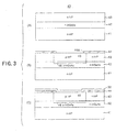
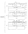
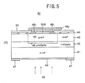
- FIG.3-(A) through FIG.5-(G) show manufacturing steps of a semiconductor photodetection device 40 according to a first example which does not embody the present invention.
- the semiconductor photodetection device 40 is constructed on a substrate 41 of n-type InP, and includes an n-type InGaAs layer 42 formed epitaxially on the substrate 41 and having a carrier concentration of 5.5 x 10 14 cm -3 and a thickness of 2 ⁇ m, and an n-type InP layer 43 formed epitaxially on the InGaAs layer 42 and having a carrier concentration of 3 x 10 15 cm -3 and a thickness of 1.4 ⁇ m.
- the InGaAs layer 42 and InP layer 43 are typically formed by the MOVPE method, but can be formed by other crystal growth technologies such as the MBE method.
- a dielectric protection layer 44 typically made of SiN is formed on the InP layer 43 by the CVD method or other deposition technologies such as sputtering and electron-beam evaporation, and an opening 44A is made in the dielectric protection layer 44 by photolithograpic process.
- a p-type impurity is introduced into the InP layer 43 through the opening 44A by thermal diffusion or ion implantation.
- a p-type region 45 and a p-type InGaAs region 46 are formed corresponding to the opening 44A, in the n-type InP layer 43 and at the top surface of the n-type InGaAs layer 42.
- the p-type impurity may be Zn, Cd, Be or a like substance.
- a dielectric layer 50 made of SiN or a like substance is formed so that it covers the dielectric protection layer 44 and the p-type InP region 45 at the opening 44A. Then the dielectric layer 50 is patterned by photolithographic process as shown in FIG.4-(D) , to form a dielectric layer pattern 50A on an exposed surface of the InP layer 45. As the dielectric layer pattern 50A is formed, a ring-shaped opening 48A is made around the pattern 50A to partially expose the top surface of the p-type InP region 45.
- a ring-shaped contact electrode 48 1 having an Au/Zn/Au layer structure is formed in the ring-shaped opening 48A, by using a vapor deposition process such as resistance heating vacuum vapor deposition or electron-beam evaporation, and a lift-off process. Further, the thus formed ring-shaped contact electrode 48 1 is heated to be alloyed.
- the planarity of the InP layer 43 becomes worse at that area.
- the original planarity of the InP layer 43 is maintained at the area where the dielectric layer pattern 50A is formed, where a light signal which has passed through the InGaAs layer 42 reaches and can be reflected well.
- a resist pattern having an opening exposing the ring-shaped contact electrode 48 1 is made on the dielectric layer 50, a conducting layer made of Ti or Al is deposited on the resist pattern and lifted off, to form a close contact electrode 48 2 which contacts with the ring-shaped contact electrode 48 1 and the dielectric layer pattern 50A.
- the interface between the dielectric layer pattern 50A and the n-type InP layer 43 maintains the original planarity because the dielectric layer pattern 50A does not react with InP.
- a ring-shaped n-type electrode 47 and an antireflection film 49 are formed on the bottom surface of the n-type InP substrate 41.
- the light signal light is partially absorbed by the InGaAs layer 42 and then reflected by the dielectric layer pattern 50A and returned back into the InGaAs layer 42. Because the planarity of the interface between the p-type InP region 45 and the dielectric layer pattern 50A is well maintained, high reflectivity is obtained and optical loss is minimized.
- the close contact electrode 48 2 made of Ti or Al which is well attached by the dielectric layer pattern 50A or the dielectric layer 50, is formed both inside and outside the ring-shaped contact electrode 48 1 , therefore, the total adherence of the electrode including the ring-shaped contact electrode 48 1 and the close contact electrode 48 2 is much improved. As a result, this example can avoid a problem that the contact electrode peels off during manufacturing process such as wire bonding process or mounting process.
- the following table comparatively shows the peeling-off rates of a semiconductor photodetection device according to this example and a conventional device as shown in FIG.2 . These peeling-off rates were obtained by performing the tests 1000 times.
- This table shows that the contact electrode peeled off in more than 80% of the tested conventional devices while the electrode peeled off in less than 1% of the tested photodetection devices according to this example.
- the conductivity types can be reversed from p-type to n-type in this example.
- the semiconductor layers 41-43 are not limited to III-V compound semiconductor materials and may be Si or Ge.
- the close contact electrode 48 2 made of Ti is disposed on the dielectric pattern 50A placed inside the ring-shaped contact electrode 48 1 in the previous example.
- the signal light 52 may not be reflected by the dielectric layer 50A well enough when the reflectivity of the layer 50A is low. In that case, the light coming through the dielectric layer pattern 50A reaches the electrode 48 2 and is absorbed there to degrade the absorption characteristics of the device.
- This second example has a ⁇ (lambda)/4 multiple reflecting layer structure which is mounted on the dielectric layer pattern 50A.
- ⁇ is an incident light wavelength.
- the ⁇ (lambda)/4 multiple reflecting layer structure is formed by laminating SiO 2 layers 50 1 and Si layers 50 2 alternately as shown in FIG.6 .
- the total reflectivity of the laminated SiO 2 layers 50 1 and Si layers 50 2 can be increased to 100% by making each of the optical thicknesses of theses layers set up in 1/4 of the wavelength of the incident light. As a result, it is possible to completely avoid the optical absorption by the Ti close contact electrode 48 2 .
- the dielectric layer pattern 50A itself may have such a multiple layer structure shown in FIG.6 .
- the SiO 2 layers 50 1 and Si layers 50 2 are laminated twice in the example shown in FIG.6 , these layers can be laminated even only once, or three or more times repeatedly. It is preferable to have a SiO 2 layer 50 1 at the top of the laminated reflecting layers 50A in order to stabilize the structure.
- the ⁇ (lambda)/4 multiple reflecting layer can be made of other combination materials such as a SiO 2 layer and a TiO 2 layer.
- a Ge layer can be used instead of a Si layer.
- FIG.7 shows the construction of a close contact electrode 48 2 according to a third example of the present invention.
- the close contact electrode 48 2 of this example has a laminated structure including Ti layer 48 2 A, Pt layer 48 2 B and Au layer 48 2 C.
- the lowermost Ti layer 48 2 A can be well attached to the dielectric pattern 50A.
- the uppermost Au layer 48 2 C lowers the contact resistance and therefore the total resistance of the close contact electrode 48 2 .
- the middle Pt layer 48 2 B interposed between Ti layer 48 2 A and Au layer 48 2 C suppresses interdiffusion between the lowermost layer 48 2 A and the uppermost layer 48 2 C.
- the Ti layer 48 2 A constitutes only a small portion of the electrode 48 2 .
- the high reflective Pt layer 48 2 B and Au layer 48 2 C account for the major portion of the electrode 48 2 , and therefore the absorption of the light coming from the dielectric layer pattern 50A by the Ti layer can be minimized.
- FIG.8 shows the construction of a semiconductor photodetection device 60 according to a fourth example which does not embody the present invention. Those parts corresponding to the parts described previously are designated by the same reference numerals and the description thereof will be omitted.
- the semiconductor photodetection device 60 has a structure similar to that of the previously explained semiconductor photo detection device 40, but is different from the device 40 in that the device 60 has a high reflecting pattern 48 3 as a metal reflecting layer.
- the high reflecting metal layer 48 3 is placed inside the ring-shaped contact electrode 48 1 and covered with the dielectric pattern 50A, and is typically made of Pt, Ni, TiW or TiN.
- the Pt pattern 48 3 is formed on the InP layer 45 inside the opening 44A, and thereafter the dielectric layer 50 is deposited so as to cover the Pt pattern 48 3 .
- the reflectivity of the dielectric pattern 50A having the multiple layer structure shown in FIG.6 is improved as the repeating time of the layers is increased.
- the thickness of the multiple reflecting layer structure 50A is increased at the same time. Accordingly it becomes difficult to form the ring-shaped contact electrode 48 1 in the FIG.4-(E) step, because the ring-shaped opening 48A becomes deeper.
- the reflecting pattern 48 3 itself has high reflectivity, and therefore it is possible to obtain a high reflecting mirror of a small thickness without using the multiple reflecting layer 50A shown in FIG.6 .
- the dielectric layer 50 and 50A thinner, and therefore improve the regularity of the surface of the electrode structure formed on the InP layer 43.
- the step coverage problem when making the contact electrode 48 1 and the close contact electrode 48 2 is alleviated, resulting in improved throughput and reliability in the device manufacturing process.
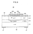
- FIG.9 shows the construction of a semiconductor photodetection device 80 according to a fifth example which does not embody the present invention. Those parts corresponding to the parts described previously are designated by the same reference numerals and the description thereof will be omitted.
- the semiconductor photodetection device 80 has a structure similar to that of the previously explained semiconductor photo detection device 60, but is different from the device 60 in that the high reflecting pattern Pt 48 3 in the device 80 directly contacts with the close contact electrode 48 2 .
- the dielectric pattern 50A is placed only in a ring-shaped area between the high reflecting pattern 48 3 and the ring-shaped contact electrode 48 1 .
- This dielectric layer pattern 50A does not necessarily have to function as a reflecting layer, and therefore can be omitted so that the high reflecting pattern 48 3 contacts with the contact electrode 48 1 .
- the high reflecting pattern 48 3 is made of conductive material such as Pt, Ni, TiW, TiN or similar substance, its electric resistance is low and the frequency response of this device is improved.
- the n-type electrode 47 is formed on the bottom surface of the substrate 41 in this example, it can be alternatively placed on or above the top surface of the n-type InP layer 43 in order to obtain higher frequency response.
- solder bumps may be formed on the close contact electrode 48 2 for flip chip mounting application.
- the pattern 48 3 is preferably made of a transition metal element (so called noble metal) such as Au, Ag or Cu, belonging to group 1B or 2B.
- a transition metal element such as Au, Ag or Cu
- These metals different from other transition metals, have an absorption edge wavelength of less than 0.6 ⁇ m by the total dielectric effect due to inter-band transition and free electrons, and therefore do not absorb light used for optical communication application.
- these metals tend to become thermally diffused into semiconductor layers to create an alloy, and have inferior adhesive characteristics because they have only one or two most outer-shell electrons, and therefore the semiconductor photodetection device using these metals have reliability problem. Further, thermal stress causes other problems that the reflectivity varies and the adhesive strength cannot be maintained when attaching bonding wires or mounting the device on a circuit board.
- the high reflecting pattern 48 3 is made of materials including groups 3A-8A transition metal element such as Ti, having many most outer-shell electrons, in order to prohibit the metal diffusion into semiconductor layers and improve the adhesive strength.
- these metals belonging to groups 3A-8A exhibit strong absorption of light used for optical communication application from the visible region to the far infrared region due to transition in band, and may not achieve the desired high reflectivity.
- material including transition metal elements (such as Au, Ag and Cu) of group 1B or 2B is deposited on the high reflecting pattern 48 3 made of a transition metal element of groups 3A-8A for this example of the present invention.
- the thickness of the layer made of the transition metal elements belonging to groups 3A-8A is selected so as to be less than the absorption length at the signal light wavelength to minimize optical absorption.
- the contact electrode 48 1 is not limited to the ring-shape, and may be of other shapes that partially surround the reflecting pattern 48 3 .
- FIG.10 shows the construction of a surface mounted type avalanche photodiode 100 according to a sixth example which does not embody the present invention, wherein those parts corresponding to the parts described previously are designated by the same reference numerals and the description thereof will be omitted.
- the avalanche photodiode 100 has a general semiconductor layer construction similar to the previously described semiconductor photodetection devices 40-80, and includes an n-type InGaAs optical absorption layer 42 formed on an n-type InP substrate 41 and an n-type InP cap layer 43, and further includes an InGaAsP graded-composition layer 101 doped to n-type between the optical absorption layer 42 and the cap layer 43.
- a p-type region 45 is formed in the cap layer 43, and a p-type guard ring 45G surrounding the p-type region 45 is formed.
- the InP cap layer 43 functions as a photo multiplier layer in this example.
- the avalanche photodiode 100 has a contact trench 100A dug through the InP cap layer 43 all the way to the substrate 41.
- a conductor pattern 100a exists from the bottom of the contact trench 100A to the top surface of the cap layer 43, in order to enable surface mounting.
- a dielectric layer 50 made of SiN or similar substance is formed so as to cover the conductor pattern 100a and the surface of the contact trench 100A.
- a dielectric layer pattern 50A is formed separated from the dielectric layer 50 by a ring-shaped opening 48A (See FIG.4-(D) ).
- a ring-shaped contact electrode 48 1 is formed in the ring-shaped opening 48A.
- a close contact electrode 48 2 typically made of Ti or Al, having excellent adhesive strength to the dielectric layer pattern 50A.
- a contact hall is opened in the dielectric layer 50 to expose the conductor pattern 100a and an n-type electrode 47 is formed so as to connect to the n-type InP substrate 41 via the conductor pattern 100a.
- the dielectric layer pattern 50A maintains the original planarity of the surface of the p-type InP region 45 even after the formation of the close contact elctrode 48 2 . Therefore, light which enters the substrate 41 through an antireflection film 49 and reaches the cap layer 43 without being absorbed by the optical absorption layer 42, can be reflected back to the optical absorption layer 42 with high efficiency and absorbed there.
- the avalanche photodiode according to this example also may utilize the high reflecting layer 48 3 previously explained in the semiconductor photodiode devices 60 and 80.
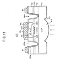
- FIG.11 shows the construction of a surface mounted type avalanche photodiode 110 according to a seventh example which does not embody the present invention, wherein those parts corresponding to the parts described previously are designated by the same reference numerals and the description thereof will be omitted.
- the avalanche photodiode 110 has a lens-like condenser portion 41L formed at the bottom surface of an InP substrate 41. Therefore, a light signal incident to the device is efficiently condensed on the photodetection structure.
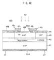
- FIG.12 shows the construction of a semiconductor photodetection device 120 of a type that receives incoming optical signals at a top surface side according to an eighth example which does not embody the present invention, wherein those parts corresponding to the parts described previously are designated by the same reference numerals and the description thereof will be omitted.
- the surface-incident type semiconductor photodetection device 120 has a general construction similar to the semiconductor photodetection device 40 shown in FIG.5 , but the dielectric layer 50 and the dielectric layer pattern 50A are replaced by an antireflection film 49A, 49B, and an opening 48W is made in a closed contact electrode 48 2 to expose the antireflection film 49A.
- a high reflecting dielectric layer pattern 50A is formed on the bottom surface of a substrate 41, and an n-type electrode 47 is formed at the bottom surface of the substrate 41 so as to cover the high reflecting layer pattern 50A.
- an incident light 52 passes through the antireflection film 49A after passing through a window 48W in the close contact electrode 48 2 , and is then absorbed by an optical absorption layer 42.
- a part of the incident light beam which has not been absorbed is reflected by the high reflecting layer 50A formed on the bottom surface of the substrate 41 and returned to the optical absorption layer 42. Because the dielectric layer 50A is formed between the bottom surface of the substrate 41 and the n-type electrode 47, no alloy is created between them, and therefore an excellent reflecting surface is maintained there.
- FIG.13 is an enlarged cross-sectional view of a photodetection area of a substrate-incident type semiconductor photodetection device 130 according to a first embodiment of the present invention. A semiconductor substrate and electrodes are not shown in FIG.13 .
- the semiconductor photodetection device 130 includes an epitaxially formed n-type InP layer 132 having a carrier concentration of 2 x 10 17 cm -3 and a thickness of 1.5 ⁇ m, an n-type InGaAs optical absorption layer 133 formed epitaxially on the InP layer 132 and having a carrier concentration of 5.5 x 10 14 cm -3 and a thickness of 2 ⁇ m, and an n-type InP layer 134 formed epitaxially on the optical absorption layer 133 and having a carrier concentration of 6 x 10 15 cm -3 and a thickness of 1.5 ⁇ m.
- a p-type region 134A including Zn, Cd, Be or similar substance is formed in the InP layer 134 so as to reach the optical absorption layer 133.
- a insulating layer 135 of SiN layer or similar substance is formed typically by the CVD method on the InP layer 134 and an opening is made in the insulating layer 135 to expose the p-type region 134A.
- a SiN or SiO 2 dielectric layer 136 having an optical thickness set up in 1/4 of a signal light wavelength is formed typically by the CVD method on the insulating layer 135.
- the p-type region 134A is formed by introducing p-type impurity atoms through the opening in insulating layer 135 and thermally diffusing them.
- Dielectric layer 136 is then patterned, and a dielectric layer 135A is formed as a mirror on the p-type region 134A, separated from the dielectric layer 136 by a ring-shaped trench.
- a ring-shaped Au/Zn/Au electrode pattern 137 ohmic-contacting with the p-type region 134A, by the lifting-off method.
- a ring-shaped barrier pattern 138 is formed on the ring-shaped Au/Zn/An electrode pattern 137 by laminating Ti and Pt layers in turn.
- An Au pillar 139 is formed on the ring-shaped barrier pattern 138 by plating and lifting-off method, so as to contact with the dielectric pattern 135A.
- a bump electrode 140 of Au/Sn alloy metal is formed on the Au pillar 139.
- the ring-shaped electrode pattern 137 ohmic-contacts with p-type diffusion region 134A and the planarity of their interface gets worse.
- the interface between the dielectric mirror pattern 135A and the p-type diffusion region 134A is planar providing an area, where the light signal is well reflected.
- the Au pillar 139 functions a refection mirror together with the dielectric mirror pattern 135A.
- the Au pillar 139 does not adhere well to the dielectric mirror pattern 135A, but adheres well to the ring-shaped barrier pattern 138 and therefore the Au pillar 139 is prevented from peeling off.
- the Ti atom has many most outer-shell electrons, and is strongly bonded to other elements.
- Pt functions as a diffusion barrier, which inhibits Au in the Au pillar 139 from diffusing into the p-type diffusion region 134A. In this structure, stable reflectivity is obtained even when the semiconductor photodetection device 130 suffers thermal stress.
- a TiW layer or TiN layer can be used as the ring-shaped barrier pattern 138, instead of Ti/Pt laminated layers.
- another transition metal element belonging to group 1B or 2B such as Ag or Cu or group 3B such as Al can be used for the pillar 139.
- FIG.14 shows the results of a chip bonding strength test performed on the semiconductor photodetection device 130.
- ⁇ (a square) represents the result of testing the conventional semiconductor photodetection device
- ⁇ (a solid circle) represents the result of testing the semiconductor photodetection device 130.
- FIG.15 shows the construction of a semiconductor photodetection device 150 according to a ninth example, not embodying the invention, wherein those parts corresponding to the parts described previously are designated by the same reference numerals and the description thereof will be omitted.
- a Ti close contact layer 138A is interposed between a ring-shaped barrier layer pattern 138 and an Au pillar 139 and between a dielectric mirror pattern 135A and the Au pillar 139. This Ti close contact layer makes the bonding strength of the semiconductor photodetection device 150 stronger.
- the Ti layer absorbs light at the operational wavelength of the semiconductor photodetection device 150. Therefore, the thickness of the Ti close contact layer 138A is arranged to be thinner than the absorption length (the inverse number of absorption coefficient of the Ti layer.
- FIG.16 shows the relationships between the thicknesses and reflectivities at 1550nm and 1620nm wavelenghs.
- the reflectivity decreases as the Ti layer gets thicker.
- the thickness of the Ti layer should be less than 40nm in order to obtain a desirable reflectivity that is equal to or better than the reflectivity (60%) of a conventional reflection mirror having a laminated 100nm Ti layer and 215nm SiN layer.
- the thickness of the close contact layer 138A is preferably less than 40nm.
- a close contact layer 138A having a thickness of 30nm gives a reflectivity higher than prior devices.
- FIG.17 shows the construction of a semiconductor photodetection device 160 according to a tenth example of the present invention, wherein those parts corresponding to the parts described previously are designated by the same reference numerals and the description thereof will be omitted.
- a dielectric layer mirror pattern 50A and a dielectric layer pattern 50B are formed on the bottom surface of a substrate 41 by patterning dielectric layers thereon.
- a ring-shaped Au/Ge/Au ohmic electrode 51 is formed in a ring-shaped groove between the dielectric layer mirror pattern 50A and the dielectric layer pattern 50B.
- a ring-shaped Ti/Pt barrier electron pattern 52 is formed so as to cross-link the dielectric layer mirror pattern 50A and the dielectric layer pattern 50B and to directly contact with the ring-shaped ohmic electrode 51 interposed between them.
- An Au electrode 47 is formed on the barrier electrode pattern 52 so as to contact with the dielectric reflection pattern 50A through an opening made in the barrier electrode pattern 52.
- a bump electrode 53 for mounting purposes is formed on the Au electrode 47.
- the electrode 47 may be made of transition metal belonging to group 1B or 2B such as Ag or Cu, which absorbs less light.
- An n-type InP buffer layer 41A is interposed between the InP substrate 41 and the InGaAs optical absorption layer 42.
- incident light comes through a dielectric layer 49A into the substrate 41, and is reflected by the dielectric mirror pattern 50A and absorbed by an optical absorption layer 42.
- the Ti/Pt barrier electrode 52 is formed on the dielectric layer patterns 50A, 50B and connected to the Au electrode 47, the weak adhesion between the Au electrode 47 and the dielectric layer mirror 50A is compensated for, and therefore the semiconductor photodetection device 160 can be reliably mounted on a circuit board. Because there is no ohmic contact between the dielectric layer mirror pattern 50A and the substrate 41, high reflectivity is attained.
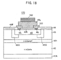
- FIG.18 is an enlarged cross-sectional view of a photodetection area of a surface mounting type avalanche photodiode 170 according to a second embodiment of the present invention, wherein those parts corresponding to the parts described previously are designated by the same reference numerals and the description thereof will be omitted.
- the avalanche photodiode 170 has a structure similar to that of the previously explained avalanche photodiode 100 shown in FIG.10 , but is different in the following ways.
- An electrode 48 2 is made of transition metal belonging to group 1B or 2B such as Au, Ag or Cu which absorbs less light.
- a Ti/Pt barrier electrode 161 is interposed between the ohmic electrode 48 1 and the Au layer 48 2 .
- An Au/Sn bump for mounting purposes is formed on the electrode 48 2 .
- An n-type InP buffer layer 41A is interposed between a substrate (not shown) and an InGaAs layer 42.
- the avalanche photodiode 170 can be reliably flip-chip-mounted on a circuit board with high strength.
- a Ti layer that absorbs light is used only for the barrier electrode 161, and therefor the reflectivity of the reflecting region including the dielectric layer mirror 49A is not lowered.
- Each embodiment and example explained above is a planar type device in which p-type semiconductors are made by diffusing impurities.
- the present invention can be applied to a mesa-type device.
- Conducting types can be reversed from p-type to n-type in each embodiment/example above.
- III-V compound semiconductor the present invention can be applied to other types of semiconductors such as Si or Ge.
- the present invention as set forth above, it becomes possible to obtain high adhesive strength of the electrodes including the contact electrode and the close contact electrode, and avoid the contact electrode peeling-off problem during the manufacturing process or packaging and mounting processes including a wire bonding process. Further, it becomes possible to planarize the light reflection surface and improve the reflectivity. Further, in the case of using a metal layer as a reflection mirror, the thickness of layers becomes small. As a result, the step coverage problem when forming electrodes is alleviated and the throughput and reliability when manufacturing this device is much improved.
Landscapes
- Light Receiving Elements (AREA)
Description
- The present invention generally relates to optical semiconductor devices and more particularly to a semiconductor photodetection device used especially for fiber optics communication system.
-
FIG.1 shows in general the structure of a conventionalsemiconductor photodetection device 10 of the type that receives incoming optical signal at a substrate surface side. - Referring to
FIG.1 , thesemiconductor photodetection device 10 is constructed on asubstrate 11 of n-type InP, and includes a layer structure having an n-type InGaAsoptical absorption layer 12 with low carrier concentration formed on thesubstrate 11 and acap layer 13 of n-type InP formed on thelayer 12. A p-type InGaAs region 16 and p-type InP region 15 are formed in the InGaAsoptical absorption layer 12 and the n-typeInP cap layer 13 by introducing a p-type impurity through an opening, which has been patterned in adielectric protection layer 14 formed on thecap layer 13. An n-type electrode 17 is formed on the n-type InP substrate 11 and a p-type contact electrode 18 is formed on the p-type InP region 15, respectively. In the n-type electrode 17 is formed an optical window, through which an optical signal passes. In this illustrated embodiment, anantireflection film 19 is formed at the optical window on thesubstrate 11. - In operation of the
photodetection device 10 shown inFIG. 1 , a reverse bias voltage is applied between theelectrodes substrate 11 through the optical window. Because thesubstrate InP layer 11 is transparent to the light having the above wavelength, the incident signal light reaches the InGaAsoptical absorption layer 12 without being absorbed by thesubstrate 11, and there occurs excitation of photocarriers in theoptical absorption layer 12. - The frequency response of such a semiconductor photodetection device is generally determined by a time constant CR and a transit time of the carrier excited by the incident light, where C is a capacitance and R is an internal resistance of the device. In order to improve the frequency response of the
semiconductor photodetection device 10, the time constant needs to be shortened and the carrier transit time also needs to be shortened. Because the carrier transit time increases proportionally to the thickness of the InGaAsoptical absorption layer 12, it should be reduced in thickness, as much as possible in order to shorten the carrier transit time to improve the frequency response. - However, if the thickness of the InGaAs
optical absorption layer 12 is reduced with the aim of achieving high speed, theoptical absorption layer 12 can not absorb the incident light sufficiently, which degrades the quantum efficiency of the optical absorption. - Thus, because there exists a trade-off relationship between the frequency response and the quantum efficiency, it is difficult to obtain the optimum thickness of the InGaAs
optical absorption layer 12 when designing semiconductor photodetection devices requiring high-speed response. - In order to solve this efficiency problem, in the conventional
semiconductor photodetection device 10 of the substrate-side incident type shown inFIG. 1 , the signal light that has not been absorbed by theoptical absorption layer 12 is reflected by the p-type contact electrode 18 and re-introduced into theoptical absorption layer 12 through theInP cap layer 13 to avoid the reduction in the quantum efficiency. - In the
semiconductor photodetection device 10 shown inFIG. 1 , while a metal layer constituting thecontact electrode 18 is vapor-deposited on the n-typeInP cap layer 13, heat resulting from the vapor-deposition forms an alloy metal layer at the interface between theInP cap layer 13 and themetal contact electrode 18. As a result, the planarity of the interface between theInP cap layer 13 and thecontact electrode 18 is degraded. This degradation of planarity significantly lowers the reflectivity of the interface and reduces the amount of the signal light reflected by the interface, and therefore the signal light is mostly scattered by the interface and cannot be absorbed well enough in the InGaAsoptical absorption layer 12. Consequently, the quantum efficiency is lowered and the amount of light returning from thephotodetection device 10 to an optical fiber is increased, resulting in lower the transmission characteristics of fiber optics communication system. - In order to deal with the above mentioned problem, there has been a proposal, in Japanese Laid-Open Patent Publication
5-218488 dielectric layer 20 be interposed between thecap layer 13 and thecontact electrode 18 as shown inFIG. 2 , and would inhibit the alloying reaction between the metal layer of thecontact electrode 18 and the InP layer of thecap layer 13. Similar or the same parts inFIG. 2 corresponding to the previously described parts inFIG. 1 are designated by the same reference numerals and the description thereof will be omitted. - This conventional structure of the substrate side incident type semiconductor photodetection device shown in Japanese Laid-Open Patent Publication
5-218488 contact electrode 18 and theInP cap layer 13 is reduced because of thedielectric layer 20, and the adherence between the metal layer of thecontact electrode 18 and thedielectric layer 20 is not strong enough. Therefore, there has been a problem that thecontact electrode 18 peels off during the manufacturing process, wire bonding process or flip chip mounting process. -
JP 01 1264273A EP0343970A2 each disclose a semiconductor photodetection device, comprising a semiconductor structure including an optical absorption layer having a photo-incidence surface on a first side thereof, a dielectric reflecting layer formed on a second side of the semiconductor structure opposite to the first side, and a contact electrode surrounding the dielectric reflecting layer and contacting with the semiconductor structure. - Accordingly, it is a general object of the present invention to provide a novel and useful semiconductor photodetection device wherein the foregoing problems are eliminated.
- Another and more specific object of the present invention is to provide a reliable semiconductor photodetection device having high speed response and high efficiency.
- According to the present invention there is provided a semiconductor photodetection device, comprising: a semiconductor structure including an optical absorption layer having a photo-incidence surface on a first side thereof; a dielectric reflecting layer formed on a second side of the semiconductor structure opposite to the first side; and a contact electrode surrounding the dielectric reflecting layer and contacting with the semiconductor structure; characterised by: a barrier electrode formed on the periphery of the dielectric reflecting layer and contacting with the contact electrode; and a reflecting electrode covering the dielectric reflecting layer and contacting with the barrier electrode and the dielectric reflecting layer; wherein said barrier electrode has a larger area than the contact electrode.
- It is preferable to form the semiconductor photodetection device so that the dielectric reflecting layer is made of fluoride, oxide or nitride including one or more atoms selected from the group consisting of Si, Al, Mg, Ti, Zr and Ta. Further, it is preferable to form the semiconductor photodetection device so that the contact electrode is a ring shape. Further, it is preferable to form the semiconductor photodetection device so that the contact electrode is formed partially surrounding the dielectric reflecting layer. Further, it is preferable to form the semiconductor photodetection device so that the semiconductor structure is mounted on a semiconductor substrate and the photo-incidence surface is placed on the substrate side of the semiconductor structure. Further, it is preferable to form the semiconductor photodetection device so that the semiconductor structure further includes a carrier-multiplier layer, and the semiconductor photodetection device is an avalanche photodiode.
- According to the present invention, it becomes possible to improve the total adherence of the electrode by having a dielectric reflecting layer inside the contact electrode and by having a close contact electrode mounted on the dielectric protection layer outside of the contact electrode, wherein the close contact electrode is made of high adhesive metal. As a result, it becomes possible to avoid a problem that the contact electrode peels off during manufacturing process, wire bonding process or flip chip mounting process. Further, it becomes possible to improve the planarity and reflectivity of a reflecting surface by having a metal reflecting layer inside the contact electrode wherein the metal reflecting layer has low reactivity with a semiconductor layer. Further, it becomes possible to obtain a high reflective mirror with thin layers by using a metal layer as a reflective layer. As a result, it becomes possible to improve step coverage, throughput and reliability of semiconductor photodetection device.
- Other objects and further features of the present invention will become apparent from the following detailed description when read in conjunction with the attached drawings.
-
-
FIG.1 is a cross-sectional view showing the construction of a conventional semiconductor photodetection device; -
FIG.2 is a cross-sectional view showing the construction of another conventional semiconductor photodetection device; -
FIG.3 shows manufacturing steps of a semiconductor photodetection device according to a first example which does not embody the present invention but is useful for understanding it; -
FIG.4 shows subsequent manufacturing steps of the semiconductor photodetection device ofFig. 3 ; -
FIG.5 is a cross-sectional view showing the construction of the semiconductor photodetection device ofFig. 3 ; -
FIG.6 is a cross-sectional view showing a part of a semiconductor photodetection device according to a second example which does not embody the present invention but is useful for understanding it; -
FIG.7 is a cross-sectional view showing a part of a semiconductor photodetection device according to a third example which does not embody the present invention but is useful for understanding it; -
FIG.8 is a cross-sectional view showing the construction of a semiconductor photodetection device according to a fourth example which does not embody the present invention but is useful for understanding it; -
FIG.9 is a cross-sectional view showing the construction of a semiconductor photodetection device according to a fifth example which does not embody the present invention but is useful for understanding it; -
FIG. 10 is a cross-sectional view showing the construction of an avalanche photodiode according to a sixth example which does not embody the present invention but is useful for understanding it; -
FIG. 11 is a cross-sectional view showing the construction of an avalanche photodiode according to a seventh example which does not embody the present invention but is useful for understanding it; -
FIG. 12 is a cross-sectional view showing the construction of a semiconductor photodetection device according to an eighth example which does not embody the present invention but is useful for understanding it; -
FIG. 13 is a cross-sectional view showing the construction of a photodetection area of a semiconductor photodetection device according to a first embodiment of the present invention; -
FIG. 14 is a chart showing bonding strengths of the semiconductor photodetection device shown inFIG. 9 ; -
FIG. 15 is a cross-sectional view showing the construction of a photodetection area of a semiconductor photodetection device according to a ninth example which does not embody the present invention but is useful for understanding it; -
FIG. 16 is a chart showing the relationship between reflectivities and thicknesses of a Ti close contact layer of the semiconductor photodetection device shown inFIG. 15 ; -
FIG. 17 is a cross-sectional view showing the construction of a semiconductor photodetection device according to a tenth example which does not embody the present invention but is useful for understanding it; and -
FIG. 18 is a cross-sectional view showing the construction of a photodetection area of a semiconductor photodetection device according to a second embodiment of the present invention. -
FIG.3-(A) through FIG.5-(G) show manufacturing steps of asemiconductor photodetection device 40 according to a first example which does not embody the present invention. - Referring to
FIG.3-(A) , thesemiconductor photodetection device 40 is constructed on asubstrate 41 of n-type InP, and includes an n-type InGaAs layer 42 formed epitaxially on thesubstrate 41 and having a carrier concentration of 5.5 x 1014 cm-3 and a thickness of 2µm, and an n-type InP layer 43 formed epitaxially on theInGaAs layer 42 and having a carrier concentration of 3 x 1015 cm-3 and a thickness of 1.4µm. The InGaAslayer 42 andInP layer 43 are typically formed by the MOVPE method, but can be formed by other crystal growth technologies such as the MBE method. - Referring to
FIG.3-(B) , adielectric protection layer 44 typically made of SiN is formed on theInP layer 43 by the CVD method or other deposition technologies such as sputtering and electron-beam evaporation, and an opening 44A is made in thedielectric protection layer 44 by photolithograpic process. A p-type impurity is introduced into theInP layer 43 through theopening 44A by thermal diffusion or ion implantation. As a result, a p-type region 45 and a p-type InGaAs region 46 are formed corresponding to theopening 44A, in the n-type InP layer 43 and at the top surface of the n-type InGaAs layer 42. The p-type impurity may be Zn, Cd, Be or a like substance. - Referring to
FIG.3-(C) , adielectric layer 50 made of SiN or a like substance is formed so that it covers thedielectric protection layer 44 and the p-type InP region 45 at theopening 44A. Then thedielectric layer 50 is patterned by photolithographic process as shown inFIG.4-(D) , to form adielectric layer pattern 50A on an exposed surface of theInP layer 45. As thedielectric layer pattern 50A is formed, a ring-shapedopening 48A is made around thepattern 50A to partially expose the top surface of the p-type InP region 45. - In a subsequent step shown in
FIG.4-(E) , a ring-shaped contact electrode 481 having an Au/Zn/Au layer structure is formed in the ring-shapedopening 48A, by using a vapor deposition process such as resistance heating vacuum vapor deposition or electron-beam evaporation, and a lift-off process. Further, the thus formed ring-shaped contact electrode 481 is heated to be alloyed. - Because an alloy layer is made at a ring-shaped interface area between the p-
type InP region 45 and the ring-shaped contact electrode 481 due to the heat process, the planarity of theInP layer 43 becomes worse at that area. However, the original planarity of theInP layer 43 is maintained at the area where thedielectric layer pattern 50A is formed, where a light signal which has passed through theInGaAs layer 42 reaches and can be reflected well. - Referring to
FIG.4-(F) , a resist pattern having an opening exposing the ring-shaped contact electrode 481 is made on thedielectric layer 50, a conducting layer made of Ti or Al is deposited on the resist pattern and lifted off, to form a close contact electrode 482 which contacts with the ring-shaped contact electrode 481 and thedielectric layer pattern 50A. - In the above steps, in spite of the heating alloying process of the contact electrode 481, the interface between the
dielectric layer pattern 50A and the n-type InP layer 43 maintains the original planarity because thedielectric layer pattern 50A does not react with InP. - Referring to
FIG.5-(G) , a ring-shaped n-type electrode 47 and anantireflection film 49 are formed on the bottom surface of the n-type InP substrate 41. When a signal light is introduced into thesubstrate 41 through theantireflection film 49, the light signal light is partially absorbed by theInGaAs layer 42 and then reflected by thedielectric layer pattern 50A and returned back into theInGaAs layer 42. Because the planarity of the interface between the p-type InP region 45 and thedielectric layer pattern 50A is well maintained, high reflectivity is obtained and optical loss is minimized. - In this example, the close contact electrode 482 made of Ti or Al which is well attached by the
dielectric layer pattern 50A or thedielectric layer 50, is formed both inside and outside the ring-shaped contact electrode 481, therefore, the total adherence of the electrode including the ring-shaped contact electrode 481 and the close contact electrode 482 is much improved. As a result, this example can avoid a problem that the contact electrode peels off during manufacturing process such as wire bonding process or mounting process. - The following table comparatively shows the peeling-off rates of a semiconductor photodetection device according to this example and a conventional device as shown in
FIG.2 . These peeling-off rates were obtained by performing the tests 1000 times.Device Peeling-off rate Conventional device >80% This example <1% - This table shows that the contact electrode peeled off in more than 80% of the tested conventional devices while the electrode peeled off in less than 1% of the tested photodetection devices according to this example.
- As mentioned above, it is possible to use Al instead of Ti as the close contact electrode 482 in this example. And it is also possible to use a fluoride layer or an oxide layer of Si, Al, Mg, Ti, Zr, Ta or similar substance instead of a SiN layer as the
dielectric layer 50A. - The conductivity types can be reversed from p-type to n-type in this example. The semiconductor layers 41-43 are not limited to III-V compound semiconductor materials and may be Si or Ge.
- The close contact electrode 482 made of Ti is disposed on the
dielectric pattern 50A placed inside the ring-shaped contact electrode 481 in the previous example. - Even though the interface between the p-
type InP region 45 and thedielectric pattern 50A is planar, thesignal light 52 may not be reflected by thedielectric layer 50A well enough when the reflectivity of thelayer 50A is low. In that case, the light coming through thedielectric layer pattern 50A reaches the electrode 482 and is absorbed there to degrade the absorption characteristics of the device. - This second example has a λ(lambda)/4 multiple reflecting layer structure which is mounted on the
dielectric layer pattern 50A. λ is an incident light wavelength. The λ(lambda)/4 multiple reflecting layer structure is formed by laminating SiO2 layers 501 and Si layers 502 alternately as shown inFIG.6 . The total reflectivity of the laminated SiO2 layers 501 and Si layers 502 can be increased to 100% by making each of the optical thicknesses of theses layers set up in 1/4 of the wavelength of the incident light. As a result, it is possible to completely avoid the optical absorption by the Ti close contact electrode 482. - Alternatively, the
dielectric layer pattern 50A itself may have such a multiple layer structure shown inFIG.6 . Although the SiO2 layers 501 and Si layers 502 are laminated twice in the example shown inFIG.6 , these layers can be laminated even only once, or three or more times repeatedly. It is preferable to have a SiO2 layer 501 at the top of the laminated reflectinglayers 50A in order to stabilize the structure. The λ(lambda)/4 multiple reflecting layer can be made of other combination materials such as a SiO2 layer and a TiO2 layer. And a Ge layer can be used instead of a Si layer. -
FIG.7 shows the construction of a close contact electrode 482 according to a third example of the present invention. - Referring to
FIG.7 , the close contact electrode 482 of this example has a laminated structure includingTi layer 482A, Pt layer 482B and Au layer 482C. Thelowermost Ti layer 482A can be well attached to thedielectric pattern 50A. On the other hand, the uppermost Au layer 482C lowers the contact resistance and therefore the total resistance of the close contact electrode 482. Further, the middle Pt layer 482B interposed betweenTi layer 482A and Au layer 482C suppresses interdiffusion between thelowermost layer 482A and the uppermost layer 482C. - In this structure shown in
FIG.7 , theTi layer 482A constitutes only a small portion of the electrode 482. The high reflective Pt layer 482B and Au layer 482C account for the major portion of the electrode 482, and therefore the absorption of the light coming from thedielectric layer pattern 50A by the Ti layer can be minimized. -
FIG.8 shows the construction of asemiconductor photodetection device 60 according to a fourth example which does not embody the present invention. Those parts corresponding to the parts described previously are designated by the same reference numerals and the description thereof will be omitted. - Referring to
FIG.8 , thesemiconductor photodetection device 60 has a structure similar to that of the previously explained semiconductorphoto detection device 40, but is different from thedevice 40 in that thedevice 60 has a high reflecting pattern 483 as a metal reflecting layer. The high reflecting metal layer 483 is placed inside the ring-shaped contact electrode 481 and covered with thedielectric pattern 50A, and is typically made of Pt, Ni, TiW or TiN. - In actual manufacturing process of the
semiconductor photodetection device 60 as shown inFIG. 8 , after the formation of the p-type InP region 45 in the step shown inFIG.3-(B) , the Pt pattern 483 is formed on theInP layer 45 inside theopening 44A, and thereafter thedielectric layer 50 is deposited so as to cover the Pt pattern 483. - The reflectivity of the
dielectric pattern 50A having the multiple layer structure shown inFIG.6 is improved as the repeating time of the layers is increased. However, the thickness of the multiple reflectinglayer structure 50A is increased at the same time. Accordingly it becomes difficult to form the ring-shaped contact electrode 481 in theFIG.4-(E) step, because the ring-shapedopening 48A becomes deeper. On the other hand, according to this example, the reflecting pattern 483 itself has high reflectivity, and therefore it is possible to obtain a high reflecting mirror of a small thickness without using the multiple reflectinglayer 50A shown inFIG.6 . - According to this example, it is possible to make the
dielectric layer InP layer 43. As a result, the step coverage problem when making the contact electrode 481 and the close contact electrode 482 is alleviated, resulting in improved throughput and reliability in the device manufacturing process. -
FIG.9 shows the construction of asemiconductor photodetection device 80 according to a fifth example which does not embody the present invention. Those parts corresponding to the parts described previously are designated by the same reference numerals and the description thereof will be omitted. - Referring to
FIG.9 , thesemiconductor photodetection device 80 has a structure similar to that of the previously explained semiconductorphoto detection device 60, but is different from thedevice 60 in that the high reflecting pattern Pt 483 in thedevice 80 directly contacts with the close contact electrode 482. Thedielectric pattern 50A is placed only in a ring-shaped area between the high reflecting pattern 483 and the ring-shaped contact electrode 481. - This
dielectric layer pattern 50A does not necessarily have to function as a reflecting layer, and therefore can be omitted so that the high reflecting pattern 483 contacts with the contact electrode 481. - In this example, because the high reflecting pattern 483 is made of conductive material such as Pt, Ni, TiW, TiN or similar substance, its electric resistance is low and the frequency response of this device is improved.
- Although the n-
type electrode 47 is formed on the bottom surface of thesubstrate 41 in this example, it can be alternatively placed on or above the top surface of the n-type InP layer 43 in order to obtain higher frequency response. In this case, solder bumps may be formed on the close contact electrode 482 for flip chip mounting application. - Considerations of the material for the high reflecting pattern 483 will be given below.
- In order to improve the reflectivity of the reflecting pattern 483 to nearly 100%, the pattern 483 is preferably made of a transition metal element (so called noble metal) such as Au, Ag or Cu, belonging to group 1B or 2B. These metals, different from other transition metals, have an absorption edge wavelength of less than 0.6µm by the total dielectric effect due to inter-band transition and free electrons, and therefore do not absorb light used for optical communication application.
- On the other hand, these metals tend to become thermally diffused into semiconductor layers to create an alloy, and have inferior adhesive characteristics because they have only one or two most outer-shell electrons, and therefore the semiconductor photodetection device using these metals have reliability problem. Further, thermal stress causes other problems that the reflectivity varies and the adhesive strength cannot be maintained when attaching bonding wires or mounting the device on a circuit board.
- For this example, the high reflecting pattern 483 is made of materials including groups 3A-8A transition metal element such as Ti, having many most outer-shell electrons, in order to prohibit the metal diffusion into semiconductor layers and improve the adhesive strength. On the other hand, these metals belonging to groups 3A-8A exhibit strong absorption of light used for optical communication application from the visible region to the far infrared region due to transition in band, and may not achieve the desired high reflectivity.
- In consideration of these problems, material including transition metal elements (such as Au, Ag and Cu) of group 1B or 2B is deposited on the high reflecting pattern 483 made of a transition metal element of groups 3A-8A for this example of the present invention. The thickness of the layer made of the transition metal elements belonging to groups 3A-8A is selected so as to be less than the absorption length at the signal light wavelength to minimize optical absorption.
- The contact electrode 481 is not limited to the ring-shape, and may be of other shapes that partially surround the reflecting pattern 483.
- Although the above examples were explained using a substrate side incident type of photodetection device, the principles explained can be applied to a surface incident type of photodetection device.
-
FIG.10 shows the construction of a surface mountedtype avalanche photodiode 100 according to a sixth example which does not embody the present invention, wherein those parts corresponding to the parts described previously are designated by the same reference numerals and the description thereof will be omitted. - Referring to
FIG.10 , theavalanche photodiode 100 has a general semiconductor layer construction similar to the previously described semiconductor photodetection devices 40-80, and includes an n-type InGaAsoptical absorption layer 42 formed on an n-type InP substrate 41 and an n-typeInP cap layer 43, and further includes an InGaAsP graded-composition layer 101 doped to n-type between theoptical absorption layer 42 and thecap layer 43. A p-type region 45 is formed in thecap layer 43, and a p-type guard ring 45G surrounding the p-type region 45 is formed. TheInP cap layer 43 functions as a photo multiplier layer in this example. - The
avalanche photodiode 100 according to this example has acontact trench 100A dug through theInP cap layer 43 all the way to thesubstrate 41. Aconductor pattern 100a exists from the bottom of thecontact trench 100A to the top surface of thecap layer 43, in order to enable surface mounting. - On the surface of the
InP cap layer 43, adielectric layer 50 made of SiN or similar substance is formed so as to cover theconductor pattern 100a and the surface of thecontact trench 100A. Adielectric layer pattern 50A is formed separated from thedielectric layer 50 by a ring-shapedopening 48A (SeeFIG.4-(D) ). A ring-shaped contact electrode 481 is formed in the ring-shapedopening 48A. - Further, on the
dielectric layer pattern 50A is formed a close contact electrode 482 typically made of Ti or Al, having excellent adhesive strength to thedielectric layer pattern 50A. - A contact hall is opened in the
dielectric layer 50 to expose theconductor pattern 100a and an n-type electrode 47 is formed so as to connect to the n-type InP substrate 41 via theconductor pattern 100a. - Also in this avalanche photodiode, the
dielectric layer pattern 50A maintains the original planarity of the surface of the p-type InP region 45 even after the formation of the close contact elctrode 482. Therefore, light which enters thesubstrate 41 through anantireflection film 49 and reaches thecap layer 43 without being absorbed by theoptical absorption layer 42, can be reflected back to theoptical absorption layer 42 with high efficiency and absorbed there. - The avalanche photodiode according to this example also may utilize the high reflecting layer 483 previously explained in the
semiconductor photodiode devices -
FIG.11 shows the construction of a surface mountedtype avalanche photodiode 110 according to a seventh example which does not embody the present invention, wherein those parts corresponding to the parts described previously are designated by the same reference numerals and the description thereof will be omitted. - Referring to
FIG.11 , theavalanche photodiode 110 has a lens-like condenser portion 41L formed at the bottom surface of anInP substrate 41. Therefore, a light signal incident to the device is efficiently condensed on the photodetection structure. - Other features of this example are the same as those of the previous example and the description thereof will be omitted.
-
FIG.12 shows the construction of asemiconductor photodetection device 120 of a type that receives incoming optical signals at a top surface side according to an eighth example which does not embody the present invention, wherein those parts corresponding to the parts described previously are designated by the same reference numerals and the description thereof will be omitted. - Referring to
FIG.12 , the surface-incident typesemiconductor photodetection device 120 has a general construction similar to thesemiconductor photodetection device 40 shown inFIG.5 , but thedielectric layer 50 and thedielectric layer pattern 50A are replaced by anantireflection film opening 48W is made in a closed contact electrode 482 to expose theantireflection film 49A. - In the surface-incident type
semiconductor photodetection device 120 shown inFIG.12 , a high reflectingdielectric layer pattern 50A is formed on the bottom surface of asubstrate 41, and an n-type electrode 47 is formed at the bottom surface of thesubstrate 41 so as to cover the high reflectinglayer pattern 50A. - In the operation of the
semiconductor photodetection device 120, an incident light 52 passes through theantireflection film 49A after passing through awindow 48W in the close contact electrode 482, and is then absorbed by anoptical absorption layer 42. A part of the incident light beam which has not been absorbed is reflected by the high reflectinglayer 50A formed on the bottom surface of thesubstrate 41 and returned to theoptical absorption layer 42. Because thedielectric layer 50A is formed between the bottom surface of thesubstrate 41 and the n-type electrode 47, no alloy is created between them, and therefore an excellent reflecting surface is maintained there. -
FIG.13 is an enlarged cross-sectional view of a photodetection area of a substrate-incident typesemiconductor photodetection device 130 according to a first embodiment of the present invention. A semiconductor substrate and electrodes are not shown inFIG.13 . - Referring to
FIG.13 , thesemiconductor photodetection device 130 includes an epitaxially formed n-type InP layer 132 having a carrier concentration of 2 x 1017 cm-3 and a thickness of 1.5µm, an n-type InGaAsoptical absorption layer 133 formed epitaxially on theInP layer 132 and having a carrier concentration of 5.5 x 1014 cm-3 and a thickness of 2µm, and an n-type InP layer 134 formed epitaxially on theoptical absorption layer 133 and having a carrier concentration of 6 x 1015 cm-3 and a thickness of 1.5µm. A p-type region 134A including Zn, Cd, Be or similar substance is formed in theInP layer 134 so as to reach theoptical absorption layer 133. - A insulating
layer 135 of SiN layer or similar substance is formed typically by the CVD method on theInP layer 134 and an opening is made in the insulatinglayer 135 to expose the p-type region 134A. A SiN or SiO2dielectric layer 136 having an optical thickness set up in 1/4 of a signal light wavelength is formed typically by the CVD method on the insulatinglayer 135. The p-type region 134A is formed by introducing p-type impurity atoms through the opening in insulatinglayer 135 and thermally diffusing them. -
Dielectric layer 136 is then patterned, and adielectric layer 135A is formed as a mirror on the p-type region 134A, separated from thedielectric layer 136 by a ring-shaped trench. In the ring-shaped trench is formed a ring-shaped Au/Zn/Au electrode pattern 137 ohmic-contacting with the p-type region 134A, by the lifting-off method. - In this embodiment, a ring-shaped
barrier pattern 138 is formed on the ring-shaped Au/Zn/An electrode pattern 137 by laminating Ti and Pt layers in turn. AnAu pillar 139 is formed on the ring-shapedbarrier pattern 138 by plating and lifting-off method, so as to contact with thedielectric pattern 135A. Abump electrode 140 of Au/Sn alloy metal is formed on theAu pillar 139. - In this semiconductor photodetection device, the ring-shaped
electrode pattern 137 ohmic-contacts with p-type diffusion region 134A and the planarity of their interface gets worse. However, the interface between thedielectric mirror pattern 135A and the p-type diffusion region 134A is planar providing an area, where the light signal is well reflected. - In this embodiment, the
Au pillar 139 functions a refection mirror together with thedielectric mirror pattern 135A. TheAu pillar 139 does not adhere well to thedielectric mirror pattern 135A, but adheres well to the ring-shapedbarrier pattern 138 and therefore theAu pillar 139 is prevented from peeling off. As previously explained, the Ti atom has many most outer-shell electrons, and is strongly bonded to other elements. On the other hand, Pt functions as a diffusion barrier, which inhibits Au in theAu pillar 139 from diffusing into the p-type diffusion region 134A. In this structure, stable reflectivity is obtained even when thesemiconductor photodetection device 130 suffers thermal stress. - In this embodiment, a TiW layer or TiN layer can be used as the ring-shaped
barrier pattern 138, instead of Ti/Pt laminated layers. Further, instead of Au, another transition metal element belonging to group 1B or 2B such as Ag or Cu or group 3B such as Al can be used for thepillar 139. -
FIG.14 shows the results of a chip bonding strength test performed on thesemiconductor photodetection device 130. - Referring to
FIG.14 , □(a square) represents the result of testing the conventional semiconductor photodetection device, ●(a solid circle) represents the result of testing thesemiconductor photodetection device 130. - It can be seen from
FIG.14 that the bonding strength of this embodiment,semiconductor photodetection device 130, is similar to or better than that of the conventional semiconductor photodetection device. -
FIG.15 shows the construction of asemiconductor photodetection device 150 according to a ninth example, not embodying the invention, wherein those parts corresponding to the parts described previously are designated by the same reference numerals and the description thereof will be omitted. - Referring to
FIG.15 , a Ticlose contact layer 138A is interposed between a ring-shapedbarrier layer pattern 138 and anAu pillar 139 and between adielectric mirror pattern 135A and theAu pillar 139. This Ti close contact layer makes the bonding strength of thesemiconductor photodetection device 150 stronger. - As previously explained, the Ti layer absorbs light at the operational wavelength of the
semiconductor photodetection device 150. Therefore, the thickness of the Ticlose contact layer 138A is arranged to be thinner than the absorption length (the inverse number of absorption coefficient of the Ti layer. -
FIG.16 shows the relationships between the thicknesses and reflectivities at 1550nm and 1620nm wavelenghs. - Referring to
FIG.16 , it can been seen that the reflectivity decreases as the Ti layer gets thicker. The thickness of the Ti layer should be less than 40nm in order to obtain a desirable reflectivity that is equal to or better than the reflectivity (60%) of a conventional reflection mirror having a laminated 100nm Ti layer and 215nm SiN layer. - Accordingly, in the example shown in
FIG.15 , the thickness of theclose contact layer 138A is preferably less than 40nm. For example, aclose contact layer 138A having a thickness of 30nm gives a reflectivity higher than prior devices. -
FIG.17 shows the construction of asemiconductor photodetection device 160 according to a tenth example of the present invention, wherein those parts corresponding to the parts described previously are designated by the same reference numerals and the description thereof will be omitted. - Referring to
FIG.17 , a dielectriclayer mirror pattern 50A and adielectric layer pattern 50B are formed on the bottom surface of asubstrate 41 by patterning dielectric layers thereon. A ring-shaped Au/Ge/Auohmic electrode 51 is formed in a ring-shaped groove between the dielectriclayer mirror pattern 50A and thedielectric layer pattern 50B. - A ring-shaped Ti/Pt
barrier electron pattern 52 is formed so as to cross-link the dielectriclayer mirror pattern 50A and thedielectric layer pattern 50B and to directly contact with the ring-shapedohmic electrode 51 interposed between them. AnAu electrode 47 is formed on thebarrier electrode pattern 52 so as to contact with thedielectric reflection pattern 50A through an opening made in thebarrier electrode pattern 52. Abump electrode 53 for mounting purposes is formed on theAu electrode 47. In this example, theelectrode 47 may be made of transition metal belonging to group 1B or 2B such as Ag or Cu, which absorbs less light. An n-typeInP buffer layer 41A is interposed between theInP substrate 41 and the InGaAsoptical absorption layer 42. - In the thus structured
semiconductor photodetection device 160, incident light comes through adielectric layer 49A into thesubstrate 41, and is reflected by thedielectric mirror pattern 50A and absorbed by anoptical absorption layer 42. - In this example, because the Ti/
Pt barrier electrode 52 is formed on thedielectric layer patterns Au electrode 47, the weak adhesion between theAu electrode 47 and thedielectric layer mirror 50A is compensated for, and therefore thesemiconductor photodetection device 160 can be reliably mounted on a circuit board. Because there is no ohmic contact between the dielectriclayer mirror pattern 50A and thesubstrate 41, high reflectivity is attained. -
FIG.18 is an enlarged cross-sectional view of a photodetection area of a surface mountingtype avalanche photodiode 170 according to a second embodiment of the present invention, wherein those parts corresponding to the parts described previously are designated by the same reference numerals and the description thereof will be omitted. - Referring to
FIG.18 , theavalanche photodiode 170 has a structure similar to that of the previously explainedavalanche photodiode 100 shown inFIG.10 , but is different in the following ways. An electrode 482 is made of transition metal belonging to group 1B or 2B such as Au, Ag or Cu which absorbs less light. A Ti/Pt barrier electrode 161 is interposed between the ohmic electrode 481 and the Au layer 482. An Au/Sn bump for mounting purposes is formed on the electrode 482. An n-typeInP buffer layer 41A is interposed between a substrate (not shown) and anInGaAs layer 42. - Thus structured the
avalanche photodiode 170 can be reliably flip-chip-mounted on a circuit board with high strength. A Ti layer that absorbs light is used only for thebarrier electrode 161, and therefor the reflectivity of the reflecting region including thedielectric layer mirror 49A is not lowered. - Each embodiment and example explained above is a planar type device in which p-type semiconductors are made by diffusing impurities. However, the present invention can be applied to a mesa-type device. Conducting types can be reversed from p-type to n-type in each embodiment/example above. Although the above-explained embodiments/examples are based on III-V compound semiconductor, the present invention can be applied to other types of semiconductors such as Si or Ge.
- Further, the present invention is not limited to the embodiments described heretofore but various variations and modifications may be made without departing from the scope of the invention.
- According to the present invention as set forth above, it becomes possible to obtain high adhesive strength of the electrodes including the contact electrode and the close contact electrode, and avoid the contact electrode peeling-off problem during the manufacturing process or packaging and mounting processes including a wire bonding process. Further, it becomes possible to planarize the light reflection surface and improve the reflectivity. Further, in the case of using a metal layer as a reflection mirror, the thickness of layers becomes small. As a result, the step coverage problem when forming electrodes is alleviated and the throughput and reliability when manufacturing this device is much improved.
Claims (6)
- A semiconductor photodetection device (130; 170), comprising:a semiconductor structure (132, 133, 134, 134A; 41A, 42,43, 45, 101) including an optical absorption layer (133; 42) having a photo-incidence surface on a first side thereof;a dielectric reflecting layer (135A; 49A) formed on a second side of the semiconductor structure opposite to the first side; anda contact electrode (137; 481) surrounding the dielectric reflecting layer (135A; 49A) and contacting with the semiconductor structure;characterised by:a barrier electrode (138; 161) formed on the periphery of the dielectric reflecting layer (135A; 49A) and contacting with the contact electrode; anda reflecting electrode (139; 482) covering the dielectric reflecting layer (135A; 49A) and contacting with the barrier electrode (138; 161) and the dielectric reflecting layer (135A; 49A);wherein said barrier electrode (138; 161) has a larger area than the contact electrode (137; 481).
- A semiconductor photodetection device as claimed in claim 1, wherein said dielectric reflecting layer (135A; 49A) is made of fluoride, oxide or nitride including one or more atoms selected from the group consisting of Si, Al, Mg, Ti, Zr and Ta.
- A semiconductor photodetection device as claimed in claim 1, wherein said contact electrode (137; 481) is of a ring shape.
- A semiconductor photodetection device as claimed in claim 1, wherein said contact electrode (137; 481) is formed partially surrounding the dielectric reflecting layer (135A; 49A).
- A semiconductor photodetection device as claimed in claim 1, wherein said semiconductor structure is mounted on a semiconductor substrate and the photo-incidence surface is placed on the substrate side of the semiconductor structure.
- A semiconductor photodetection device as claimed in claim 1, wherein said semiconductor structure further includes a carrier-multiplier layer (43), and said semiconductor photodetection device is an avalanche photodiode (170).
Applications Claiming Priority (4)
| Application Number | Priority Date | Filing Date | Title |
|---|---|---|---|
| JP2000386036 | 2000-12-19 | ||
| JP2000386036 | 2000-12-19 | ||
| JP2001302109A JP3910817B2 (en) | 2000-12-19 | 2001-09-28 | Semiconductor photo detector |
| JP2001302109 | 2001-09-28 |
Publications (3)
| Publication Number | Publication Date |
|---|---|
| EP1220325A2 EP1220325A2 (en) | 2002-07-03 |
| EP1220325A3 EP1220325A3 (en) | 2006-12-13 |
| EP1220325B1 true EP1220325B1 (en) | 2015-09-30 |
Family
ID=26606138
Family Applications (1)
| Application Number | Title | Priority Date | Filing Date |
|---|---|---|---|
| EP01310548.1A Expired - Lifetime EP1220325B1 (en) | 2000-12-19 | 2001-12-18 | Semiconductor photodetection device |
Country Status (4)
| Country | Link |
|---|---|
| US (3) | US6693337B2 (en) |
| EP (1) | EP1220325B1 (en) |
| JP (1) | JP3910817B2 (en) |
| CA (1) | CA2365454C (en) |
Families Citing this family (47)
| Publication number | Priority date | Publication date | Assignee | Title |
|---|---|---|---|---|
| JP4058457B2 (en) * | 2000-12-19 | 2008-03-12 | ユーディナデバイス株式会社 | Semiconductor photo detector |
| US6777769B2 (en) * | 2001-11-06 | 2004-08-17 | The Furukawa Electric Co., Ltd. | Light-receiving element, light-receiving element array and light-receiving module and method for high frequency characteristics |
| JP4157698B2 (en) * | 2001-11-26 | 2008-10-01 | ユーディナデバイス株式会社 | Semiconductor light receiving element and driving method thereof |
| US6894322B2 (en) * | 2002-02-11 | 2005-05-17 | Jds Uniphase Corporation | Back illuminated photodiodes |
| JP4123415B2 (en) | 2002-05-20 | 2008-07-23 | ソニー株式会社 | Solid-state imaging device |
| GB0216069D0 (en) * | 2002-07-11 | 2002-08-21 | Qinetiq Ltd | Photodetector circuits |
| JP4306508B2 (en) * | 2004-03-29 | 2009-08-05 | 三菱電機株式会社 | Avalanche photodiode |
| US7535033B2 (en) * | 2004-09-14 | 2009-05-19 | Banpil Photonics, Inc. | Multicolor photodiode array and method of manufacturing |
| JP4956928B2 (en) * | 2004-09-28 | 2012-06-20 | 日亜化学工業株式会社 | Semiconductor device |
| US7492028B2 (en) * | 2005-02-18 | 2009-02-17 | Semiconductor Energy Laboratory Co., Ltd. | Photoelectric conversion device and manufacturing method of the same, and a semiconductor device |
| JP2006278539A (en) * | 2005-03-28 | 2006-10-12 | Matsushita Electric Ind Co Ltd | MOS type solid-state imaging device |
| US20080191240A1 (en) * | 2005-05-18 | 2008-08-14 | Mitsubishi Electric Corporation | Avalanche Photo Diode |
| US7294896B2 (en) * | 2005-09-27 | 2007-11-13 | Teledyne Licensing, Llc | Photodetector with charge-carrier reflector |
| JP5010244B2 (en) * | 2005-12-15 | 2012-08-29 | オンセミコンダクター・トレーディング・リミテッド | Semiconductor device |
| JP2007165696A (en) * | 2005-12-15 | 2007-06-28 | Sanyo Electric Co Ltd | Semiconductor device and manufacturing method thereof |
| US7667242B1 (en) * | 2006-10-23 | 2010-02-23 | Northrop Grumman Systems Corporation | Systems and methods for maximizing breakdown voltage in semiconductor devices |
| US7863647B1 (en) | 2007-03-19 | 2011-01-04 | Northrop Grumman Systems Corporation | SiC avalanche photodiode with improved edge termination |
| JP5301108B2 (en) * | 2007-04-20 | 2013-09-25 | セミコンダクター・コンポーネンツ・インダストリーズ・リミテッド・ライアビリティ・カンパニー | Semiconductor device |
| JP2009032929A (en) * | 2007-07-27 | 2009-02-12 | Sanyo Electric Co Ltd | Semiconductor device and manufacturing method thereof |
| US7795064B2 (en) | 2007-11-14 | 2010-09-14 | Jds Uniphase Corporation | Front-illuminated avalanche photodiode |
| ITTO20080045A1 (en) * | 2008-01-18 | 2009-07-19 | St Microelectronics Srl | PLACE OF PHOTODIODS OPERATING IN GEIGER MODES MUTUALLY INSULATED AND RELATIVE PROCESS OF MANUFACTURING |
| ITTO20080046A1 (en) * | 2008-01-18 | 2009-07-19 | St Microelectronics Srl | PLACE OF PHOTODIODS OPERATING IN GEIGER MODES MUTUALLY INSULATED AND RELATIVE PROCESS OF MANUFACTURING |
| US20100006961A1 (en) * | 2008-07-09 | 2010-01-14 | Analog Devices, Inc. | Recessed Germanium (Ge) Diode |
| US7915639B2 (en) * | 2008-10-20 | 2011-03-29 | Aerius Photonics Llc | InGaAsSbN photodiode arrays |
| IT1392366B1 (en) * | 2008-12-17 | 2012-02-28 | St Microelectronics Rousset | OPERATING PHOTODIODO IN GEIGER MODE WITH INTEGRATED AND CONTROLLABLE SUPPRESSION RESISTOR, PHOTODIUM RING AND RELATIVE PROCESS OF PROCESSING |
| FR2940522B1 (en) * | 2008-12-24 | 2011-03-18 | Commissariat Energie Atomique | PHOTODETECTOR COMPRISING A VERY THIN SEMICONDUCTOR REGION |
| IT1393781B1 (en) * | 2009-04-23 | 2012-05-08 | St Microelectronics Rousset | OPERATING PHOTODIODO IN GEIGER MODE WITH INTEGRATED AND CONTROLLABLE JFET EFFECT SUPPRESSION RESISTOR, PHOTODIUM RING AND ITS PROCESS OF PROCESSING |
| JP5524517B2 (en) * | 2009-06-17 | 2014-06-18 | 日本オクラロ株式会社 | Light receiving element |
| FR2947956A1 (en) * | 2009-07-13 | 2011-01-14 | Commissariat Energie Atomique | PHOTODETECTOR ELEMENT |
| US8983302B2 (en) * | 2009-11-05 | 2015-03-17 | The Boeing Company | Transceiver for plastic optical fiber networks |
| US9105790B2 (en) * | 2009-11-05 | 2015-08-11 | The Boeing Company | Detector for plastic optical fiber networks |
| KR20110068041A (en) * | 2009-12-15 | 2011-06-22 | 한국전자통신연구원 | Avalanche Photo Detector with Integrated Micro Lens |
| JP2011165848A (en) * | 2010-02-09 | 2011-08-25 | Hitachi Ltd | Surface incident type photodiode |
| JP5307750B2 (en) * | 2010-03-08 | 2013-10-02 | 日本電信電話株式会社 | Semiconductor photo detector |
| IT1399690B1 (en) | 2010-03-30 | 2013-04-26 | St Microelectronics Srl | AVALANCHE PHOTODIODO OPERATING IN GEIGER MODE WITH HIGH SIGNAL NOISE REPORT AND RELATIVE MANUFACTURING PROCEDURE |
| JP2013125847A (en) * | 2011-12-14 | 2013-06-24 | Sumitomo Electric Ind Ltd | Light receiving element, manufacturing method of the same and optical device |
| US9876127B2 (en) * | 2013-11-22 | 2018-01-23 | Taiwan Semiconductor Manufacturing Company, Ltd. | Backside-illuminated photodetector structure and method of making the same |
| JP6398409B2 (en) * | 2014-07-16 | 2018-10-03 | 三菱電機株式会社 | Light receiving element |
| JP6222182B2 (en) * | 2015-07-31 | 2017-11-01 | 住友電気工業株式会社 | Wavelength multiplexed optical receiver module |
| JP6862941B2 (en) | 2017-03-09 | 2021-04-21 | 三菱電機株式会社 | Backside incident type light receiving element and its manufacturing method |
| JP2021068811A (en) * | 2019-10-24 | 2021-04-30 | ソニーセミコンダクタソリューションズ株式会社 | Semiconductor device and electronic apparatus |
| US20230361226A1 (en) * | 2020-10-08 | 2023-11-09 | Nippon Telegraph And Telephone Corporation | Semiconductor Light Receiving Element |
| JP6921457B1 (en) * | 2021-01-08 | 2021-08-18 | 株式会社京都セミコンダクター | Semiconductor light receiving element |
| CN112951940B (en) * | 2021-04-23 | 2023-03-24 | 湖南汇思光电科技有限公司 | InGaAs detector structure based on InPOI substrate and preparation method |
| WO2024057435A1 (en) * | 2022-09-14 | 2024-03-21 | 株式会社京都セミコンダクター | Backside incident-type semiconductor light receiving element |
| US12074243B1 (en) * | 2023-08-24 | 2024-08-27 | Amplification Technologies, Corp. | Method for fabricating high-sensitivity photodetectors |
| WO2026079600A1 (en) * | 2024-10-10 | 2026-04-16 | 엘지이노텍 주식회사 | Photodetector |
Family Cites Families (47)
| Publication number | Priority date | Publication date | Assignee | Title |
|---|---|---|---|---|
| US3696262A (en) * | 1970-01-19 | 1972-10-03 | Varian Associates | Multilayered iii-v photocathode having a transition layer and a high quality active layer |
| CH600578A5 (en) * | 1974-09-05 | 1978-06-15 | Centre Electron Horloger | |
| GB1478152A (en) * | 1974-10-03 | 1977-06-29 | Standard Telephones Cables Ltd | Light emissive diode |
| US3990101A (en) * | 1975-10-20 | 1976-11-02 | Rca Corporation | Solar cell device having two heterojunctions |
| DE3172668D1 (en) * | 1980-07-08 | 1985-11-21 | Fujitsu Ltd | Avalanche photodiodes |
| JPS5793585A (en) * | 1980-12-02 | 1982-06-10 | Fujitsu Ltd | Semiconductor photoreceiving element |
| US4399448A (en) * | 1981-02-02 | 1983-08-16 | Bell Telephone Laboratories, Incorporated | High sensitivity photon feedback photodetectors |
| KR900000074B1 (en) * | 1981-10-02 | 1990-01-19 | 미쓰다 가쓰시게 | Beam-checking semiconductor apparatus |
| US4455351A (en) * | 1983-06-13 | 1984-06-19 | At&T Bell Laboratories | Preparation of photodiodes |
| US4537654A (en) * | 1983-12-09 | 1985-08-27 | Trw Inc. | Two-gate non-coplanar FET with self-aligned source |
| US4582952A (en) * | 1984-04-30 | 1986-04-15 | Astrosystems, Inc. | Gallium arsenide phosphide top solar cell |
| US4706101A (en) * | 1984-10-27 | 1987-11-10 | Kabushiki Kaisha Toshiba | Light emitting diode formed of a compound semiconductor material |
| DE3678338D1 (en) * | 1985-05-20 | 1991-05-02 | Nec Corp | PLANAR HETEROUE TRANSITION-AVALANCHE-PHOTODIODE. |
| US4821093A (en) * | 1986-08-18 | 1989-04-11 | The United States Of America As Represented By The Secretary Of The Army | Dual channel high electron mobility field effect transistor |
| US4794439A (en) * | 1987-03-19 | 1988-12-27 | General Electric Company | Rear entry photodiode with three contacts |
| EP0304048B1 (en) * | 1987-08-19 | 1997-05-28 | Nec Corporation | A planar type heterostructure avalanche photodiode |
| US5053837A (en) * | 1987-09-16 | 1991-10-01 | Sumitomo Electric Industries, Ltd. | Ingaas/inp type pin photodiodes |
| JP2953694B2 (en) * | 1988-04-14 | 1999-09-27 | 日本電気株式会社 | Semiconductor light receiving element |
| JPH01296676A (en) * | 1988-05-24 | 1989-11-30 | Nec Corp | Semiconductor photodetecting device |
| US5179430A (en) * | 1988-05-24 | 1993-01-12 | Nec Corporation | Planar type heterojunction avalanche photodiode |
| JPH02159775A (en) * | 1988-12-14 | 1990-06-19 | Toshiba Corp | Semiconductor photodetector and manufacture thereof |
| JPH02202071A (en) * | 1989-01-31 | 1990-08-10 | Toshiba Corp | Semiconductor photodetector and manufacture thereof |
| US5114866A (en) * | 1989-02-10 | 1992-05-19 | Hitachi, Ltd. | Fabricating an avalanche photo diode having a step-like distribution |
| JPH02257643A (en) * | 1989-03-29 | 1990-10-18 | Mitsubishi Electric Corp | Semiconductor device and its manufacture |
| JPH0411787A (en) | 1990-04-28 | 1992-01-16 | Fujitsu Ltd | Semiconductor light receiving device |
| JPH04179278A (en) * | 1990-11-13 | 1992-06-25 | Sumitomo Electric Ind Ltd | Photodetector |
| JP2995921B2 (en) | 1991-06-07 | 1999-12-27 | 日本電気株式会社 | Semiconductor light receiving element |
| US5252842A (en) * | 1991-07-26 | 1993-10-12 | Westinghouse Electric Corp. | Low-loss semiconductor device and backside etching method for manufacturing same |
| JPH0582830A (en) * | 1991-09-20 | 1993-04-02 | Fujitsu Ltd | Semiconductor light receiving element |
| JPH05218488A (en) * | 1992-02-03 | 1993-08-27 | Nippon Telegr & Teleph Corp <Ntt> | Semiconductor light receiving element |
| JP3717196B2 (en) * | 1994-07-19 | 2005-11-16 | 豊田合成株式会社 | Light emitting element |
| WO1997009743A1 (en) * | 1995-09-07 | 1997-03-13 | The Whitaker Corporation | Pin photodiode having elliptical detector area |
| US5671914A (en) * | 1995-11-06 | 1997-09-30 | Spire Corporation | Multi-band spectroscopic photodetector array |
| JP2748914B2 (en) * | 1996-01-25 | 1998-05-13 | 日本電気株式会社 | Semiconductor device for photodetection |
| JP3164016B2 (en) * | 1996-05-31 | 2001-05-08 | 住友電気工業株式会社 | Light emitting device and method for manufacturing wafer for light emitting device |
| US5905275A (en) * | 1996-06-17 | 1999-05-18 | Kabushiki Kaisha Toshiba | Gallium nitride compound semiconductor light-emitting device |
| JP2833588B2 (en) * | 1996-07-30 | 1998-12-09 | 日本電気株式会社 | Photodetector and method of manufacturing the same |
| JPH10270802A (en) * | 1997-03-25 | 1998-10-09 | Sharp Corp | Nitride III-V compound semiconductor device and method of manufacturing the same |
| US6069394A (en) * | 1997-04-09 | 2000-05-30 | Matsushita Electronics Corporation | Semiconductor substrate, semiconductor device and method of manufacturing the same |
| JP3141847B2 (en) * | 1998-07-03 | 2001-03-07 | 日本電気株式会社 | Avalanche photodiode |
| DE60042187D1 (en) * | 1999-06-09 | 2009-06-25 | Toshiba Kawasaki Kk | Bond-type semiconductor substrate, semiconductor light-emitting device, and manufacturing method |
| JP3625258B2 (en) * | 1999-07-06 | 2005-03-02 | 松下電器産業株式会社 | Light receiving element and manufacturing method thereof |
| US6225648B1 (en) * | 1999-07-09 | 2001-05-01 | Epistar Corporation | High-brightness light emitting diode |
| US6653663B2 (en) * | 1999-12-06 | 2003-11-25 | Matsushita Electric Industrial Co., Ltd. | Nitride semiconductor device |
| US6429460B1 (en) * | 2000-09-28 | 2002-08-06 | United Epitaxy Company, Ltd. | Highly luminous light emitting device |
| US6657237B2 (en) * | 2000-12-18 | 2003-12-02 | Samsung Electro-Mechanics Co., Ltd. | GaN based group III-V nitride semiconductor light-emitting diode and method for fabricating the same |
| US7323376B2 (en) * | 2003-01-22 | 2008-01-29 | Matsushita Electric Industrial Co., Ltd. | Method for fabricating a semiconductor device including a group III nitride semiconductor |
-
2001
- 2001-09-28 JP JP2001302109A patent/JP3910817B2/en not_active Expired - Lifetime
- 2001-12-17 US US10/015,681 patent/US6693337B2/en not_active Expired - Lifetime
- 2001-12-18 CA CA002365454A patent/CA2365454C/en not_active Expired - Fee Related
- 2001-12-18 EP EP01310548.1A patent/EP1220325B1/en not_active Expired - Lifetime
-
2003
- 2003-12-16 US US10/736,072 patent/US6924541B2/en not_active Expired - Lifetime
-
2005
- 2005-06-27 US US11/166,247 patent/US7091527B2/en not_active Expired - Lifetime
Also Published As
| Publication number | Publication date |
|---|---|
| US7091527B2 (en) | 2006-08-15 |
| CA2365454C (en) | 2005-08-23 |
| CA2365454A1 (en) | 2002-06-19 |
| US6924541B2 (en) | 2005-08-02 |
| US20020113282A1 (en) | 2002-08-22 |
| JP3910817B2 (en) | 2007-04-25 |
| JP2002252366A (en) | 2002-09-06 |
| US20040183152A1 (en) | 2004-09-23 |
| US20050247993A1 (en) | 2005-11-10 |
| EP1220325A2 (en) | 2002-07-03 |
| US6693337B2 (en) | 2004-02-17 |
| EP1220325A3 (en) | 2006-12-13 |
Similar Documents
| Publication | Publication Date | Title |
|---|---|---|
| US7091527B2 (en) | Semiconductor photodetection device | |
| US4442310A (en) | Photodetector having enhanced back reflection | |
| US20030178636A1 (en) | Back illuminated photodiodes | |
| TWI423486B (en) | Photoelectric semiconductor component and method of manufacturing optoelectronic semiconductor component | |
| KR100876737B1 (en) | Semiconductor light emitting device and manufacturing method thereof | |
| US6831265B2 (en) | Photodetector having improved photoresponsitivity over a broad wavelength region | |
| JP3115148B2 (en) | Method for manufacturing semiconductor device | |
| JP2706029B2 (en) | pin diode | |
| US20010045561A1 (en) | Nitride based semiconductor light emitting element | |
| US8916946B2 (en) | Optical semiconductor device | |
| US7692204B2 (en) | Radiation emitting semi-conductor element | |
| JPH0677518A (en) | Semiconductor photodetector | |
| JP4048217B2 (en) | Semiconductor photo detector | |
| JP4058457B2 (en) | Semiconductor photo detector | |
| US6133595A (en) | Solid state imaging device with improved ground adhesion layer | |
| EP0343970B1 (en) | Planar type heterojunction avalanche photodiode | |
| JPH05267708A (en) | Electrode structure of optical semiconductor device | |
| JP3442493B2 (en) | Semiconductor light receiving element and method of manufacturing the same | |
| JP2968440B2 (en) | Semiconductor light receiving element | |
| JP2000277793A (en) | Contact electrode for semiconductor | |
| JP7755755B2 (en) | Back-illuminated semiconductor photodetector | |
| JPH0582826A (en) | Semiconductor light receiving element | |
| JPH05218483A (en) | Photoelectric conversion device | |
| JPH07122773A (en) | Semiconductor photodetective device | |
| JPH08316519A (en) | Infrared detector |
Legal Events
| Date | Code | Title | Description |
|---|---|---|---|
| PUAI | Public reference made under article 153(3) epc to a published international application that has entered the european phase |
Free format text: ORIGINAL CODE: 0009012 |
|
| AK | Designated contracting states |
Kind code of ref document: A2 Designated state(s): AT BE CH CY DE DK ES FI FR GB GR IE IT LI LU MC NL PT SE TR |
|
| AX | Request for extension of the european patent |
Free format text: AL;LT;LV;MK;RO;SI |
|
| RAP1 | Party data changed (applicant data changed or rights of an application transferred) |
Owner name: EUDYNA DEVICES INC. |
|
| PUAL | Search report despatched |
Free format text: ORIGINAL CODE: 0009013 |
|
| AK | Designated contracting states |
Kind code of ref document: A3 Designated state(s): AT BE CH CY DE DK ES FI FR GB GR IE IT LI LU MC NL PT SE TR |
|
| AX | Request for extension of the european patent |
Extension state: AL LT LV MK RO SI |
|
| 17P | Request for examination filed |
Effective date: 20070226 |
|
| AKX | Designation fees paid |
Designated state(s): DE FR GB |
|
| 17Q | First examination report despatched |
Effective date: 20100419 |
|
| R17C | First examination report despatched (corrected) |
Effective date: 20100423 |
|
| GRAP | Despatch of communication of intention to grant a patent |
Free format text: ORIGINAL CODE: EPIDOSNIGR1 |
|
| RIC1 | Information provided on ipc code assigned before grant |
Ipc: H01L 31/0216 20140101AFI20141210BHEP Ipc: H01L 31/103 20060101ALI20141210BHEP Ipc: H01L 31/107 20060101ALI20141210BHEP Ipc: H01L 31/0232 20140101ALI20141210BHEP Ipc: H01L 31/0224 20060101ALI20141210BHEP Ipc: H01L 31/105 20060101ALI20141210BHEP |
|
| INTG | Intention to grant announced |
Effective date: 20150108 |
|
| RAP1 | Party data changed (applicant data changed or rights of an application transferred) |
Owner name: SUMITOMO ELECTRIC DEVICE INNOVATIONS, INC. |
|
| GRAP | Despatch of communication of intention to grant a patent |
Free format text: ORIGINAL CODE: EPIDOSNIGR1 |
|
| INTG | Intention to grant announced |
Effective date: 20150605 |
|
| INTG | Intention to grant announced |
Effective date: 20150612 |
|
| RIN1 | Information on inventor provided before grant (corrected) |
Inventor name: YONEDA, YOSHIHIRO Inventor name: HANAWA, IKUO |
|
| RIN1 | Information on inventor provided before grant (corrected) |
Inventor name: HANAWA, IKUO Inventor name: YONEDA, YOSHIHIRO |
|
| GRAS | Grant fee paid |
Free format text: ORIGINAL CODE: EPIDOSNIGR3 |
|
| GRAA | (expected) grant |
Free format text: ORIGINAL CODE: 0009210 |
|
| AK | Designated contracting states |
Kind code of ref document: B1 Designated state(s): DE FR GB |
|
| REG | Reference to a national code |
Ref country code: GB Ref legal event code: FG4D |
|
| REG | Reference to a national code |
Ref country code: DE Ref legal event code: R096 Ref document number: 60149605 Country of ref document: DE |
|
| REG | Reference to a national code |
Ref country code: FR Ref legal event code: PLFP Year of fee payment: 15 |
|
| REG | Reference to a national code |
Ref country code: DE Ref legal event code: R097 Ref document number: 60149605 Country of ref document: DE |
|
| PLBE | No opposition filed within time limit |
Free format text: ORIGINAL CODE: 0009261 |
|
| STAA | Information on the status of an ep patent application or granted ep patent |
Free format text: STATUS: NO OPPOSITION FILED WITHIN TIME LIMIT |
|
| 26N | No opposition filed |
Effective date: 20160701 |
|
| REG | Reference to a national code |
Ref country code: FR Ref legal event code: PLFP Year of fee payment: 16 |
|
| REG | Reference to a national code |
Ref country code: FR Ref legal event code: PLFP Year of fee payment: 17 |
|
| PGFP | Annual fee paid to national office [announced via postgrant information from national office to epo] |
Ref country code: FR Payment date: 20201112 Year of fee payment: 20 Ref country code: GB Payment date: 20201210 Year of fee payment: 20 Ref country code: DE Payment date: 20201208 Year of fee payment: 20 |
|
| REG | Reference to a national code |
Ref country code: DE Ref legal event code: R071 Ref document number: 60149605 Country of ref document: DE |
|
| REG | Reference to a national code |
Ref country code: GB Ref legal event code: PE20 Expiry date: 20211217 |
|
| PG25 | Lapsed in a contracting state [announced via postgrant information from national office to epo] |
Ref country code: GB Free format text: LAPSE BECAUSE OF EXPIRATION OF PROTECTION Effective date: 20211217 |