US7915639B2 - InGaAsSbN photodiode arrays - Google Patents
InGaAsSbN photodiode arrays Download PDFInfo
- Publication number
- US7915639B2 US7915639B2 US12/254,634 US25463408A US7915639B2 US 7915639 B2 US7915639 B2 US 7915639B2 US 25463408 A US25463408 A US 25463408A US 7915639 B2 US7915639 B2 US 7915639B2
- Authority
- US
- United States
- Prior art keywords
- layer
- ingaassbn
- region
- microns
- indium
- Prior art date
- Legal status (The legal status is an assumption and is not a legal conclusion. Google has not performed a legal analysis and makes no representation as to the accuracy of the status listed.)
- Active, expires
Links
- 238000003491 array Methods 0.000 title description 4
- GPXJNWSHGFTCBW-UHFFFAOYSA-N Indium phosphide Chemical compound [In]#P GPXJNWSHGFTCBW-UHFFFAOYSA-N 0.000 claims abstract description 59
- 239000000758 substrate Substances 0.000 claims abstract description 34
- 229910000530 Gallium indium arsenide Inorganic materials 0.000 claims abstract description 23
- -1 indium gallium arsenide antimonide nitride Chemical class 0.000 claims abstract description 6
- 239000000463 material Substances 0.000 claims description 17
- 229910052738 indium Inorganic materials 0.000 claims description 11
- APFVFJFRJDLVQX-UHFFFAOYSA-N indium atom Chemical compound [In] APFVFJFRJDLVQX-UHFFFAOYSA-N 0.000 claims description 11
- IJGRMHOSHXDMSA-UHFFFAOYSA-N Atomic nitrogen Chemical compound N#N IJGRMHOSHXDMSA-UHFFFAOYSA-N 0.000 claims description 10
- 229910052757 nitrogen Inorganic materials 0.000 claims description 7
- 239000002019 doping agent Substances 0.000 claims description 5
- KXNLCSXBJCPWGL-UHFFFAOYSA-N [Ga].[As].[In] Chemical compound [Ga].[As].[In] KXNLCSXBJCPWGL-UHFFFAOYSA-N 0.000 claims description 4
- WATWJIUSRGPENY-UHFFFAOYSA-N antimony atom Chemical compound [Sb] WATWJIUSRGPENY-UHFFFAOYSA-N 0.000 claims description 4
- 239000000203 mixture Substances 0.000 description 10
- 230000007547 defect Effects 0.000 description 8
- 238000005424 photoluminescence Methods 0.000 description 7
- 238000013459 approach Methods 0.000 description 6
- 229910052787 antimony Inorganic materials 0.000 description 5
- 238000002441 X-ray diffraction Methods 0.000 description 3
- 238000000034 method Methods 0.000 description 3
- 229910001218 Gallium arsenide Inorganic materials 0.000 description 2
- 239000006096 absorbing agent Substances 0.000 description 2
- 238000010521 absorption reaction Methods 0.000 description 2
- 238000012512 characterization method Methods 0.000 description 2
- 230000007423 decrease Effects 0.000 description 2
- 238000001514 detection method Methods 0.000 description 2
- CBHCDHNUZWWAPP-UHFFFAOYSA-N pecazine Chemical compound C1N(C)CCCC1CN1C2=CC=CC=C2SC2=CC=CC=C21 CBHCDHNUZWWAPP-UHFFFAOYSA-N 0.000 description 2
- 229950007538 pecazine Drugs 0.000 description 2
- 230000004044 response Effects 0.000 description 2
- 239000004065 semiconductor Substances 0.000 description 2
- GYHNNYVSQQEPJS-UHFFFAOYSA-N Gallium Chemical compound [Ga] GYHNNYVSQQEPJS-UHFFFAOYSA-N 0.000 description 1
- 238000004458 analytical method Methods 0.000 description 1
- 229910052785 arsenic Inorganic materials 0.000 description 1
- 230000004888 barrier function Effects 0.000 description 1
- 230000008859 change Effects 0.000 description 1
- 238000005229 chemical vapour deposition Methods 0.000 description 1
- 239000011248 coating agent Substances 0.000 description 1
- 238000000576 coating method Methods 0.000 description 1
- 239000000470 constituent Substances 0.000 description 1
- 230000003247 decreasing effect Effects 0.000 description 1
- 238000005530 etching Methods 0.000 description 1
- 230000002349 favourable effect Effects 0.000 description 1
- 229910052733 gallium Inorganic materials 0.000 description 1
- 238000003384 imaging method Methods 0.000 description 1
- 238000012986 modification Methods 0.000 description 1
- 230000004048 modification Effects 0.000 description 1
- 238000001451 molecular beam epitaxy Methods 0.000 description 1
- 230000003287 optical effect Effects 0.000 description 1
- 238000002161 passivation Methods 0.000 description 1
- 230000008569 process Effects 0.000 description 1
- 238000000603 solid-source molecular beam epitaxy Methods 0.000 description 1
- 239000004094 surface-active agent Substances 0.000 description 1
- 238000001039 wet etching Methods 0.000 description 1
Images


Classifications
-
- H—ELECTRICITY
- H01—ELECTRIC ELEMENTS
- H01L—SEMICONDUCTOR DEVICES NOT COVERED BY CLASS H10
- H01L31/00—Semiconductor devices sensitive to infrared radiation, light, electromagnetic radiation of shorter wavelength or corpuscular radiation and specially adapted either for the conversion of the energy of such radiation into electrical energy or for the control of electrical energy by such radiation; Processes or apparatus specially adapted for the manufacture or treatment thereof or of parts thereof; Details thereof
- H01L31/08—Semiconductor devices sensitive to infrared radiation, light, electromagnetic radiation of shorter wavelength or corpuscular radiation and specially adapted either for the conversion of the energy of such radiation into electrical energy or for the control of electrical energy by such radiation; Processes or apparatus specially adapted for the manufacture or treatment thereof or of parts thereof; Details thereof in which radiation controls flow of current through the device, e.g. photoresistors
- H01L31/10—Semiconductor devices sensitive to infrared radiation, light, electromagnetic radiation of shorter wavelength or corpuscular radiation and specially adapted either for the conversion of the energy of such radiation into electrical energy or for the control of electrical energy by such radiation; Processes or apparatus specially adapted for the manufacture or treatment thereof or of parts thereof; Details thereof in which radiation controls flow of current through the device, e.g. photoresistors characterised by at least one potential-jump barrier or surface barrier, e.g. phototransistors
- H01L31/101—Devices sensitive to infrared, visible or ultraviolet radiation
- H01L31/102—Devices sensitive to infrared, visible or ultraviolet radiation characterised by only one potential barrier or surface barrier
- H01L31/105—Devices sensitive to infrared, visible or ultraviolet radiation characterised by only one potential barrier or surface barrier the potential barrier being of the PIN type
-
- H—ELECTRICITY
- H01—ELECTRIC ELEMENTS
- H01L—SEMICONDUCTOR DEVICES NOT COVERED BY CLASS H10
- H01L31/00—Semiconductor devices sensitive to infrared radiation, light, electromagnetic radiation of shorter wavelength or corpuscular radiation and specially adapted either for the conversion of the energy of such radiation into electrical energy or for the control of electrical energy by such radiation; Processes or apparatus specially adapted for the manufacture or treatment thereof or of parts thereof; Details thereof
- H01L31/0248—Semiconductor devices sensitive to infrared radiation, light, electromagnetic radiation of shorter wavelength or corpuscular radiation and specially adapted either for the conversion of the energy of such radiation into electrical energy or for the control of electrical energy by such radiation; Processes or apparatus specially adapted for the manufacture or treatment thereof or of parts thereof; Details thereof characterised by their semiconductor bodies
- H01L31/0256—Semiconductor devices sensitive to infrared radiation, light, electromagnetic radiation of shorter wavelength or corpuscular radiation and specially adapted either for the conversion of the energy of such radiation into electrical energy or for the control of electrical energy by such radiation; Processes or apparatus specially adapted for the manufacture or treatment thereof or of parts thereof; Details thereof characterised by their semiconductor bodies characterised by the material
- H01L31/0264—Inorganic materials
- H01L31/0304—Inorganic materials including, apart from doping materials or other impurities, only AIIIBV compounds
- H01L31/03046—Inorganic materials including, apart from doping materials or other impurities, only AIIIBV compounds including ternary or quaternary compounds, e.g. GaAlAs, InGaAs, InGaAsP
-
- H—ELECTRICITY
- H01—ELECTRIC ELEMENTS
- H01L—SEMICONDUCTOR DEVICES NOT COVERED BY CLASS H10
- H01L31/00—Semiconductor devices sensitive to infrared radiation, light, electromagnetic radiation of shorter wavelength or corpuscular radiation and specially adapted either for the conversion of the energy of such radiation into electrical energy or for the control of electrical energy by such radiation; Processes or apparatus specially adapted for the manufacture or treatment thereof or of parts thereof; Details thereof
- H01L31/08—Semiconductor devices sensitive to infrared radiation, light, electromagnetic radiation of shorter wavelength or corpuscular radiation and specially adapted either for the conversion of the energy of such radiation into electrical energy or for the control of electrical energy by such radiation; Processes or apparatus specially adapted for the manufacture or treatment thereof or of parts thereof; Details thereof in which radiation controls flow of current through the device, e.g. photoresistors
- H01L31/10—Semiconductor devices sensitive to infrared radiation, light, electromagnetic radiation of shorter wavelength or corpuscular radiation and specially adapted either for the conversion of the energy of such radiation into electrical energy or for the control of electrical energy by such radiation; Processes or apparatus specially adapted for the manufacture or treatment thereof or of parts thereof; Details thereof in which radiation controls flow of current through the device, e.g. photoresistors characterised by at least one potential-jump barrier or surface barrier, e.g. phototransistors
- H01L31/101—Devices sensitive to infrared, visible or ultraviolet radiation
- H01L31/102—Devices sensitive to infrared, visible or ultraviolet radiation characterised by only one potential barrier or surface barrier
- H01L31/107—Devices sensitive to infrared, visible or ultraviolet radiation characterised by only one potential barrier or surface barrier the potential barrier working in avalanche mode, e.g. avalanche photodiode
-
- Y—GENERAL TAGGING OF NEW TECHNOLOGICAL DEVELOPMENTS; GENERAL TAGGING OF CROSS-SECTIONAL TECHNOLOGIES SPANNING OVER SEVERAL SECTIONS OF THE IPC; TECHNICAL SUBJECTS COVERED BY FORMER USPC CROSS-REFERENCE ART COLLECTIONS [XRACs] AND DIGESTS
- Y02—TECHNOLOGIES OR APPLICATIONS FOR MITIGATION OR ADAPTATION AGAINST CLIMATE CHANGE
- Y02E—REDUCTION OF GREENHOUSE GAS [GHG] EMISSIONS, RELATED TO ENERGY GENERATION, TRANSMISSION OR DISTRIBUTION
- Y02E10/00—Energy generation through renewable energy sources
- Y02E10/50—Photovoltaic [PV] energy
- Y02E10/544—Solar cells from Group III-V materials
Definitions
- This invention relates generally to light detection and photodiode arrays, and in particular to arrays made from indium gallium arsenide and related materials.
- FIG. 1 illustrates a description of this approach, where the substrate InP 1 has a buffer layer of InAsP 2 followed by the absorption layer InGaAs 3 , followed by an InP cap 4 .
- the InGaAs absorber 3 has a x-value that is greater than 0.53, and therefore is no longer lattice-matched with the InP substrate 1 .
- FIG. 2 illustrates the relationship of the x-value in InGaAs with the lattice-matching to InP substrate and the emission wavelength.
- the wavelength range is extended, but again, the material is no longer lattice-matched to the InP substrate 1 . Because the material is no longer lattice-matched, dislocation defects are created in the material, which increase the dark current by several orders of magnitude over what the material should achieve theoretically.
- the InAsP buffer layer 2 is used to reduce the number of defects, but they cannot be completely eliminated because they propagate through the grown layer into the absorber.
- the InAsP buffer layer 2 also limits the short wavelength range which is normally limited by InP to a wavelength of 920 nm.
- the InAsP buffer layer 2 can increase the short wavelength to 1100 nm or higher, which is undesirable because it decreases the overall wavelength range to which the detector is responsive.
- Thin layers of InGaAsSbN have been grown on InP to demonstrate extension of the laser emission wavelength [J. Fu, S. Bank, M. Wistey, H. Yuen, J. Harris, Jr., “Solid-source molecular-beam epitaxy growth of GaInNAsSb/InGaAs single quantum well on InP with photoluminescence peak wavelength at 2.04 microns,” Journal of Vacuum Science Technology B, vol. 22, no 3, pp. 1463-7], which is incorporated by reference herein.
- the present invention discloses a semiconductor device comprised of several layers, wherein the photoabsorbing layer is a thick (>0.1 micron), lattice-matched layer that can be used for the detection of infrared light.
- a photodiode apparatus in accordance with one or more embodiments of the present invention comprises an indium phosphide substrate, and a photoabsorbing region comprising at least an indium gallium arsenide antimonide nitride (InGaAsSbN) layer, wherein the InGaAsSbN layer has a thickness of at least 100 nanometers and is nominally lattice-matched to the indium phosphide substrate.
- InGaAsSbN indium gallium arsenide antimonide nitride
- Such a photodiode apparatus further optionally comprises the photoabsorbing region having a cutoff wavelength greater than 1.7 microns, the cutoff wavelength being measured at 25 degrees celsius, the cutoff wavelength being less than 5 microns, the thickness of the InGaAsSbN layer being between 0.05 microns and 10 microns, the InGaAsSbN layer comprising a concentration of 0.5% to 15% of antimonide, the InGaAsSbN layer comprising a concentration of 0.5% to 15% of nitrogen, the InGaAsSbN layer comprising a concentration greater than 40% of indium, and the indium phosphide substrate being substantially removed.
- Another photodiode apparatus in accordance with one or more embodiments of the present invention comprises an indium phosphide substrate, a first layer region coupled to the indium phosphide, the first layer comprising at least a layer of indium phosphide doped n-type material, a second layer region, coupled to the first layer region, the second layer region comprising at least an indium gallium arsenide antimonide nitride (InGaAsSbN) layer, the InGaAsSbN layer having a thickness of at least 100 nanometers and being nominally lattice-matched to said substrate, a third layer region comprising a layer of indium phosphide, a fourth layer region comprising a patterned p-type layer of indium gallium arsenide, and a fifth layer region comprising a dopant diffused region which extends from said third layer region into said second layer region.
- InGaAsSbN indium gallium arsenide antimonide
- FIG. 1 illustrates a device having an increase in the Indium composition
- FIG. 2 illustrates the relationship of the x-value in InGaAs with the lattice-matching to InP substrate and the emission wavelength
- FIG. 3 illustrates a preferred embodiment of the present invention
- FIG. 4 illustrates the approximate theoretical relationship between the N content and the bandgap of the InGaAsN material
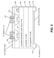
- FIG. 5 illustrates an embodiment of a planar PIN photodetector using lattice-matched In x Ga 1-x As 1-y-z Sb y N z as the photoabsorber material in accordance with one or more embodiments of the present invention
- FIG. 6 illustrates another embodiment where the In x Ga 1-x As 1-y-z Sb y N z is used in a mesa PIN photodetector
- FIG. 7 illustrates another embodiment where the In x Ga 1-x As 1-y-z Sb y N z is used in an Avalanche Photodetector.
- FIG. 3 A preferred embodiment of the invention is shown in FIG. 3 .
- An n-type InP buffer layer 6 that is 1 micron is grown on an n-type InP substrate 5 .
- a 3.5 micron thick layer of InGaAsSbN 7 is grown on top of the buffer layer 6 .
- Layer 7 is grown with light n-doping.
- a 1 micron thick InP layer 8 is grown on top of the photoabsorbing layer 7 .
- a 0.2 micron layer of InGaAs 9 is grown on top of InP layer 8 to provide a low-resistance Ohmic contact.
- the In x Ga 1-x As 1-y-z Sb y N z can be grown with a cutoff wavelength beyond 3 micron and still remain lattice-matched to the substrate 5 .
- the material can be grown in a number of ways, and is typically grown through epitaxial growth, such as metal-organic chemical vapor deposition or molecular beam epitaxy, but other methods can be used within the scope of the present invention.
- One embodiment to achieve lattice-matching is to iteratively approach the material beginning with In0.53Ga0.47As, which is lattice-matched to InP.
- the Indium and Gallium source flows are kept the same as the previous run, and N and Sb are introduced at a ratio of 1:2.6. This ratio is derived from Vegaard's law.
- 2% Sb would be used, which gives an N composition of 5.2%.
- the layer is annealed at 650-750° C. for 1-10 minutes to remove defects. The layer is analyzed by photoluminescence and x-ray diffraction. X-ray diffraction illustrates the lattice-mismatch.
- Lattice matching is often defined as a difference in layer x-ray peak and substrate x-ray peak by less than 400 arcsec.
- the photoluminescence peak wavelength will likely be approximately 2 microns.
- the Indium is increased. If the Indium is increased without changes to the As, Sb, or N flows, the mismatch between the lattice constant of the layer and the substrate will be large.
- the Nitrogen composition also increases; however, the As composition, and Sb composition will stay the same. While the increase in N composition will extend the wavelength, it offsets the strain caused by increased Indium flow.
- the Indium composition needs to increase to 75% (from 53%), and the N needs to increase to 8% (from approximately 2%), or In 0.75 Ga 0.25 As 0.82 Sb 0.05 N 0.08 .
- These numbers are approximate, and again, photoluminescence and x-ray diffraction can be used to iteratively achieve the wavelength and lattice-matching desired.
- the layer can be grown in the device structure shown in FIG. 3 . If the photoluminescence measures a wavelength of 2.5 micron of the given layer, the range of photon wavelengths to which the detector will be sensitive is from 0.92 microns to 2.5 microns.
- FIG. 4 reproduced from M. Gokhale, J. Wei, H. Wang, S. Forrest, “Growth and characterization of small band gap ( ⁇ 0.6 eV) InGaAsN layers on InP,” Applied Physics Letters, Vol. 74, pp. 1287-9 (1999), shows the approximate theoretical relationship between the N content and the bandgap of the InGaAsN. Not shown is the Sb incorporated in the preferred embodiment of this invention.
- the InGaAsSbN photoabsorbing layer is lattice-matched to the InP substrate, there is no need for a buffer layer that reduces the number of defects. Therefore the short end of the wavelength range is only limited by InP to be 920 nm, and not a longer wavelength.
- the wavelength range can be further extended into the visible by removing the substrate through a combination of mechanical lapping and wet etching.
- the layer 6 can be replaced by AlInAs which has a bandgap slightly lower than InP so that following substrate removal, the onset of optical absorption will be about 0.86 microns.
- FIG. 5 illustrates an embodiment of a planar PIN photodetector using lattice-matched In x Ga 1-x As 1-y-z SB y N z as the photoabsorber material in accordance with one or more embodiments of the present invention.
- the structure shown in FIG. 5 is grown on an n-type InP substrate 500 .
- the structure can also be grown on a semi-insulating InP substrate 500 .
- the first layer is the n-type InP window layer 502 which provides a barrier to photocarriers generated within the absorbing area.
- the next layer is the photoabsorbing layer 504 , and it is composed of In x Ga 1-x As 1-y-z Sb y N z .
- the photoabsorbing layer 504 can be undoped or lightly n-doped at approximately 5E15 cm-3. In the preferred embodiment, this layer is 3.5 ums thick, but it can range from 0.1-10 ums, depending on the application.
- a lightly n-doped InP layer 506 is grown. This layer is typically 1 micron thick, but can be of any thickness without departing from the scope of the present invention.
- the top layer is the InGaAs contact layer 508 , which is typically 0.2 microns thick, but can be of any thickness or not present, without departing from the scope of the present invention.
- the top layer 508 is also typically undoped.
- the InGaAs contact layer 508 is etched into a mesa, and then Zn is typically diffused into the cap structure in areas 510 to make it p-type and define the PIN junction. The Zn diffuses through the InP layer 506 until it reaches the photoabsorbing layer 504 .
- the p-side 512 and n-side 514 contacts are provided to fully form the detector.
- An anti-reflection coating can also be applied to the bottom of substrate 500 if desired.
- FIG. 6 illustrates another embodiment where the In x Ga 1-x As 1-y-z Sb y N z is used in a mesa PIN photodetector.
- the structure is grown on a n-type or semi-insulating InP substrate 500 .
- a first InP layer 502 is grown to be 1 micron and n-type.
- the photoabsorbing layer 504 In x Ga 1-x As 1-y-z Sb y N z , is grown to be 3.5 microns and lightly n-type.
- a second InP layer 506 is grown to be 1 micron and p-type.
- an InGaAs contact layer 508 is grown to be 0.2 microns and heavily p-type.
- the device is defined photolithographically into a circle or square, and the outer edge is etched away.
- a passivation layer 600 is deposited on the edges to minimize leakage current.
- Metallic contacts 512 and 514 are deposited on the p-layer 508 and n-layer 502 .
- FIG. 7 illustrates another embodiment where the In x Ga 1-x As 1-y-z Sb y N z is used in an Avalanche Photodetector.
- the layer structure comprises an InP substrate 500 that is comprised of one of an n-type dopants or semi-insulating dopants; an n-doped InP buffer layer 502 ; an n-doped AlInAs field stop layer 700 ; an undoped AlInAs multiplication layer 702 ; a p-doped AlInAs field charge layer 704 ; an undoped photoabsorbing layer 504 made using In x Ga 1-x As 1-y-z Sb y N z ; a p-doped InP contact layer 506 ; and a p-doped InGaAs contact layer 508 .
- Diodes are formed by etching mesas and passivating the sidewalls.
- Metallic contacts 512 and 514 are made on both the p-InGaAs contact layer and on the n-doped InP buffer. This structure will provide high-gain, low noise photodetector performance and be sensitive to wavelengths beyond 3 microns. This structure is challenging to make with In 0.75 Ga 0.25 As photoabsorbing layer 508 because said layer has a high number of defects which lead to high dark current.
- Other Avalanche Photodetector designs can be implemented with the scope of the present invention.
- the single detector can also be made into an array of detectors.
- these detector arrays would typically be bump-bonded to a readout integrated circuit.
- the present invention describes embodiments of detectors made using photoabsorbing layers lattice matched to InP for achieving cutoff wavelengths beyond 1.7 microns.
- a photodiode apparatus in accordance with one or more embodiments of the present invention comprises an indium phosphide substrate, and a photoabsorbing region comprising at least an indium gallium arsenide antimonide nitride (InGaAsSbN) layer, wherein the InGaAsSbN layer has a thickness of at least 100 nanometers and is nominally lattice-matched to the indium phosphide substrate.
- InGaAsSbN indium gallium arsenide antimonide nitride
- Such a photodiode apparatus further optionally comprises the photoabsorbing region having a cutoff wavelength greater than 1.7 microns, the cutoff wavelength being measured at 25 degrees celsius, the cutoff wavelength being less than 5 microns, the thickness of the InGaAsSbN layer being between 0.05 microns and 10 microns, the InGaAsSbN layer comprising a concentration of 0.5% to 15% of antimonide, the InGaAsSbN layer comprising a concentration of 0.5% to 15% of nitrogen, the InGaAsSbN layer comprising a concentration greater than 40% of indium, and the indium phosphide substrate being substantially removed.
- Another photodiode apparatus in accordance with one or more embodiments of the present invention comprises an indium phosphide substrate, a first layer region coupled to the indium phosphide, the first layer comprising at least a layer of indium phosphide doped n-type material, a second layer region, coupled to the first layer region, the second layer region comprising at least an indium gallium arsenide antimonide nitride (InGaAsSbN) layer, the InGaAsSbN layer having a thickness of at least 100 nanometers and being nominally lattice-matched to said substrate, a third layer region comprising a layer of indium phosphide, a fourth layer region comprising a patterned p-type layer of indium gallium arsenide, and a fifth layer region comprising a dopant diffused region which extends from said third layer region into said second layer region.
- InGaAsSbN indium gallium arsenide antimonide
Abstract
Description
Claims (9)
Priority Applications (2)
| Application Number | Priority Date | Filing Date | Title |
|---|---|---|---|
| US12/254,634 US7915639B2 (en) | 2008-10-20 | 2008-10-20 | InGaAsSbN photodiode arrays |
| US13/070,829 US8324659B2 (en) | 2008-10-20 | 2011-03-24 | InGaAsSbN photodiode arrays |
Applications Claiming Priority (1)
| Application Number | Priority Date | Filing Date | Title |
|---|---|---|---|
| US12/254,634 US7915639B2 (en) | 2008-10-20 | 2008-10-20 | InGaAsSbN photodiode arrays |
Related Child Applications (1)
| Application Number | Title | Priority Date | Filing Date |
|---|---|---|---|
| US13/070,829 Continuation US8324659B2 (en) | 2008-10-20 | 2011-03-24 | InGaAsSbN photodiode arrays |
Publications (2)
| Publication Number | Publication Date |
|---|---|
| US20100096665A1 US20100096665A1 (en) | 2010-04-22 |
| US7915639B2 true US7915639B2 (en) | 2011-03-29 |
Family
ID=42107954
Family Applications (2)
| Application Number | Title | Priority Date | Filing Date |
|---|---|---|---|
| US12/254,634 Active 2029-01-15 US7915639B2 (en) | 2008-10-20 | 2008-10-20 | InGaAsSbN photodiode arrays |
| US13/070,829 Active US8324659B2 (en) | 2008-10-20 | 2011-03-24 | InGaAsSbN photodiode arrays |
Family Applications After (1)
| Application Number | Title | Priority Date | Filing Date |
|---|---|---|---|
| US13/070,829 Active US8324659B2 (en) | 2008-10-20 | 2011-03-24 | InGaAsSbN photodiode arrays |
Country Status (1)
| Country | Link |
|---|---|
| US (2) | US7915639B2 (en) |
Families Citing this family (10)
| Publication number | Priority date | Publication date | Assignee | Title |
|---|---|---|---|---|
| US8963274B2 (en) * | 2013-03-15 | 2015-02-24 | Sensors Unlimited, Inc. | Epitaxial structure for vertically integrated charge transfer gate technology in optoelectronic materials |
| EP3103142B1 (en) | 2014-02-05 | 2020-08-19 | Array Photonics, Inc. | Monolithic multijunction power converter |
| JP2018518848A (en) * | 2015-06-22 | 2018-07-12 | アイキューイー ピーエルシーIQE plc | Photoelectron detector with a dilute nitride layer on a substrate with a lattice parameter that closely matches GaAs. |
| TWI718159B (en) * | 2015-06-22 | 2021-02-11 | 英商Iqe公司 | OPTOELECTRONIC DETECTORS HAVING A DILUTE NITRIDE LAYER ON A SUBSTRATE WITH A LATTICE PARAMETER NEARLY MATCHING GaAs |
| WO2019010037A1 (en) | 2017-07-06 | 2019-01-10 | Solar Junction Corporation | Hybrid mocvd/mbe epitaxial growth of high-efficiency lattice-matched multijunction solar cells |
| JP6943078B2 (en) * | 2017-08-23 | 2021-09-29 | 富士通株式会社 | Infrared detector and its manufacturing method, image sensor, image system |
| WO2019067553A1 (en) | 2017-09-27 | 2019-04-04 | Solar Junction Corporation | Short wavelength infrared optoelectronic devices having a dilute nitride layer |
| JP7344912B2 (en) * | 2018-07-11 | 2023-09-14 | エスアールアイ インターナショナル | Linear mode avalanche photodiode without excessive noise |
| WO2020185528A1 (en) | 2019-03-11 | 2020-09-17 | Array Photonics, Inc. | Short wavelength infrared optoelectronic devices having graded or stepped dilute nitride active regions |
| CN113363341A (en) * | 2021-06-24 | 2021-09-07 | 湖南汇思光电科技有限公司 | PIN type InGaAsSb detector and preparation method thereof |
Citations (2)
| Publication number | Priority date | Publication date | Assignee | Title |
|---|---|---|---|---|
| US4032951A (en) * | 1976-04-13 | 1977-06-28 | Bell Telephone Laboratories, Incorporated | Growth of iii-v layers containing arsenic, antimony and phosphorus, and device uses |
| JP2006278397A (en) * | 2005-03-28 | 2006-10-12 | Nippon Telegr & Teleph Corp <Ntt> | Pseudomorphic quantum well structure and manufacturing method thereof |
Family Cites Families (1)
| Publication number | Priority date | Publication date | Assignee | Title |
|---|---|---|---|---|
| JP3910817B2 (en) * | 2000-12-19 | 2007-04-25 | ユーディナデバイス株式会社 | Semiconductor photo detector |
-
2008
- 2008-10-20 US US12/254,634 patent/US7915639B2/en active Active
-
2011
- 2011-03-24 US US13/070,829 patent/US8324659B2/en active Active
Patent Citations (2)
| Publication number | Priority date | Publication date | Assignee | Title |
|---|---|---|---|---|
| US4032951A (en) * | 1976-04-13 | 1977-06-28 | Bell Telephone Laboratories, Incorporated | Growth of iii-v layers containing arsenic, antimony and phosphorus, and device uses |
| JP2006278397A (en) * | 2005-03-28 | 2006-10-12 | Nippon Telegr & Teleph Corp <Ntt> | Pseudomorphic quantum well structure and manufacturing method thereof |
Non-Patent Citations (1)
| Title |
|---|
| Fu et al., "Solid-source molecular-beam epitaxy growth of GaInNAsSb/InGaAs single quantum well on InP with photoluminescence peak wavelength at 2.04 um", Journal of Vacuum Science Technology B vol. 22, No. 3, May/Jun. 2004 pp. 1463-1467. * |
Also Published As
| Publication number | Publication date |
|---|---|
| US8324659B2 (en) | 2012-12-04 |
| US20100096665A1 (en) | 2010-04-22 |
| US20110169048A1 (en) | 2011-07-14 |
Similar Documents
| Publication | Publication Date | Title |
|---|---|---|
| US7915639B2 (en) | InGaAsSbN photodiode arrays | |
| US9178089B1 (en) | Strain-balanced extended-wavelength barrier detector | |
| US9391229B2 (en) | Light receiving element, semiconductor epitaxial wafer, detecting device, and method for manufacturing light receiving element | |
| US8058642B2 (en) | Light-receiving device | |
| Bank et al. | Avalanche photodiodes based on the AlInAsSb materials system | |
| Teng et al. | High-performance long-wavelength InAs/GaSb superlattice detectors grown by MOCVD | |
| TWI717756B (en) | Optoelectronic devices having a dilute nitride layer | |
| US20150179863A1 (en) | Avalanche photodiode utilizing interfacial misfit array | |
| Arslan et al. | \(640\times 512\) Extended Short Wavelength Infrared In 0.83 Ga 0.17 As Focal Plane Array | |
| US20230327040A1 (en) | Avalanche photo diode | |
| Mohammedy et al. | Growth and fabrication issues of GaSb-based detectors | |
| Gomółka et al. | Mid-wave InAs/GaSb superlattice barrier infrared detectors with nBnN and pBnN design | |
| Huang et al. | Short/mid-wave two-band type-II superlattice infrared heterojunction phototransistor | |
| Lubyshev et al. | MBE growth of Sb-based type-II strained layer superlattice structures on multiwafer production reactors | |
| US20150162471A1 (en) | Phototransistor device | |
| Field et al. | Electrical and optical performance of InAs/GaSb superlattice LWIR detectors | |
| Suo et al. | Dark Current Analysis of InAsSb-Based Hetero-$ p {\text {-}} i {\text {-}} n $ Mid-Infrared Photodiode | |
| JP5391945B2 (en) | Light receiving element and epitaxial wafer | |
| RU2627146C1 (en) | Mesastructural photodiode based on heteroepitaxial structure of ingaas / alinas / inp | |
| Korotcenkov | ZnSe-Based Photodetectors | |
| Maddox | High-gain, low-noise avalanche photodiodes grown by molecular beam epitaxy | |
| Wojtczuk et al. | High-quantum-efficiency 2.2-um InGaAs MOCVD photodiodes | |
| Zhu et al. | Low Dark Current HgCdTe Long Wavelength Infrared Photodiodes with Bandgap Gradient Multi-Layer Heterojunction | |
| Khoshakhlagh et al. | Long wavelength InAs/GaSb superlattice detectors based on nBn and pin design | |
| Kim et al. | Improved performance of InAs/GaSb strained layer superlattice detectors with SU-8 passivation |
Legal Events
| Date | Code | Title | Description |
|---|---|---|---|
| AS | Assignment |
Owner name: AERIUS PHOTONICS LLC,CALIFORNIA Free format text: ASSIGNMENT OF ASSIGNORS INTEREST;ASSIGNORS:MACDOUGAL, MICHAEL;GESKE, JONATHAN;BOWERS, JOHN E.;SIGNING DATES FROM 20090101 TO 20090102;REEL/FRAME:022056/0884 Owner name: AERIUS PHOTONICS LLC, CALIFORNIA Free format text: ASSIGNMENT OF ASSIGNORS INTEREST;ASSIGNORS:MACDOUGAL, MICHAEL;GESKE, JONATHAN;BOWERS, JOHN E.;SIGNING DATES FROM 20090101 TO 20090102;REEL/FRAME:022056/0884 |
|
| STCF | Information on status: patent grant |
Free format text: PATENTED CASE |
|
| AS | Assignment |
Owner name: FLIR COMMERCIAL SYSTEMS, INC., OREGON Free format text: ASSIGNMENT OF ASSIGNORS INTEREST;ASSIGNOR:AERIUS PHOTONICS, LLC;REEL/FRAME:027802/0045 Effective date: 20110721 |
|
| AS | Assignment |
Owner name: FLIR SYSTEMS, INC., OREGON Free format text: ASSIGNMENT OF ASSIGNORS INTEREST;ASSIGNOR:FLIR COMMERCIAL SYSTEMS, INC.;REEL/FRAME:029168/0505 Effective date: 20121018 |
|
| FEPP | Fee payment procedure |
Free format text: PAT HOLDER NO LONGER CLAIMS SMALL ENTITY STATUS, ENTITY STATUS SET TO UNDISCOUNTED (ORIGINAL EVENT CODE: STOL); ENTITY STATUS OF PATENT OWNER: LARGE ENTITY |
|
| FPAY | Fee payment |
Year of fee payment: 4 |
|
| MAFP | Maintenance fee payment |
Free format text: PAYMENT OF MAINTENANCE FEE, 8TH YEAR, LARGE ENTITY (ORIGINAL EVENT CODE: M1552); ENTITY STATUS OF PATENT OWNER: LARGE ENTITY Year of fee payment: 8 |
|
| AS | Assignment |
Owner name: TELEDYNE FLIR, LLC, CALIFORNIA Free format text: MERGER AND CHANGE OF NAME;ASSIGNORS:FLIR SYSTEMS, INC.;FIREWORK MERGER SUB II, LLC;REEL/FRAME:058832/0915 Effective date: 20210514 |
|
| MAFP | Maintenance fee payment |
Free format text: PAYMENT OF MAINTENANCE FEE, 12TH YEAR, LARGE ENTITY (ORIGINAL EVENT CODE: M1553); ENTITY STATUS OF PATENT OWNER: LARGE ENTITY Year of fee payment: 12 |