US8324659B2 - InGaAsSbN photodiode arrays - Google Patents

InGaAsSbN photodiode arrays Download PDF

Info

Publication number
US8324659B2
US8324659B2 US13/070,829 US201113070829A US8324659B2 US 8324659 B2 US8324659 B2 US 8324659B2 US 201113070829 A US201113070829 A US 201113070829A US 8324659 B2 US8324659 B2 US 8324659B2
Authority
US
United States
Prior art keywords
layer
ingaassbn
microns
indium
photodiode
Prior art date
Legal status (The legal status is an assumption and is not a legal conclusion. Google has not performed a legal analysis and makes no representation as to the accuracy of the status listed.)
Active
Application number
US13/070,829
Other versions
US20110169048A1 (en
Inventor
Michael MacDougal
Jonathan Geske
John E. Bowers
Current Assignee (The listed assignees may be inaccurate. Google has not performed a legal analysis and makes no representation or warranty as to the accuracy of the list.)
Teledyne Flir LLC
Original Assignee
Aerius Photonics LLC
Priority date (The priority date is an assumption and is not a legal conclusion. Google has not performed a legal analysis and makes no representation as to the accuracy of the date listed.)
Filing date
Publication date
Application filed by Aerius Photonics LLC filed Critical Aerius Photonics LLC
Priority to US13/070,829 priority Critical patent/US8324659B2/en
Publication of US20110169048A1 publication Critical patent/US20110169048A1/en
Assigned to AERIUS PHOTONICS LLC reassignment AERIUS PHOTONICS LLC ASSIGNMENT OF ASSIGNORS INTEREST (SEE DOCUMENT FOR DETAILS). Assignors: GESKE, JONATHAN, MACDOUGAL, MICHAEL, BOWERS, JOHN E.
Assigned to FLIR COMMERCIAL SYSTEMS, INC. reassignment FLIR COMMERCIAL SYSTEMS, INC. ASSIGNMENT OF ASSIGNORS INTEREST (SEE DOCUMENT FOR DETAILS). Assignors: AERIUS PHOTONICS, LLC
Assigned to FLIR SYSTEMS, INC. reassignment FLIR SYSTEMS, INC. ASSIGNMENT OF ASSIGNORS INTEREST (SEE DOCUMENT FOR DETAILS). Assignors: FLIR COMMERCIAL SYSTEMS, INC.
Application granted granted Critical
Publication of US8324659B2 publication Critical patent/US8324659B2/en
Assigned to TELEDYNE FLIR, LLC reassignment TELEDYNE FLIR, LLC MERGER AND CHANGE OF NAME (SEE DOCUMENT FOR DETAILS). Assignors: FIREWORK MERGER SUB II, LLC, FLIR SYSTEMS, INC.
Active legal-status Critical Current
Anticipated expiration legal-status Critical

Links

Images

Classifications

    • HELECTRICITY
    • H01ELECTRIC ELEMENTS
    • H01LSEMICONDUCTOR DEVICES NOT COVERED BY CLASS H10
    • H01L31/00Semiconductor devices sensitive to infrared radiation, light, electromagnetic radiation of shorter wavelength or corpuscular radiation and specially adapted either for the conversion of the energy of such radiation into electrical energy or for the control of electrical energy by such radiation; Processes or apparatus specially adapted for the manufacture or treatment thereof or of parts thereof; Details thereof
    • H01L31/08Semiconductor devices sensitive to infrared radiation, light, electromagnetic radiation of shorter wavelength or corpuscular radiation and specially adapted either for the conversion of the energy of such radiation into electrical energy or for the control of electrical energy by such radiation; Processes or apparatus specially adapted for the manufacture or treatment thereof or of parts thereof; Details thereof in which radiation controls flow of current through the device, e.g. photoresistors
    • H01L31/10Semiconductor devices sensitive to infrared radiation, light, electromagnetic radiation of shorter wavelength or corpuscular radiation and specially adapted either for the conversion of the energy of such radiation into electrical energy or for the control of electrical energy by such radiation; Processes or apparatus specially adapted for the manufacture or treatment thereof or of parts thereof; Details thereof in which radiation controls flow of current through the device, e.g. photoresistors characterised by potential barriers, e.g. phototransistors
    • H01L31/101Devices sensitive to infrared, visible or ultraviolet radiation
    • H01L31/102Devices sensitive to infrared, visible or ultraviolet radiation characterised by only one potential barrier
    • H01L31/105Devices sensitive to infrared, visible or ultraviolet radiation characterised by only one potential barrier the potential barrier being of the PIN type
    • HELECTRICITY
    • H01ELECTRIC ELEMENTS
    • H01LSEMICONDUCTOR DEVICES NOT COVERED BY CLASS H10
    • H01L31/00Semiconductor devices sensitive to infrared radiation, light, electromagnetic radiation of shorter wavelength or corpuscular radiation and specially adapted either for the conversion of the energy of such radiation into electrical energy or for the control of electrical energy by such radiation; Processes or apparatus specially adapted for the manufacture or treatment thereof or of parts thereof; Details thereof
    • H01L31/0248Semiconductor devices sensitive to infrared radiation, light, electromagnetic radiation of shorter wavelength or corpuscular radiation and specially adapted either for the conversion of the energy of such radiation into electrical energy or for the control of electrical energy by such radiation; Processes or apparatus specially adapted for the manufacture or treatment thereof or of parts thereof; Details thereof characterised by their semiconductor bodies
    • H01L31/0256Semiconductor devices sensitive to infrared radiation, light, electromagnetic radiation of shorter wavelength or corpuscular radiation and specially adapted either for the conversion of the energy of such radiation into electrical energy or for the control of electrical energy by such radiation; Processes or apparatus specially adapted for the manufacture or treatment thereof or of parts thereof; Details thereof characterised by their semiconductor bodies characterised by the material
    • H01L31/0264Inorganic materials
    • H01L31/0304Inorganic materials including, apart from doping materials or other impurities, only AIIIBV compounds
    • H01L31/03046Inorganic materials including, apart from doping materials or other impurities, only AIIIBV compounds including ternary or quaternary compounds, e.g. GaAlAs, InGaAs, InGaAsP
    • HELECTRICITY
    • H01ELECTRIC ELEMENTS
    • H01LSEMICONDUCTOR DEVICES NOT COVERED BY CLASS H10
    • H01L31/00Semiconductor devices sensitive to infrared radiation, light, electromagnetic radiation of shorter wavelength or corpuscular radiation and specially adapted either for the conversion of the energy of such radiation into electrical energy or for the control of electrical energy by such radiation; Processes or apparatus specially adapted for the manufacture or treatment thereof or of parts thereof; Details thereof
    • H01L31/08Semiconductor devices sensitive to infrared radiation, light, electromagnetic radiation of shorter wavelength or corpuscular radiation and specially adapted either for the conversion of the energy of such radiation into electrical energy or for the control of electrical energy by such radiation; Processes or apparatus specially adapted for the manufacture or treatment thereof or of parts thereof; Details thereof in which radiation controls flow of current through the device, e.g. photoresistors
    • H01L31/10Semiconductor devices sensitive to infrared radiation, light, electromagnetic radiation of shorter wavelength or corpuscular radiation and specially adapted either for the conversion of the energy of such radiation into electrical energy or for the control of electrical energy by such radiation; Processes or apparatus specially adapted for the manufacture or treatment thereof or of parts thereof; Details thereof in which radiation controls flow of current through the device, e.g. photoresistors characterised by potential barriers, e.g. phototransistors
    • H01L31/101Devices sensitive to infrared, visible or ultraviolet radiation
    • H01L31/102Devices sensitive to infrared, visible or ultraviolet radiation characterised by only one potential barrier
    • H01L31/107Devices sensitive to infrared, visible or ultraviolet radiation characterised by only one potential barrier the potential barrier working in avalanche mode, e.g. avalanche photodiodes
    • YGENERAL TAGGING OF NEW TECHNOLOGICAL DEVELOPMENTS; GENERAL TAGGING OF CROSS-SECTIONAL TECHNOLOGIES SPANNING OVER SEVERAL SECTIONS OF THE IPC; TECHNICAL SUBJECTS COVERED BY FORMER USPC CROSS-REFERENCE ART COLLECTIONS [XRACs] AND DIGESTS
    • Y02TECHNOLOGIES OR APPLICATIONS FOR MITIGATION OR ADAPTATION AGAINST CLIMATE CHANGE
    • Y02EREDUCTION OF GREENHOUSE GAS [GHG] EMISSIONS, RELATED TO ENERGY GENERATION, TRANSMISSION OR DISTRIBUTION
    • Y02E10/00Energy generation through renewable energy sources
    • Y02E10/50Photovoltaic [PV] energy
    • Y02E10/544Solar cells from Group III-V materials

Definitions

  • This invention relates generally to light detection and photodiode arrays, and in particular to arrays made from indium gallium arsenide and related materials.
  • FIG. 1 illustrates a description of this approach, where the substrate InP 1 has a buffer layer of InGaAs 2 followed by the absorption layer InGaAs 3 , followed by an InP cap 4 .
  • the InGaAs absorber 3 has a x-value that is greater than 0.53, and therefore is no longer lattice-matched with the InP substrate 1 .
  • FIG. 2 illustrates the relationship of the x-value in InGaAs with the lattice-matching to InP substrate and the emission wavelength.
  • the wavelength range is extended, but again, the material is no longer lattice-matched to the InP substrate 1 . Because the material is no longer lattice-matched, dislocation defects are created in the material, which increase the dark current by several orders of magnitude over what the material should achieve theoretically.
  • the InGaAs buffer layer 2 is used to reduce the number of defects, but they cannot be completely eliminated because they propagate through the grown layer into the absorber.
  • the InGaAs buffer layer 2 also limits the short wavelength range which is normally limited by InP to a wavelength of 920 nm.
  • the InGaAs buffer layer 2 can increase the short wavelength to 1100 nm or higher, which is undesirable because it decreases the overall wavelength range from the detector.
  • Thin layers of InGaAsSbN have been grown on InP to demonstrate extension of the laser emission wavelength [J. Fu, S. Bank, M. Wistey, H. Yuen, J. Harris, Jr., “Solid-source molecular-beam epitaxy growth of GaInNAsSb/InGaAs single quantum well on InP with photoluminescence peak wavelength at 2.04 microns,” Journal of Vacuum Science Technology B, vol. 22, no 3, pp. 1463-7], which is incorporated by reference herein.
  • the present invention discloses a semiconductor device comprised of several layers, wherein the photoabsorbing layer is a thick (>0.1 micron), lattice-matched layer that can be used for the detection of infrared light.
  • a photodiode apparatus in accordance with one or more embodiments of the present invention comprises an indium phosphide substrate, and a photoabsorbing region comprising at least an indium gallium arsenide antimonide nitride (InGaAsSbN) layer, wherein the InGaAsSbN layer has a thickness of at least 100 nanometers and is nominally lattice-matched to the indium phosphide substrate.
  • InGaAsSbN indium gallium arsenide antimonide nitride
  • Such a photodiode apparatus further optionally comprises the photoabsorbing region having a cutoff wavelength greater than 1.7 microns, the cutoff wavelength being measured at 25 degrees celsius, the cutoff wavelength being less than 3 microns, the thickness of the InGaAsSbN layer being between 0.05 microns and 7 microns, the InGaAsSbN layer comprising a concentration of 0.5% to 15% of antimonide, the InGaAsSbN layer comprising a concentration of 0.5% to 15% of nitrogen, the InGaAsSbN layer comprising a concentration greater than 40% of indium, and the indium phosphide substrate being substantially removed.
  • Another photodiode apparatus in accordance with one or more embodiments of the present invention comprises an indium phosphide substrate, a first layer region coupled to the indium phosphide, the first layer comprising at least a layer of indium phosphide doped n-type material, a second layer region, coupled to the first layer region, the second layer region comprising at least an indium gallium arsenide antimonide nitride (InGaAsSbN) layer, the InGaAsSbN layer having a thickness of at least 100 nanometers and being nominally lattice-matched to said substrate, a third layer region comprising a layer of indium phosphide, a fourth layer region comprising a patterned p-type layer of indium gallium arsenide, and a fifth layer region comprising a dopant diffused region which extends from said third layer region into said second layer region.
  • InGaAsSbN indium gallium arsenide antimonide
  • FIG. 1 illustrates a device having an increase in the Indium composition
  • FIG. 2 illustrates the relationship of the x-value in InGaAs with the lattice-matching to InP substrate and the emission wavelength
  • FIG. 3 illustrates a preferred embodiment of the present invention
  • FIG. 4 illustrates the approximate theoretical relationship between the N content and the bandgap of the InGaAsN material
  • FIG. 5 illustrates an embodiment of a planar PIN photodetector using lattice-matched In x Ga 1 ⁇ x As 1 ⁇ y ⁇ z Sb y N z as the photoabsorber material in accordance with one or more embodiments of the present invention
  • FIG. 6 illustrates another embodiment where the In x G 1 ⁇ x As 1 ⁇ y ⁇ z Sb y N z is used in a mesa PIN photodetector
  • FIG. 7 illustrates another embodiment where the In x Ga 1 ⁇ x As 1 ⁇ y ⁇ z Sb y N z is used in an Avalanche Photodetector.
  • FIG. 3 A preferred embodiment of the invention is shown in FIG. 3 .
  • An n-type InP buffer layer 6 that is 1 micron thick is grown on an n-type InP substrate 5 .
  • a 3.5 micron thick layer of InGaAsSbN 7 is grown on top of the buffer layer 6 .
  • Layer 7 is grown with light n-doping.
  • a 1 micron thick InP layer 8 is grown on top of the photoabsorbing layer 7 .
  • a 0.2 micron layer of InGaAs 9 is grown on top of InP layer 8 to provide a low-resistance Ohmic contact.
  • the In x Ga 1 ⁇ x As 1 ⁇ y ⁇ z Sb y N z can be grown with a cutoff wavelength beyond 3 micron and still remain lattice-matched to the substrate 5 .
  • the material can be grown in a number of ways, and is typically grown through epitaxial growth, such as metal-organic chemical vapor deposition or molecular beam epitaxy, but other methods can be used within the scope of the present invention.
  • One embodiment to achieve lattice-matching is to iteratively approach the material beginning with In0.53Ga0.47As, which is lattice-matched to InP.
  • the Indium and Gallium source flows are kept the same as the previous run, and N and Sb are introduced at a ratio of 1:2.6. This ratio is derived from Vegard's law. As a starting point, 2% Sb would be used, which gives an N composition of 5.2%.
  • the layer is annealed at 650-750° C. for 1-10 minutes to remove defects. The layer is analyzed by photoluminescence and x-ray diffraction. X-ray diffraction illustrates the lattice-mismatch.
  • Lattice matching is often defined as a difference in layer x-ray peak and substrate x-ray peak by less than 400 arc sec.
  • the photoluminescence peak wavelength will likely be approximately 2 microns.
  • the Indium is typically increased. If the Indium is increased without changes to the As, Sb, or N flows, the mismatch between the lattice constant of the layer and the substrate will be large. To compensate for the increase in Indium composition, the Nitrogen composition also increases; however, the As composition, and Sb composition will stay the same. While the increase in N composition will extend the wavelength, it offsets the strain caused by increased Indium flow.
  • the Indium composition needs to increase to 75% (from 53%), and the N needs to increase to 8% (from approximately 2%), or In 0.75 Ga 0.25 As 0.82 Sb 0.05 N 0.08 .
  • These numbers are approximate, and again, photoluminescence and x-ray diffraction can be used to iteratively achieve the wavelength and lattice-matching desired.
  • the layer can be grown in the device structure shown in FIG. 3 . If the photoluminescence measures a wavelength of 2.5 micron of the given layer, the range of photon wavelengths to which the detector will be sensitive is from 0.92 microns to 2.5 microns.
  • FIG. 4 reproduced from M. Gokhale, J. Wei, H. Wang, S. Forrest, “Growth and characterization of small band gap ( ⁇ 0.6 eV) InGaAsN layers on InP,” Applied Physics Letters, Vol. 74, pp. 1287-9 (1999), shows the approximate theoretical relationship between the N content and the bandgap of the InGaAsN. Not shown is the Sb incorporated in the preferred embodiment of this invention.
  • the InGaAsSbN photoabsorbing layer is lattice-matched to the InP substrate, there is no need for a buffer layer that reduces the number of defects. Therefore the short end of the wavelength range is only limited by InP to be 920 nm, and not a longer wavelength.
  • the wavelength range can be further extended into the visible by removing the substrate through a combination of mechanical lapping and wet etching.
  • the layer 6 can be replaced by AlInAs which has a bandgap slightly lower than InP so that following substrate removal, the onset of optical absorption will be about 0.83 microns.
  • FIG. 5 illustrates an embodiment of a planar PIN photodetector using lattice-matched In x Ga 1 ⁇ x As 1 ⁇ y ⁇ z Sb y N z as the photoabsorber material in accordance with one or more embodiments of the present invention.
  • the structure shown in FIG. 5 is grown on an n-type InP substrate 500 .
  • the structure can also be grown on a semi-insulating InP substrate 500 .
  • the first layer is the n-type InP window layer 502 which provides a barrier to photocarriers generated within the absorbing area.
  • the next layer is the photoabsorbing layer 504 , and it is composed of In x Ga 1 ⁇ x As 1 ⁇ y ⁇ z Sb y N z .
  • the photoabsorbing layer 504 can be undoped or lightly n-doped at approximately 5E15 cm ⁇ 3. In the preferred embodiment, this layer is 3.5 ums thick, but it can range from 0.1-7 ums, depending on the application.
  • a lightly n-doped InP layer 506 is grown. This layer is typically 1 micron thick, but can be of any thickness without departing from the scope of the present invention.
  • the top layer is the InGaAs contact layer 508 , which is typically 0.2 microns thick, but can be of any thickness without departing from the scope of the present invention.
  • the top layer 508 is also typically undoped.
  • the InGaAs contact layer 508 is etched into a mesa, and then Zn is typically diffused into the cap structure in areas 510 to make it p-type and define the PIN junction. The Zn diffuses through the InP layer 506 until it reaches the photoabsorbing layer 504 .
  • the p-side 512 and n-side 514 contacts are provided to fully form the detector.
  • FIG. 6 illustrates another embodiment where the In x Ga 1 ⁇ x As 1 ⁇ y ⁇ z Sb y N z is used in a mesa PIN photodetector.
  • the structure is grown on a n-type or semi-insulating InP substrate 500 .
  • a first InP layer 502 is grown to be 1 micron and n-type.
  • the photoabsorbing layer 504 In x Ga 1 ⁇ x As 1 ⁇ y ⁇ z Sb y N z , is grown to be 3.5 microns and lightly n-type.
  • a second InP layer 506 is grown to be 1 micron and p-type.
  • an InGaAs contact layer 508 is grown to be 0.2 microns and heavily p-type.
  • the device is defined photolithographically into a circle or square, and the outer edge is etched away.
  • a passivation layer 600 is deposited on the edges to minimize leakage current.
  • Metallic contacts 512 and 514 are deposited on the p-layer 508 and n-layer 502 .
  • FIG. 7 illustrates another embodiment where the In x Ga 1 ⁇ x As 1 ⁇ y ⁇ z Sb y N z is used in an Avalanche Photodetector.
  • the layer structure comprises an InP substrate 500 that is comprised of one of an n-type dopants or semi-insulating dopants; an n-doped InP buffer layer 502 ; an n-doped AlInAs field stop layer 700 ; an undoped AlInAs multiplication layer 702 ; a p-doped AlInAs field charge layer 704 ; an undoped photoabsorbing layer 504 made using In x Ga 1 ⁇ x As 1 ⁇ y ⁇ z Sb y N z ; a p-doped InP contact layer 506 ; and a p-doped InGaAs contact layer 508 .
  • Diodes are formed by etching mesas and passivating the sidewalls.
  • Metallic contacts 512 and 514 are made on both the p-InGaAs contact layer and on the n-doped InP buffer. This structure will provide high-gain, low noise photodetector performance and be sensitive to wavelengths beyond 2.5 microns. This structure is challenging to make with In 0.75 Ga 0.25 As photoabsorbing layer 508 because said layer has a high number of defects which lead to high dark current.
  • Other Avalanche Photodetector designs can be implemented with the scope of the present invention.
  • the single detector can also be made into an array of detectors.
  • these detector arrays would typically be bump-bonded to a readout integrated circuit.
  • the present invention describes embodiments of detectors made using lattice matched photoabsorbing layers.
  • a photodiode apparatus in accordance with one or more embodiments of the present invention comprises an indium phosphide substrate, and a photoabsorbing region comprising at least an indium gallium arsenide antimonide nitride (InGaAsSbN) layer, wherein the InGaAsSbN layer has a thickness of at least 100 nanometers and is nominally lattice-matched to the indium phosphide substrate.
  • InGaAsSbN indium gallium arsenide antimonide nitride
  • Such a photodiode apparatus further optionally comprises the photoabsorbing region having a cutoff wavelength greater than 1.7 microns, the cutoff wavelength being measured at 25 degrees celsius, the cutoff wavelength being less than 3 microns, the thickness of the InGaAsSbN layer being between 0.05 microns and 7 microns, the InGaAsSbN layer comprising a concentration of 0.5% to 15% of antimonide, the InGaAsSbN layer comprising a concentration of 0.5% to 15% of nitrogen, the InGaAsSbN layer comprising a concentration greater than 40% of indium, and the indium phosphide substrate being substantially removed.
  • Another photodiode apparatus in accordance with one or more embodiments of the present invention comprises an indium phosphide substrate, a first layer region coupled to the indium phosphide, the first layer comprising at least a layer of indium phosphide doped n-type material, a second layer region, coupled to the first layer region, the second layer region comprising at least an indium gallium arsenide antimonide nitride (InGaAsSbN) layer, the InGaAsSbN layer having a thickness of at least 100 nanometers and being nominally lattice-matched to said substrate, a third layer region comprising a layer of indium phosphide, a fourth layer region comprising a patterned p-type layer of indium gallium arsenide, and a fifth layer region comprising a dopant diffused region which extends from said third layer region into said second layer region.
  • InGaAsSbN indium gallium arsenide antimonide

Landscapes

  • Physics & Mathematics (AREA)
  • Condensed Matter Physics & Semiconductors (AREA)
  • Electromagnetism (AREA)
  • General Physics & Mathematics (AREA)
  • Engineering & Computer Science (AREA)
  • Computer Hardware Design (AREA)
  • Microelectronics & Electronic Packaging (AREA)
  • Power Engineering (AREA)
  • Chemical & Material Sciences (AREA)
  • Inorganic Chemistry (AREA)
  • Light Receiving Elements (AREA)

Abstract

Embodiments of detectors made using lattice matched photoabsorbing layers are disclosed. A photodiode apparatus in accordance with one or more embodiments of the present invention comprises an indium phosphide substrate, and a photoabsorbing region comprising at least an indium gallium arsenide antimonide nitride (InGaAsSbN) layer, wherein the InGaAsSbN layer has a thickness of at least 100 nanometers and is nominally lattice-matched to the indium phosphide substrate.

Description

CROSS-REFERENCE TO RELATED APPLICATIONS
This application is a continuation of U.S. patent application Ser. No. 12/254,634, filed Oct. 20, 2008, entitled “InGaAsSbN PHOTODIODE ARRAYS,” which application is incorporated by reference herein.
BACKGROUND OF THE INVENTION
1. Field of the Invention
This invention relates generally to light detection and photodiode arrays, and in particular to arrays made from indium gallium arsenide and related materials.
2. Description of the Related Art
To extend the wavelength range of InxGa1−xAs detectors, the normal approach is to increase the Indium composition, or the x value [K. Ling a, G. Olsen, V. Ban, A. Joshi, W. Kosonocky, “Dark current analysis and characterization of InxGa1−xAs/InAsyP1−y graded photodiodes with x>0.53 for response to longer wavelengths (>1.7 microns), Journal of Lightwave Technology, vol. 10, pp. 1050-2 (1992)], which is incorporated by reference herein.
FIG. 1 illustrates a description of this approach, where the substrate InP 1 has a buffer layer of InGaAs 2 followed by the absorption layer InGaAs 3, followed by an InP cap 4. The InGaAs absorber 3 has a x-value that is greater than 0.53, and therefore is no longer lattice-matched with the InP substrate 1.
FIG. 2 illustrates the relationship of the x-value in InGaAs with the lattice-matching to InP substrate and the emission wavelength. By increasing the x-value from 0.53, the wavelength range is extended, but again, the material is no longer lattice-matched to the InP substrate 1. Because the material is no longer lattice-matched, dislocation defects are created in the material, which increase the dark current by several orders of magnitude over what the material should achieve theoretically. The InGaAs buffer layer 2 is used to reduce the number of defects, but they cannot be completely eliminated because they propagate through the grown layer into the absorber. The InGaAs buffer layer 2 also limits the short wavelength range which is normally limited by InP to a wavelength of 920 nm. The InGaAs buffer layer 2 can increase the short wavelength to 1100 nm or higher, which is undesirable because it decreases the overall wavelength range from the detector.
Other approaches have been made to extend the wavelength range in materials grown on InP substrates and GaAs substrates. One approach is to add Nitrogen to the InGaAs [D. Serries, T. Geppert, P. Ganser, M. Maier, K. Kohler, N. Herres, and J. Wagner, “Quaternary GaInAsN with high In content: Dependence of band gap energy on N content,” Applied Physics Letters, vol 80, no 14, pp. 2448-50], which is incorporated by reference herein. By growing thin layers of InGaAsN on InP, it has been demonstrated that the bandgap can be decreased to 590 meV, equivalent to a wavelength emission of 2.1 microns. However, the material exhibits poor photoluminescence which is indicative of a high concentration of defects.
Another approach introduces antimony (Sb) along with N to form InGaAsSbN to improve the photoluminescence[X. Yang, M. Jurkovic, J. Heroux, and W. Wang, “Molecular beam epitaxial growth InGaAsN:Sb/GaAs quantum wells for long-wavelength semiconductor lasers”, Applied Physics Letters, vol 75, no 2, pp. 178-80], which is incorporated by reference herein. The Sb is thought to act as a surfactant for the N and creates growth conditions that are more favorable for low defect growth, and devices made with such methods demonstrate laser emission wavelengths beyond 1 micron.
Thin layers of InGaAsSbN have been grown on InP to demonstrate extension of the laser emission wavelength [J. Fu, S. Bank, M. Wistey, H. Yuen, J. Harris, Jr., “Solid-source molecular-beam epitaxy growth of GaInNAsSb/InGaAs single quantum well on InP with photoluminescence peak wavelength at 2.04 microns,” Journal of Vacuum Science Technology B, vol. 22, no 3, pp. 1463-7], which is incorporated by reference herein. By using both N and Sb added to InGaAs, an extension of the wavelength from 1.7 microns to 2.04 microns was achieved, however, previous attempts to grow this material resulted in layers that are thin and strained, and therefore would not be useful for thick layer devices such as photodetectors.
It can be seen, then, that there is a need in the art for a lattice-matched material that has an extended wavelength response. It can also be seen that there is a need in the art for growing thick-layer compositions on InP to produce devices. It can also be seen that there is a need in the art to reduce dislocation defects in such devices to decrease the dark current.
SUMMARY OF THE INVENTION
To minimize the limitations in the prior art, and to minimize other limitations that will become apparent upon reading and understanding the present specification, the present invention discloses a semiconductor device comprised of several layers, wherein the photoabsorbing layer is a thick (>0.1 micron), lattice-matched layer that can be used for the detection of infrared light.
A photodiode apparatus in accordance with one or more embodiments of the present invention comprises an indium phosphide substrate, and a photoabsorbing region comprising at least an indium gallium arsenide antimonide nitride (InGaAsSbN) layer, wherein the InGaAsSbN layer has a thickness of at least 100 nanometers and is nominally lattice-matched to the indium phosphide substrate.
Such a photodiode apparatus further optionally comprises the photoabsorbing region having a cutoff wavelength greater than 1.7 microns, the cutoff wavelength being measured at 25 degrees celsius, the cutoff wavelength being less than 3 microns, the thickness of the InGaAsSbN layer being between 0.05 microns and 7 microns, the InGaAsSbN layer comprising a concentration of 0.5% to 15% of antimonide, the InGaAsSbN layer comprising a concentration of 0.5% to 15% of nitrogen, the InGaAsSbN layer comprising a concentration greater than 40% of indium, and the indium phosphide substrate being substantially removed.
Another photodiode apparatus in accordance with one or more embodiments of the present invention comprises an indium phosphide substrate, a first layer region coupled to the indium phosphide, the first layer comprising at least a layer of indium phosphide doped n-type material, a second layer region, coupled to the first layer region, the second layer region comprising at least an indium gallium arsenide antimonide nitride (InGaAsSbN) layer, the InGaAsSbN layer having a thickness of at least 100 nanometers and being nominally lattice-matched to said substrate, a third layer region comprising a layer of indium phosphide, a fourth layer region comprising a patterned p-type layer of indium gallium arsenide, and a fifth layer region comprising a dopant diffused region which extends from said third layer region into said second layer region.
BRIEF DESCRIPTION OF THE DRAWINGS
Referring now to the drawings in which like reference numbers represent corresponding parts throughout:
FIG. 1 illustrates a device having an increase in the Indium composition;
FIG. 2 illustrates the relationship of the x-value in InGaAs with the lattice-matching to InP substrate and the emission wavelength;
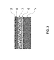
FIG. 3 illustrates a preferred embodiment of the present invention;
FIG. 4 illustrates the approximate theoretical relationship between the N content and the bandgap of the InGaAsN material;
FIG. 5 illustrates an embodiment of a planar PIN photodetector using lattice-matched InxGa1−xAs1−y−zSbyNz as the photoabsorber material in accordance with one or more embodiments of the present invention;
FIG. 6 illustrates another embodiment where the InxG1−xAs1−y−zSbyNz is used in a mesa PIN photodetector; and
FIG. 7 illustrates another embodiment where the InxGa1−xAs1−y−zSbyNz is used in an Avalanche Photodetector.
DETAILED DESCRIPTION OF THE PREFERRED EMBODIMENTS
In the following description, reference is made to the accompanying drawings which form a part hereof, and which is shown, by way of illustration, several embodiments of the present invention. It is understood that other embodiments may be utilized and structural changes may be made without departing from the scope of the present invention.
A preferred embodiment of the invention is shown in FIG. 3. An n-type InP buffer layer 6 that is 1 micron thick is grown on an n-type InP substrate 5. A 3.5 micron thick layer of InGaAsSbN 7 is grown on top of the buffer layer 6. Layer 7 is grown with light n-doping. A 1 micron thick InP layer 8 is grown on top of the photoabsorbing layer 7. Depending on the application, a 0.2 micron layer of InGaAs 9 is grown on top of InP layer 8 to provide a low-resistance Ohmic contact.
By using a preferred combination of constituent atoms, the InxGa1−xAs1−y−zSbyNz can be grown with a cutoff wavelength beyond 3 micron and still remain lattice-matched to the substrate 5. The material can be grown in a number of ways, and is typically grown through epitaxial growth, such as metal-organic chemical vapor deposition or molecular beam epitaxy, but other methods can be used within the scope of the present invention.
One embodiment to achieve lattice-matching is to iteratively approach the material beginning with In0.53Ga0.47As, which is lattice-matched to InP. In the next run, the Indium and Gallium source flows are kept the same as the previous run, and N and Sb are introduced at a ratio of 1:2.6. This ratio is derived from Vegard's law. As a starting point, 2% Sb would be used, which gives an N composition of 5.2%. After the growth, the layer is annealed at 650-750° C. for 1-10 minutes to remove defects. The layer is analyzed by photoluminescence and x-ray diffraction. X-ray diffraction illustrates the lattice-mismatch. If the lattice mismatch is tensile then Sb flow would be increased, and if the lattice mismatch is compressive, then N flow would be increased. The change in flow would be proportional to the difference in lattice mismatch. Another growth with new flows would be performed and characterized. This process would continue until lattice matching is achieved. Lattice matching is often defined as a difference in layer x-ray peak and substrate x-ray peak by less than 400 arc sec.
Once lattice matching has been achieved, the photoluminescence peak wavelength will likely be approximately 2 microns. For further increase in the emission wavelength, the Indium is typically increased. If the Indium is increased without changes to the As, Sb, or N flows, the mismatch between the lattice constant of the layer and the substrate will be large. To compensate for the increase in Indium composition, the Nitrogen composition also increases; however, the As composition, and Sb composition will stay the same. While the increase in N composition will extend the wavelength, it offsets the strain caused by increased Indium flow. To achieve a wavelength of 2.5 microns, the Indium composition needs to increase to 75% (from 53%), and the N needs to increase to 8% (from approximately 2%), or In0.75Ga0.25As0.82Sb0.05N0.08. These numbers are approximate, and again, photoluminescence and x-ray diffraction can be used to iteratively achieve the wavelength and lattice-matching desired. Once the desired wavelength has been achieved, the layer can be grown in the device structure shown in FIG. 3. If the photoluminescence measures a wavelength of 2.5 micron of the given layer, the range of photon wavelengths to which the detector will be sensitive is from 0.92 microns to 2.5 microns.
FIG. 4, reproduced from M. Gokhale, J. Wei, H. Wang, S. Forrest, “Growth and characterization of small band gap (˜0.6 eV) InGaAsN layers on InP,” Applied Physics Letters, Vol. 74, pp. 1287-9 (1999), shows the approximate theoretical relationship between the N content and the bandgap of the InGaAsN. Not shown is the Sb incorporated in the preferred embodiment of this invention.
Because the InGaAsSbN photoabsorbing layer is lattice-matched to the InP substrate, there is no need for a buffer layer that reduces the number of defects. Therefore the short end of the wavelength range is only limited by InP to be 920 nm, and not a longer wavelength. The wavelength range can be further extended into the visible by removing the substrate through a combination of mechanical lapping and wet etching. Alternatively, the layer 6 can be replaced by AlInAs which has a bandgap slightly lower than InP so that following substrate removal, the onset of optical absorption will be about 0.83 microns.
Detector Structures
FIG. 5 illustrates an embodiment of a planar PIN photodetector using lattice-matched InxGa1−xAs1−y−zSbyNz as the photoabsorber material in accordance with one or more embodiments of the present invention.
The structure shown in FIG. 5 is grown on an n-type InP substrate 500. In other embodiments where high switching speed is required, the structure can also be grown on a semi-insulating InP substrate 500. The first layer is the n-type InP window layer 502 which provides a barrier to photocarriers generated within the absorbing area. The next layer is the photoabsorbing layer 504, and it is composed of InxGa1−xAs1−y−zSbyNz. The photoabsorbing layer 504 can be undoped or lightly n-doped at approximately 5E15 cm−3. In the preferred embodiment, this layer is 3.5 ums thick, but it can range from 0.1-7 ums, depending on the application. Above the photoabsorbing layer 504, a lightly n-doped InP layer 506 is grown. This layer is typically 1 micron thick, but can be of any thickness without departing from the scope of the present invention. The top layer is the InGaAs contact layer 508, which is typically 0.2 microns thick, but can be of any thickness without departing from the scope of the present invention. The top layer 508 is also typically undoped. In the planar structure, the InGaAs contact layer 508 is etched into a mesa, and then Zn is typically diffused into the cap structure in areas 510 to make it p-type and define the PIN junction. The Zn diffuses through the InP layer 506 until it reaches the photoabsorbing layer 504. The p-side 512 and n-side 514 contacts are provided to fully form the detector.
FIG. 6 illustrates another embodiment where the InxGa1−xAs1−y−zSbyNz is used in a mesa PIN photodetector. In this embodiment, the structure is grown on a n-type or semi-insulating InP substrate 500. A first InP layer 502 is grown to be 1 micron and n-type. The photoabsorbing layer 504, InxGa1−xAs1−y−zSbyNz, is grown to be 3.5 microns and lightly n-type. A second InP layer 506 is grown to be 1 micron and p-type. Finally, an InGaAs contact layer 508 is grown to be 0.2 microns and heavily p-type. The device is defined photolithographically into a circle or square, and the outer edge is etched away. A passivation layer 600 is deposited on the edges to minimize leakage current. Metallic contacts 512 and 514 are deposited on the p-layer 508 and n-layer 502.
FIG. 7 illustrates another embodiment where the InxGa1−xAs1−y−zSbyNz is used in an Avalanche Photodetector. The layer structure comprises an InP substrate 500 that is comprised of one of an n-type dopants or semi-insulating dopants; an n-doped InP buffer layer 502; an n-doped AlInAs field stop layer 700; an undoped AlInAs multiplication layer 702; a p-doped AlInAs field charge layer 704; an undoped photoabsorbing layer 504 made using InxGa1−xAs1−y−zSbyNz; a p-doped InP contact layer 506; and a p-doped InGaAs contact layer 508. Diodes are formed by etching mesas and passivating the sidewalls. Metallic contacts 512 and 514 are made on both the p-InGaAs contact layer and on the n-doped InP buffer. This structure will provide high-gain, low noise photodetector performance and be sensitive to wavelengths beyond 2.5 microns. This structure is challenging to make with In0.75Ga0.25As photoabsorbing layer 508 because said layer has a high number of defects which lead to high dark current. Other Avalanche Photodetector designs can be implemented with the scope of the present invention.
In all of these embodiments, the single detector can also be made into an array of detectors. For imaging applications, these detector arrays would typically be bump-bonded to a readout integrated circuit.
Conclusion
In summary, the present invention describes embodiments of detectors made using lattice matched photoabsorbing layers.
A photodiode apparatus in accordance with one or more embodiments of the present invention comprises an indium phosphide substrate, and a photoabsorbing region comprising at least an indium gallium arsenide antimonide nitride (InGaAsSbN) layer, wherein the InGaAsSbN layer has a thickness of at least 100 nanometers and is nominally lattice-matched to the indium phosphide substrate.
Such a photodiode apparatus further optionally comprises the photoabsorbing region having a cutoff wavelength greater than 1.7 microns, the cutoff wavelength being measured at 25 degrees celsius, the cutoff wavelength being less than 3 microns, the thickness of the InGaAsSbN layer being between 0.05 microns and 7 microns, the InGaAsSbN layer comprising a concentration of 0.5% to 15% of antimonide, the InGaAsSbN layer comprising a concentration of 0.5% to 15% of nitrogen, the InGaAsSbN layer comprising a concentration greater than 40% of indium, and the indium phosphide substrate being substantially removed.
Another photodiode apparatus in accordance with one or more embodiments of the present invention comprises an indium phosphide substrate, a first layer region coupled to the indium phosphide, the first layer comprising at least a layer of indium phosphide doped n-type material, a second layer region, coupled to the first layer region, the second layer region comprising at least an indium gallium arsenide antimonide nitride (InGaAsSbN) layer, the InGaAsSbN layer having a thickness of at least 100 nanometers and being nominally lattice-matched to said substrate, a third layer region comprising a layer of indium phosphide, a fourth layer region comprising a patterned p-type layer of indium gallium arsenide, and a fifth layer region comprising a dopant diffused region which extends from said third layer region into said second layer region.
The foregoing description of the preferred embodiment of the invention has been presented for the purposes of illustration and description. It is not intended to be exhaustive or to limit the invention to the precise form disclosed. Many modifications and variations are possible in light of the above teaching. It is intended that the scope of the invention be limited not by this detailed description, but rather by the claims appended hereto and the full range of equivalents to the claims thereof.

Claims (18)

1. A photodiode apparatus, comprising:
an indium phosphide substrate; and
a photoabsorbing region comprising at least an indiumx gallium1−x arsenide antimonide nitride (InGaAsSbN) layer, wherein the InGaAsSbN layer has a thickness of at least 350 nanometers, the InGaAsSbN layer having a strain of within 0.3 percent of a lattice match between the indium phosphide substrate and the In GaAsSbN layer, and wherein x is greater than 0.53.
2. The photodiode apparatus of claim 1, wherein the photoabsorbing region has a cutoff wavelength greater than 1.7 microns.
3. The photodiode apparatus of claim 2, wherein the cutoff wavelength is measured at 25 degrees celsius.
4. The photodiode apparatus of claim 3, wherein the cutoff wavelength is less than 5 microns.
5. The photodiode apparatus of claim 1, wherein the thickness of the InGaAsSbN layer is between 0.05 microns and 10 microns.
6. The photodiode apparatus of claim 1, wherein the InGaAsSbN layer comprises a concentration of 0.5% to 15% of antimonide.
7. The photodiode apparatus of claim 1, wherein the InGaAsSbN layer comprises a concentration of 0.5% to 15% of nitrogen.
8. The photodiode apparatus of claim 1, wherein the InGaAsSbN layer comprises a concentration of 75% of indium.
9. The photodiode apparatus of claim 1, wherein the indium phosphide substrate is substantially removed.
10. A photodiode apparatus, comprising:
an indium phosphide substrate;
a first layer region coupled to the indium phosphide; and a second layer region, coupled to the first layer region, the second layer region comprising at least an indium gallium arsenide antimonide nitride (InxGa1−xAsSbN) layer, the InxGa1−xAsSbN layer having a thickness of at least 350 nanometers and having a strain of within 0.3 percent of a lattice match between the indium phosphide substrate and the InxGa1−xAsSbN layer, wherein the first layer region comprises at least a layer of material with a wider bandgap than the InxGa1−xAsSbN layer in the second layer region, and wherein x is greater than 0.53.
11. The photodiode apparatus of claim 10, wherein the second layer region has a cutoff wavelength greater than 1.7 microns.
12. The photodiode apparatus of claim 11, wherein the cutoff wavelength is measured at 25 degrees celsius.
13. The photodiode apparatus of claim 12, wherein the cutoff wavelength is less than 5 microns.
14. The photodiode apparatus of claim 10, wherein the thickness of the InGaAsSbN layer is between 0.05 microns and 10 microns.
15. The photodiode apparatus of claim 10, wherein the InGaAsSbN layer comprises a concentration of 0.5% to 15% of antimonide.
16. The photodiode apparatus of claim 10, wherein the InGaAsSbN layer comprises a concentration of 0.5% to 15% of nitrogen.
17. The photodiode apparatus of claim 10, wherein the InGaAsSbN layer comprises a concentration of 75% of indium.
18. The photodiode apparatus of claim 10, wherein the indium phosphide substrate is substantially removed.
US13/070,829 2008-10-20 2011-03-24 InGaAsSbN photodiode arrays Active US8324659B2 (en)

Priority Applications (1)

Application Number Priority Date Filing Date Title
US13/070,829 US8324659B2 (en) 2008-10-20 2011-03-24 InGaAsSbN photodiode arrays

Applications Claiming Priority (2)

Application Number Priority Date Filing Date Title
US12/254,634 US7915639B2 (en) 2008-10-20 2008-10-20 InGaAsSbN photodiode arrays
US13/070,829 US8324659B2 (en) 2008-10-20 2011-03-24 InGaAsSbN photodiode arrays

Related Parent Applications (1)

Application Number Title Priority Date Filing Date
US12/254,634 Continuation US7915639B2 (en) 2008-10-20 2008-10-20 InGaAsSbN photodiode arrays

Publications (2)

Publication Number Publication Date
US20110169048A1 US20110169048A1 (en) 2011-07-14
US8324659B2 true US8324659B2 (en) 2012-12-04

Family

ID=42107954

Family Applications (2)

Application Number Title Priority Date Filing Date
US12/254,634 Active 2029-01-15 US7915639B2 (en) 2008-10-20 2008-10-20 InGaAsSbN photodiode arrays
US13/070,829 Active US8324659B2 (en) 2008-10-20 2011-03-24 InGaAsSbN photodiode arrays

Family Applications Before (1)

Application Number Title Priority Date Filing Date
US12/254,634 Active 2029-01-15 US7915639B2 (en) 2008-10-20 2008-10-20 InGaAsSbN photodiode arrays

Country Status (1)

Country Link
US (2) US7915639B2 (en)

Cited By (1)

* Cited by examiner, † Cited by third party
Publication number Priority date Publication date Assignee Title
US8963274B2 (en) * 2013-03-15 2015-02-24 Sensors Unlimited, Inc. Epitaxial structure for vertically integrated charge transfer gate technology in optoelectronic materials

Families Citing this family (9)

* Cited by examiner, † Cited by third party
Publication number Priority date Publication date Assignee Title
US20150221803A1 (en) 2014-02-05 2015-08-06 Solar Junction Corporation Monolithic multijunction power converter
EP3311420A1 (en) * 2015-06-22 2018-04-25 IQE Plc. Optoelectronic detectors having a dilute nitride layer on a substrate with a lattice parameter nearly matching gaas
US9768339B2 (en) * 2015-06-22 2017-09-19 IQE, plc Optoelectronic detectors having a dilute nitride layer on a substrate with a lattice parameter nearly matching GaAs
WO2019010037A1 (en) 2017-07-06 2019-01-10 Solar Junction Corporation Hybrid mocvd/mbe epitaxial growth of high-efficiency lattice-matched multijunction solar cells
JP6943078B2 (en) * 2017-08-23 2021-09-29 富士通株式会社 Infrared detector and its manufacturing method, image sensor, image system
WO2019067553A1 (en) 2017-09-27 2019-04-04 Solar Junction Corporation Short wavelength infrared optoelectronic devices having a dilute nitride layer
EP3821472A4 (en) * 2018-07-11 2022-03-02 SRI International Linear mode avalanche photodiodes without excess noise
EP3939085A1 (en) 2019-03-11 2022-01-19 Array Photonics, Inc. Short wavelength infrared optoelectronic devices having graded or stepped dilute nitride active regions
CN113363341A (en) * 2021-06-24 2021-09-07 湖南汇思光电科技有限公司 PIN type InGaAsSb detector and preparation method thereof

Citations (1)

* Cited by examiner, † Cited by third party
Publication number Priority date Publication date Assignee Title
US7091527B2 (en) * 2000-12-19 2006-08-15 Fujitsu Quantum Devices Limited Semiconductor photodetection device

Family Cites Families (2)

* Cited by examiner, † Cited by third party
Publication number Priority date Publication date Assignee Title
US4032951A (en) * 1976-04-13 1977-06-28 Bell Telephone Laboratories, Incorporated Growth of iii-v layers containing arsenic, antimony and phosphorus, and device uses
JP4662345B2 (en) * 2005-03-28 2011-03-30 日本電信電話株式会社 Multiple strain quantum well structure and manufacturing method thereof

Patent Citations (1)

* Cited by examiner, † Cited by third party
Publication number Priority date Publication date Assignee Title
US7091527B2 (en) * 2000-12-19 2006-08-15 Fujitsu Quantum Devices Limited Semiconductor photodetection device

Non-Patent Citations (1)

* Cited by examiner, † Cited by third party
Title
Nakagawa et al., "Electroluminescence of InGaAsSbN quantum well diodes grown on InP substrates", 2004 International Conference on Indium Phosphide and Related Materials Conference Proceedings 16th IPRM 31, May-Jun. 4, 2004, Kogoshima, Japan. *

Cited By (1)

* Cited by examiner, † Cited by third party
Publication number Priority date Publication date Assignee Title
US8963274B2 (en) * 2013-03-15 2015-02-24 Sensors Unlimited, Inc. Epitaxial structure for vertically integrated charge transfer gate technology in optoelectronic materials

Also Published As

Publication number Publication date
US7915639B2 (en) 2011-03-29
US20110169048A1 (en) 2011-07-14
US20100096665A1 (en) 2010-04-22

Similar Documents

Publication Publication Date Title
US8324659B2 (en) InGaAsSbN photodiode arrays
US9178089B1 (en) Strain-balanced extended-wavelength barrier detector
US8004012B2 (en) Unipolar semiconductor photodetector with suppressed dark current and method for producing the same
US9391229B2 (en) Light receiving element, semiconductor epitaxial wafer, detecting device, and method for manufacturing light receiving element
Bank et al. Avalanche photodiodes based on the AlInAsSb materials system
EP1642345A1 (en) Depletion-less photodiode with suppressed dark current and method for producing the same
TWI717756B (en) Optoelectronic devices having a dilute nitride layer
Teng et al. High-performance long-wavelength InAs/GaSb superlattice detectors grown by MOCVD
Razeghi et al. Type-II antimonide-based superlattices for the third generation infrared focal plane arrays
US20150179863A1 (en) Avalanche photodiode utilizing interfacial misfit array
Mohammedy et al. Growth and fabrication issues of GaSb-based detectors
Gomółka et al. Mid-wave InAs/GaSb superlattice barrier infrared detectors with nBnN and pBnN design
WO2015079763A1 (en) Light receiving element
Huang et al. Short/mid-wave two-band type-II superlattice infrared heterojunction phototransistor
US20150162471A1 (en) Phototransistor device
Field et al. Electrical and optical performance of InAs/GaSb superlattice LWIR detectors
Suo et al. Dark Current Analysis of InAsSb-Based Hetero-$ p {\text {-}} i {\text {-}} n $ Mid-Infrared Photodiode
US20240304739A1 (en) Semiconductor light-receiving device
JP5391945B2 (en) Light receiving element and epitaxial wafer
Hoffman et al. The importance of band alignment in VLWIR type-II InAs/GaSb heterodiodes containing the M-structure barrier
Wojtczuk et al. High-quantum-efficiency 2.2-um InGaAs MOCVD photodiodes
Tan et al. GaInNAsSb/GaAs Photodiodes for Long-Wavelength Applications
Korotcenkov ZnSe-Based Photodetectors
Khoshakhlagh et al. Long wavelength InAs/GaSb superlattice detectors based on nBn and pin design
JP2024027667A (en) Semiconductor photodetector

Legal Events

Date Code Title Description
AS Assignment

Owner name: AERIUS PHOTONICS LLC, CALIFORNIA

Free format text: ASSIGNMENT OF ASSIGNORS INTEREST;ASSIGNORS:MACDOUGAL, MICHAEL;GESKE, JONATHAN;BOWERS, JOHN E.;SIGNING DATES FROM 20090101 TO 20090102;REEL/FRAME:027788/0569

AS Assignment

Owner name: FLIR COMMERCIAL SYSTEMS, INC., OREGON

Free format text: ASSIGNMENT OF ASSIGNORS INTEREST;ASSIGNOR:AERIUS PHOTONICS, LLC;REEL/FRAME:027802/0001

Effective date: 20110721

AS Assignment

Owner name: FLIR SYSTEMS, INC., OREGON

Free format text: ASSIGNMENT OF ASSIGNORS INTEREST;ASSIGNOR:FLIR COMMERCIAL SYSTEMS, INC.;REEL/FRAME:029168/0505

Effective date: 20121018

STCF Information on status: patent grant

Free format text: PATENTED CASE

FPAY Fee payment

Year of fee payment: 4

MAFP Maintenance fee payment

Free format text: PAYMENT OF MAINTENANCE FEE, 8TH YEAR, LARGE ENTITY (ORIGINAL EVENT CODE: M1552); ENTITY STATUS OF PATENT OWNER: LARGE ENTITY

Year of fee payment: 8

AS Assignment

Owner name: TELEDYNE FLIR, LLC, CALIFORNIA

Free format text: MERGER AND CHANGE OF NAME;ASSIGNORS:FLIR SYSTEMS, INC.;FIREWORK MERGER SUB II, LLC;REEL/FRAME:058832/0915

Effective date: 20210514

FEPP Fee payment procedure

Free format text: MAINTENANCE FEE REMINDER MAILED (ORIGINAL EVENT CODE: REM.); ENTITY STATUS OF PATENT OWNER: LARGE ENTITY