EP1212198B1 - Vorrichtung und verfahren zur kompensation von inhomogenitäten bei abbildungssystemen - Google Patents
Vorrichtung und verfahren zur kompensation von inhomogenitäten bei abbildungssystemen Download PDFInfo
- Publication number
- EP1212198B1 EP1212198B1 EP00954624A EP00954624A EP1212198B1 EP 1212198 B1 EP1212198 B1 EP 1212198B1 EP 00954624 A EP00954624 A EP 00954624A EP 00954624 A EP00954624 A EP 00954624A EP 1212198 B1 EP1212198 B1 EP 1212198B1
- Authority
- EP
- European Patent Office
- Prior art keywords
- light
- light modulator
- cells
- exposure
- sensitive material
- Prior art date
- Legal status (The legal status is an assumption and is not a legal conclusion. Google has not performed a legal analysis and makes no representation as to the accuracy of the status listed.)
- Expired - Lifetime
Links
Images


Classifications
-
- G—PHYSICS
- G09—EDUCATION; CRYPTOGRAPHY; DISPLAY; ADVERTISING; SEALS
- G09G—ARRANGEMENTS OR CIRCUITS FOR CONTROL OF INDICATING DEVICES USING STATIC MEANS TO PRESENT VARIABLE INFORMATION
- G09G3/00—Control arrangements or circuits, of interest only in connection with visual indicators other than cathode-ray tubes
- G09G3/20—Control arrangements or circuits, of interest only in connection with visual indicators other than cathode-ray tubes for presentation of an assembly of a number of characters, e.g. a page, by composing the assembly by combination of individual elements arranged in a matrix no fixed position being assigned to or needed to be assigned to the individual characters or partial characters
- G09G3/34—Control arrangements or circuits, of interest only in connection with visual indicators other than cathode-ray tubes for presentation of an assembly of a number of characters, e.g. a page, by composing the assembly by combination of individual elements arranged in a matrix no fixed position being assigned to or needed to be assigned to the individual characters or partial characters by control of light from an independent source
-
- B—PERFORMING OPERATIONS; TRANSPORTING
- B41—PRINTING; LINING MACHINES; TYPEWRITERS; STAMPS
- B41J—TYPEWRITERS; SELECTIVE PRINTING MECHANISMS, i.e. MECHANISMS PRINTING OTHERWISE THAN FROM A FORME; CORRECTION OF TYPOGRAPHICAL ERRORS
- B41J2/00—Typewriters or selective printing mechanisms characterised by the printing or marking process for which they are designed
- B41J2/435—Typewriters or selective printing mechanisms characterised by the printing or marking process for which they are designed characterised by selective application of radiation to a printing material or impression-transfer material
- B41J2/465—Typewriters or selective printing mechanisms characterised by the printing or marking process for which they are designed characterised by selective application of radiation to a printing material or impression-transfer material using masks, e.g. light-switching masks
-
- B—PERFORMING OPERATIONS; TRANSPORTING
- B41—PRINTING; LINING MACHINES; TYPEWRITERS; STAMPS
- B41J—TYPEWRITERS; SELECTIVE PRINTING MECHANISMS, i.e. MECHANISMS PRINTING OTHERWISE THAN FROM A FORME; CORRECTION OF TYPOGRAPHICAL ERRORS
- B41J2/00—Typewriters or selective printing mechanisms characterised by the printing or marking process for which they are designed
- B41J2/52—Arrangement for printing a discrete number of tones, not covered by group B41J2/205, e.g. applicable to two or more kinds of printing or marking process
-
- G—PHYSICS
- G02—OPTICS
- G02B—OPTICAL ELEMENTS, SYSTEMS OR APPARATUS
- G02B26/00—Optical devices or arrangements for the control of light using movable or deformable optical elements
- G02B26/08—Optical devices or arrangements for the control of light using movable or deformable optical elements for controlling the direction of light
- G02B26/0816—Optical devices or arrangements for the control of light using movable or deformable optical elements for controlling the direction of light by means of one or more reflecting elements
- G02B26/0833—Optical devices or arrangements for the control of light using movable or deformable optical elements for controlling the direction of light by means of one or more reflecting elements the reflecting element being a micromechanical device, e.g. a MEMS mirror, DMD
-
- G—PHYSICS
- G02—OPTICS
- G02B—OPTICAL ELEMENTS, SYSTEMS OR APPARATUS
- G02B26/00—Optical devices or arrangements for the control of light using movable or deformable optical elements
- G02B26/08—Optical devices or arrangements for the control of light using movable or deformable optical elements for controlling the direction of light
- G02B26/0816—Optical devices or arrangements for the control of light using movable or deformable optical elements for controlling the direction of light by means of one or more reflecting elements
- G02B26/0833—Optical devices or arrangements for the control of light using movable or deformable optical elements for controlling the direction of light by means of one or more reflecting elements the reflecting element being a micromechanical device, e.g. a MEMS mirror, DMD
- G02B26/085—Optical devices or arrangements for the control of light using movable or deformable optical elements for controlling the direction of light by means of one or more reflecting elements the reflecting element being a micromechanical device, e.g. a MEMS mirror, DMD the reflecting means being moved or deformed by electromagnetic means
-
- G—PHYSICS
- G06—COMPUTING OR CALCULATING; COUNTING
- G06K—GRAPHICAL DATA READING; PRESENTATION OF DATA; RECORD CARRIERS; HANDLING RECORD CARRIERS
- G06K15/00—Arrangements for producing a permanent visual presentation of the output data, e.g. computer output printers
- G06K15/02—Arrangements for producing a permanent visual presentation of the output data, e.g. computer output printers using printers
- G06K15/12—Arrangements for producing a permanent visual presentation of the output data, e.g. computer output printers using printers by photographic printing, e.g. by laser printers
- G06K15/1238—Arrangements for producing a permanent visual presentation of the output data, e.g. computer output printers using printers by photographic printing, e.g. by laser printers simultaneously exposing more than one point
- G06K15/1242—Arrangements for producing a permanent visual presentation of the output data, e.g. computer output printers using printers by photographic printing, e.g. by laser printers simultaneously exposing more than one point on one main scanning line
- G06K15/1252—Arrangements for producing a permanent visual presentation of the output data, e.g. computer output printers using printers by photographic printing, e.g. by laser printers simultaneously exposing more than one point on one main scanning line using an array of light modulators, e.g. a linear array
Definitions
- the invention relates to an exposure and Modulation device for modulating the Exposure intensity in integrating digital screen imaging Process (IDSI) with a light source, with a light modulator made up of a plurality of rows has light-modulating cells, with a Device for imaging on the light modulator, with a device for imaging the light modulator photosensitive material, with a device for Generate a relative movement between the Light modulator and the light-sensitive material, being the direction of movement essentially perpendicular to the direction of the rows light-modulating cells, as well as with a Device for scrolling a data pattern through the different columns of the light modulator, with one Rate by which the mapping of any data pattern essentially stationary relative to the photosensitive material during movement is held.
- IDSI digital screen imaging Process
- the invention further relates to a Process for exposure and modulation of the Exposure intensity in integrating digital screen imaging Process (IDSI), in which light from a Light source, on a light modulator, which is a plurality rows of light-modulating cells, is mapped and modulated by it, after which the light modulator on light sensitive material, which is in a relative movement to the light modulator is located, the direction of the Movement substantially perpendicular to the direction of the Rows of light-modulating cells runs and that those to be imaged on the photosensitive material Data scrolled through the columns of the light modulator be with a rate by which the mapping of any Data patterns essentially stationary relative to the photosensitive material during movement is held.
- IDSI digital screen imaging Process
- the device described above is from DE 41 21 509 A1 known.
- the one described in this document Invention is particularly important for processes where large amounts of modulated light in the blue and ultraviolet range are needed, such as for example in the exposure of printing plates, the Exposure of printed circuits and at the Stereolithography.
- Principle of the invention is that light-sensitive material is moved continuously, while the image content in at the same speed opposite direction by the light modulator is scrolled. The image content remains stationary the material to be exposed.
- the exposure builds up by integrating all short single exposures of the Cells in a row. So strips with one Number of rows of the light modulator corresponding Wide exposure. By putting several together Stripes a larger area is exposed.
- the problem with the described device is that Inhomogeneities in the light modulator, e.g. by Illumination differences or locally different Imaging performance with uniformly controlled cells different exposure results within one Generate a partial image on the material to be exposed.
- the differences from on the photosensitive material neighboring pixels are usually human Eye not detectable, since humans mainly Recognizes changes. It is very problematic Compensation especially in areas where on the light-sensitive material not adjacent pixels can be projected side by side. With the IDSI procedure does this apply to the outer rows because meet there the exposed strips on top of each other.
- DSI digital screen imaging
- the object of the invention is therefore a device and to present a procedure by which the Exposure quality optimized with simple means can be.
- the device has at least one device to vary the number of exposures for the cells of the light - sensitive material Has light modulator or that in the invention Procedure the number of times for the exposure of the cells of the light - sensitive material Light modulator can be varied.
- the image information is not the entire route scrolled the light modulator.
- the scrolling process will rather after a certain, adjustable number of Cells prevented.
- the exposure time can thus for every pixel in the row on the photosensitive, too exposing material can be varied.
- the integrated The energy of a row can be precisely defined.
- the Inhomogeneities can be easily controlled be balanced.
- the device according to the invention has the great advantage unlike DSI devices that the number of too calibrating cells of several hundred thousand cells can be reduced to about a thousand rows.
- the invention consists of a light modulator Micromirror arrangement (Digital Mirror Device - DMD).
- the individual mirrors of the micromirror arrangement can be Control well without major problems.
- Those mirrors which by the device according to the invention not for the Exposure of the photosensitive material used deflect the light beam from them onto the photosensitive material away.
- the light modulator consists according to an advantageous one Embodiment of the invention from 1024 * 758 cells. This gives you the possibility of gradation the exposure energy can be very fine.
- the Setting can be in 758 units or in 1024 units depending on the scrolling direction of the Data pattern through the light modulator.
- Embodiments of the invention provide that the light modulator from a liquid crystal arrangement, from magneto-optical cells, or from ferro-electrical Cells. In principle, all others are Variations of light modulators can be used. It results the great advantage that any existing IDSI Device with a device for varying the Number of exposures for the photosensitive Material used cells of the light modulator can be converted.
- the procedural task becomes very advantageously solved in that the number of for Exposure of the photosensitive material used Cells of the light modulator is varied.
- the exposure time can be for each pixel on the photosensitive material to be exposed varies as the image information no longer has the entire route of the light modulator is scrolled.
- the Integrated energy in a row can be precisely defined.
- the inhomogeneities can be done with a simple Control can be compensated.
- the image data not initially in the first column of the light modulator be transmitted.
- the data can only be transferred to a column further back become.
- the columns in front of it are then not used for exposure.
- the angry one Exposure energy thus drops.
- FIG 1 is the exposure and schematic Modulation device 1 shown.
- a light source 2 is made using a first lens 3 on a Light modulator 4 shown.
- the position of the photosensitive material 5 relative to Light modulator 4 is activated by a position sensor 6 changed.
- the relative movement takes place in the direction of A row of light modulator cells.
- data patterns are using a driver circuit 7 in the first column with cells 8 of the light modulator transfer.
- the synchronization of the Data pattern transmission and the movement of the photosensitive material 5. That in the first column transferred data pattern is synchronized to Relative movement moved to the next column, so that that transferred to the photosensitive material 5 Data pattern remains stationary on it.
- the Light modulator 4 consists of several columns of cells 8.
- the data pattern transmitted to the light modulator 4 consists of combinations of activated and inactivated cells 8. If cells 8 are activated, the light falling on them is transmitted through a second lens 9 transferred to the photosensitive material 5. The Light that hits inactive cells is emitted by the deflected photosensitive material 5. Especially positive in the illustrated embodiment is that a device 10 is provided, the number of Cells that are available for an exposure varied. This means that not all cells 8 one Row can be controlled for the data pattern transmission. Since the exposure intensity of the to be exposed Material from the duration of the exposure, that is from the Available cells 8, is dependent on one this device 10, the possibility of inhomogeneities to balance the image.
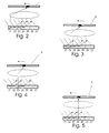
- Figures 2 to 5 is shown as a Data patterns shifted from cell to cell in a row and is stationary on the photosensitive Material 5 remains.
- a signal reaches the first cell Z1.
- the same data pattern is shown in Figure 3 transfer the next column or cell Z2 here, while a new pattern in the first column or here Cell Z1 is transmitted.
- this is the first read data pattern arrived at cell 4 Z4.
- the Cells Z5 to Z6 are not suitable for the device 10 the transmission of the data pattern can be controlled. They stand not to expose the photosensitive material to disposal. Will a higher exposure intensity required, they are activated and the data pattern will be transmitted further.
- Figure 6 shows a light modulator 4, which in rows R1 to R9 and is divided into columns S1 to S8.
- the Cells 11 shown in broken lines represent the Exposure available. Data patterns are in the Read column S8 and transfer it to column S7.
- R1 to R8 is a different one Number of cells 11 controllable. Since the Exposure intensity over the cells of a row is integrated, you get so different Exposure intensities for individual pixels on the photosensitive medium 5.
Landscapes
- Physics & Mathematics (AREA)
- General Physics & Mathematics (AREA)
- Optics & Photonics (AREA)
- Engineering & Computer Science (AREA)
- Theoretical Computer Science (AREA)
- Electromagnetism (AREA)
- General Engineering & Computer Science (AREA)
- Computer Hardware Design (AREA)
- Exposure Of Semiconductors, Excluding Electron Or Ion Beam Exposure (AREA)
- Exposure And Positioning Against Photoresist Photosensitive Materials (AREA)
- Printers Or Recording Devices Using Electromagnetic And Radiation Means (AREA)
- Liquid Crystal (AREA)
- Projection-Type Copiers In General (AREA)
- Apparatus For Radiation Diagnosis (AREA)
- Closed-Circuit Television Systems (AREA)
Description
- Fig. 1:
- eine schematische Darstellung der vollständigen Belichtungs- und Modulationsvorrichtung,
- Fig. 2-5:
- eine schematische Darstellung des Datenmusterübertragungsprinzips und
- Fig. 6:
- eine schematische Darstellung des Lichtmodulators mit für die Belichtung genutzten und ungenutzten Zellen.
Claims (8)
- Belichtungs- und Modulationsvorrichtung (1) zur Modulation der Belichtungsintensität beim Integrating-Digital-Screen-Imaging Verfahren (IDSI) mit einer Lichtquelle (2), mit einem Lichtmodulator (4), der eine Mehrzahl von Reihen aus lichtmodulierenden Zellen (8) aufweist, mit einer Einrichtung (3) zum Abbilden auf dem Lichtmodulator (4), mit einer Einrichtung (9) zum Abbilden des Lichtmodulators (4) auf lichtempfindliches Material (5), mit einer Einrichtung zur Erzeugung einer relativen Bewegung zwischen dem Lichtmodulator (4) und dem lichtempfindlichen Material (5), wobei die Richtung der Bewegung im wesentlichen senkrecht zu der Richtung der Reihen aus lichtmodulierenden Zellen verläuft, sowie mit einer Einrichtung zum Scrollen eines Datenmusters durch die verschiedenen Spalten des Lichtmodulators (4), mit einer Rate, durch die die Abbildung irgend eines Datenmusters im wesentlichen stationär relativ zu den lichtempfindlichen Material (5) während der Bewegung gehalten wird, dadurch gekennzeichnet, daß die Vorrichtung mindestens eine Einrichtung (10) zum Unterbinden des Scrollvorgangs nach einer bestimmten einstellbaren Anzahl der für die Belichtung des lichtempfindlichen Materials (5) genutzten Zellen (11) des Lichtmodulators (4) aufweist.
- Vorrichtung nach Anspruch 1, dadurch gekennzeichnet, daß der Lichtmodulator (4) aus einer Mikrospiegelanordnung (Digital Mirror Device - DMD)besteht.
- Vorrichtung nach Anspruch 3, dadurch gekennzeichnet, daß der Lichtmodulator (4) aus 1024 * 758 Zellen (8) besteht.
- Vorrichtung nach einem der Ansprüche 1 bis 3, dadurch gekennzeichnet, daß der Lichtmodulator (4) aus einer Flüssigkristallanordnung besteht.
- Vorrichtung nach einem der Ansprüche 1 bis 4, dadurch gekennzeichnet, daß der Lichtmodulator (4) aus magnetooptischen Zellen besteht.
- Vorrichtung nach einem der Ansprüche 1 bis 5, dadurch gekennzeichnet, daß der Lichtmodulator (4) aus ferro-elektrischen Zellen besteht.
- Verfahren zur Belichtung und zur Modulation der Belichtungsintensität beim Integrating-Digital-Screen-Imaging Verfahren (IDSI), bei dem Licht aus einer Lichtquelle (2), auf einem Lichtmodulator (4), der eine Mehrzahl von Reihen aus lichtmodulierenden Zellen (8) aufweist, abgebildet wird und von diesem moduliert wird, wonach der Lichtmodulator (4) auf lichtempfindliches Material (5), welches sich in einer Relativbewegung zum Lichtmodulator (4) befindet, abgebildet wird, wobei die Richtung der Bewegung im wesentlichen senkrecht zu der Richtung der Reihen aus lichtmodulierenden Zellen (8) verläuft und daß die auf dem lichtempfindlichen Material (5) abzubildenden Daten durch die Spalten des Lichtmodulators (4) gescrollt werden, mit einer Rate, durch die die Abbildung irgend eines Datenmusters im wesentlichen stationär relativ zu den lichtempfindlichen Material (5) während der Bewegung gehalten wird, dadurch gekennzeichnet, daß der Scrollvorgang, je nach der für den jeweiligen Pixel auf dem zu belichtenden Material vorgesehenen Belichtungszeit, nach einer bestimmten einstellbaren Anzahl der für die Belichtung des lichtempfindlichen Materials (5) genutzten Zellen (11) des Lichtmodulators (4) unterbunden wird.
- Verfahren nach Anspruch 7, dadurch gekennzeichnet, daß die abzubildenden Daten in eine beliebige Spalte verschoben werden können, um von dort aus zu den nächsten folgenden Spalten übertragen zu werden.
Applications Claiming Priority (3)
| Application Number | Priority Date | Filing Date | Title |
|---|---|---|---|
| DE19944760 | 1999-09-17 | ||
| DE19944760A DE19944760A1 (de) | 1999-09-17 | 1999-09-17 | Vorrichtung und Verfahren zur Kompensation von Inhomogenitäten bei Abbildungssystemen |
| PCT/EP2000/007842 WO2001021413A1 (de) | 1999-09-17 | 2000-08-11 | Vorrichtung und verfahren zur kompensation von inhomogenitäten bei abbildungssystemen |
Publications (2)
| Publication Number | Publication Date |
|---|---|
| EP1212198A1 EP1212198A1 (de) | 2002-06-12 |
| EP1212198B1 true EP1212198B1 (de) | 2003-05-14 |
Family
ID=7922467
Family Applications (1)
| Application Number | Title | Priority Date | Filing Date |
|---|---|---|---|
| EP00954624A Expired - Lifetime EP1212198B1 (de) | 1999-09-17 | 2000-08-11 | Vorrichtung und verfahren zur kompensation von inhomogenitäten bei abbildungssystemen |
Country Status (8)
| Country | Link |
|---|---|
| US (1) | US6965364B1 (de) |
| EP (1) | EP1212198B1 (de) |
| JP (1) | JP2004516493A (de) |
| AT (1) | ATE240213T1 (de) |
| CA (1) | CA2383827A1 (de) |
| DE (2) | DE19944760A1 (de) |
| ES (1) | ES2202161T3 (de) |
| WO (1) | WO2001021413A1 (de) |
Cited By (2)
| Publication number | Priority date | Publication date | Assignee | Title |
|---|---|---|---|---|
| WO2006105911A3 (de) * | 2005-04-02 | 2007-04-05 | Punch Graphix Prepress Germany | Belichtungsvorrichtung für druckplatten |
| CN101171548B (zh) * | 2005-04-02 | 2011-03-30 | 赛康Ip有限责任公司 | 用于印版的曝光装置 |
Families Citing this family (21)
| Publication number | Priority date | Publication date | Assignee | Title |
|---|---|---|---|---|
| DE10046518A1 (de) | 2000-09-15 | 2002-04-04 | Fraunhofer Ges Forschung | Verfahren zur Verbesserung der Bildqualität und zur Erhöhung der Schreibgeschwindigkeit bei Belichtung lichtempfindlicher Schichten |
| CN101487982A (zh) * | 2002-08-24 | 2009-07-22 | 无掩模平版印刷公司 | 连续地直接写的光刻技术 |
| US7714983B2 (en) | 2003-09-12 | 2010-05-11 | Carl Zeiss Smt Ag | Illumination system for a microlithography projection exposure installation |
| EP1683077B1 (de) * | 2003-11-03 | 2016-05-25 | Xeikon Prepress NV | Vorrichtung und verfahren zum digitalen belichten |
| US7283209B2 (en) | 2004-07-09 | 2007-10-16 | Carl Zeiss Smt Ag | Illumination system for microlithography |
| US7467939B2 (en) * | 2006-05-03 | 2008-12-23 | 3D Systems, Inc. | Material delivery tension and tracking system for use in solid imaging |
| US7931460B2 (en) * | 2006-05-03 | 2011-04-26 | 3D Systems, Inc. | Material delivery system for use in solid imaging |
| DE102006049169A1 (de) * | 2006-10-18 | 2008-04-30 | Punch Graphix Prepress Germany Gmbh | Beleuchtungsanordnung |
| US20080226346A1 (en) * | 2007-01-17 | 2008-09-18 | 3D Systems, Inc. | Inkjet Solid Imaging System and Method for Solid Imaging |
| US20080170112A1 (en) * | 2007-01-17 | 2008-07-17 | Hull Charles W | Build pad, solid image build, and method for building build supports |
| US20080181977A1 (en) * | 2007-01-17 | 2008-07-31 | Sperry Charles R | Brush assembly for removal of excess uncured build material |
| US7731887B2 (en) * | 2007-01-17 | 2010-06-08 | 3D Systems, Inc. | Method for removing excess uncured build material in solid imaging |
| US8105066B2 (en) * | 2007-01-17 | 2012-01-31 | 3D Systems, Inc. | Cartridge for solid imaging apparatus and method |
| US8003039B2 (en) | 2007-01-17 | 2011-08-23 | 3D Systems, Inc. | Method for tilting solid image build platform for reducing air entrainment and for build release |
| US7706910B2 (en) * | 2007-01-17 | 2010-04-27 | 3D Systems, Inc. | Imager assembly and method for solid imaging |
| US7771183B2 (en) * | 2007-01-17 | 2010-08-10 | 3D Systems, Inc. | Solid imaging system with removal of excess uncured build material |
| US7614866B2 (en) * | 2007-01-17 | 2009-11-10 | 3D Systems, Inc. | Solid imaging apparatus and method |
| US8221671B2 (en) * | 2007-01-17 | 2012-07-17 | 3D Systems, Inc. | Imager and method for consistent repeatable alignment in a solid imaging apparatus |
| US9034237B2 (en) | 2012-09-25 | 2015-05-19 | 3D Systems, Inc. | Solid imaging systems, components thereof, and methods of solid imaging |
| CN103412467B (zh) * | 2013-08-12 | 2015-07-01 | 中山新诺科技有限公司 | 沿扫描方向进行均匀性补偿装置及利用该装置进行均匀性补偿方法 |
| KR102396288B1 (ko) * | 2014-10-27 | 2022-05-10 | 삼성디스플레이 주식회사 | 유기 발광 표시 장치 |
Family Cites Families (9)
| Publication number | Priority date | Publication date | Assignee | Title |
|---|---|---|---|---|
| US5049901A (en) * | 1990-07-02 | 1991-09-17 | Creo Products Inc. | Light modulator using large area light sources |
| CA2075026A1 (en) * | 1991-08-08 | 1993-02-09 | William E. Nelson | Method and apparatus for patterning an imaging member |
| US5247180A (en) * | 1991-12-30 | 1993-09-21 | Texas Instruments Incorporated | Stereolithographic apparatus and method of use |
| US5510824A (en) * | 1993-07-26 | 1996-04-23 | Texas Instruments, Inc. | Spatial light modulator array |
| US5844588A (en) * | 1995-01-11 | 1998-12-01 | Texas Instruments Incorporated | DMD modulated continuous wave light source for xerographic printer |
| US6072518A (en) * | 1997-05-21 | 2000-06-06 | Creo Products Inc. | Method for rapid imaging of thermographic materials by extending exposure time in a single beam laser scanner |
| IL119099A (en) * | 1996-08-20 | 1999-05-09 | Scitex Corp Ltd | Apparatus and method for recording an image |
| US6233036B1 (en) * | 1998-01-20 | 2001-05-15 | Citizen Watch Co., Ltd. | Optical printer |
| DE19830896A1 (de) * | 1998-07-10 | 2000-06-08 | Mivatec Gmbh | Fotoplott-Verfahren zur hochenergetischen Aufzeichnung eines computergespeicherten Rasterbildes auf einen lichtempfindlichen Aufzeichnungsträger |
-
1999
- 1999-09-17 DE DE19944760A patent/DE19944760A1/de not_active Withdrawn
-
2000
- 2000-08-11 JP JP2001524812A patent/JP2004516493A/ja active Pending
- 2000-08-11 US US10/070,709 patent/US6965364B1/en not_active Expired - Fee Related
- 2000-08-11 DE DE50002207T patent/DE50002207D1/de not_active Expired - Lifetime
- 2000-08-11 CA CA002383827A patent/CA2383827A1/en not_active Abandoned
- 2000-08-11 AT AT00954624T patent/ATE240213T1/de not_active IP Right Cessation
- 2000-08-11 WO PCT/EP2000/007842 patent/WO2001021413A1/de not_active Ceased
- 2000-08-11 EP EP00954624A patent/EP1212198B1/de not_active Expired - Lifetime
- 2000-08-11 ES ES00954624T patent/ES2202161T3/es not_active Expired - Lifetime
Cited By (2)
| Publication number | Priority date | Publication date | Assignee | Title |
|---|---|---|---|---|
| WO2006105911A3 (de) * | 2005-04-02 | 2007-04-05 | Punch Graphix Prepress Germany | Belichtungsvorrichtung für druckplatten |
| CN101171548B (zh) * | 2005-04-02 | 2011-03-30 | 赛康Ip有限责任公司 | 用于印版的曝光装置 |
Also Published As
| Publication number | Publication date |
|---|---|
| ATE240213T1 (de) | 2003-05-15 |
| EP1212198A1 (de) | 2002-06-12 |
| US6965364B1 (en) | 2005-11-15 |
| DE50002207D1 (de) | 2003-06-18 |
| ES2202161T3 (es) | 2004-04-01 |
| JP2004516493A (ja) | 2004-06-03 |
| CA2383827A1 (en) | 2001-03-29 |
| WO2001021413A1 (de) | 2001-03-29 |
| DE19944760A1 (de) | 2001-03-22 |
Similar Documents
| Publication | Publication Date | Title |
|---|---|---|
| DE19944760A1 (de) | Vorrichtung und Verfahren zur Kompensation von Inhomogenitäten bei Abbildungssystemen | |
| DE69421241T2 (de) | Schemata mit kombinierten Modulatoren für räumliche Lichtmodulatoren | |
| DE69424604T2 (de) | Räumliche Lichtmodulation | |
| DE69321381T2 (de) | Drucker mit verformbarer Matrixspiegelvorrichtung (DMD) | |
| DE3882358T2 (de) | System zur multiplexierten belichtung eines feldes mit regionen, deren belichtung gleichwinklig abgelenkt ist. | |
| DE69420892T2 (de) | Optisches Gerät | |
| DE69615939T2 (de) | Verbesserungen für das Grautondrucken mit räumlichen Lichtmodulatoren | |
| DE69526696T2 (de) | Lichtmodulator mit einer Laseranordnung zum Darstellen von Bilddaten | |
| DE4121509A1 (de) | Belichtungs- und lichtmodulationssystem | |
| DE69016473T2 (de) | Farbvideodrucker. | |
| DE3212194C2 (de) | ||
| DE69225442T2 (de) | Verfahren zur Kalibrierung eines Mehrkanal-Druckers | |
| DE60217034T2 (de) | Bildaufzeichnungsverfahren und -Vorrichtung | |
| DE10296370B4 (de) | Belichtungsvorrichtung für Lasersysteme | |
| DE3881866T2 (de) | System zur belichtungsadressierung hoher auflösung mit grobaufgelöstem belichtungsfeld. | |
| DE19545625C1 (de) | Verfahren und Vorrichtung zur Aufzeichnung von Bildern mittels elektronischer Bildsignale | |
| DE3883744T2 (de) | Vielfarbige lichtventilabbildungsvorrichtung mit elektrodenkonstruktion zur gleichförmigen übertragung. | |
| DE69503326T2 (de) | Verfahren und Gerät zum Schreiben auf ein lichtempfindliches Material mittels eines modulierten Lichtstrahles | |
| EP1189425B1 (de) | Mehrstrahl-Belichtungsverfahren | |
| DE69530655T2 (de) | Druckverfahren und Drucker unter Verwendung eines räumlichen Modulators | |
| EP1683077A1 (de) | Vorrichtung und verfahren zum digitalen belichten | |
| EP1380885A1 (de) | Vorrichtung und Verfahren zum Aufbelichten von digitalisierten Bildinformationen auf ein lichtempfindliches Material | |
| EP0477441A1 (de) | Verfahren zum Formen von Buchstaben für die Herstellung von Halbton-Tiefdruckplatten | |
| DE4139407C2 (de) | Vorrichtung und Verfahren zum Erzeugen von Bilddarstellungen in einem Farbvideodrucker | |
| EP2183114B1 (de) | Verfahren zur steigerung des durchsatzes und zur reduzierung der bewegungsunschärfe |
Legal Events
| Date | Code | Title | Description |
|---|---|---|---|
| PUAI | Public reference made under article 153(3) epc to a published international application that has entered the european phase |
Free format text: ORIGINAL CODE: 0009012 |
|
| 17P | Request for examination filed |
Effective date: 20020122 |
|
| AK | Designated contracting states |
Kind code of ref document: A1 Designated state(s): AT BE CH CY DE DK ES FI FR GB GR IE IT LI LU MC NL PT SE |
|
| GRAH | Despatch of communication of intention to grant a patent |
Free format text: ORIGINAL CODE: EPIDOS IGRA |
|
| GRAH | Despatch of communication of intention to grant a patent |
Free format text: ORIGINAL CODE: EPIDOS IGRA |
|
| GRAA | (expected) grant |
Free format text: ORIGINAL CODE: 0009210 |
|
| AK | Designated contracting states |
Designated state(s): AT BE CH CY DE DK ES FI FR GB GR IE IT LI LU MC NL PT SE |
|
| PG25 | Lapsed in a contracting state [announced via postgrant information from national office to epo] |
Ref country code: FI Free format text: LAPSE BECAUSE OF FAILURE TO SUBMIT A TRANSLATION OF THE DESCRIPTION OR TO PAY THE FEE WITHIN THE PRESCRIBED TIME-LIMIT Effective date: 20030514 Ref country code: IE Free format text: LAPSE BECAUSE OF FAILURE TO SUBMIT A TRANSLATION OF THE DESCRIPTION OR TO PAY THE FEE WITHIN THE PRESCRIBED TIME-LIMIT Effective date: 20030514 |
|
| REG | Reference to a national code |
Ref country code: GB Ref legal event code: FG4D Free format text: NOT ENGLISH |
|
| REG | Reference to a national code |
Ref country code: CH Ref legal event code: EP |
|
| REG | Reference to a national code |
Ref country code: IE Ref legal event code: FG4D Free format text: GERMAN |
|
| REF | Corresponds to: |
Ref document number: 50002207 Country of ref document: DE Date of ref document: 20030618 Kind code of ref document: P |
|
| GBT | Gb: translation of ep patent filed (gb section 77(6)(a)/1977) | ||
| REG | Reference to a national code |
Ref country code: CH Ref legal event code: NV Representative=s name: PATENTANWALTSBUERO PETSCHNER & PARTNER |
|
| PG25 | Lapsed in a contracting state [announced via postgrant information from national office to epo] |
Ref country code: AT Free format text: LAPSE BECAUSE OF NON-PAYMENT OF DUE FEES Effective date: 20030811 Ref country code: CY Free format text: LAPSE BECAUSE OF FAILURE TO SUBMIT A TRANSLATION OF THE DESCRIPTION OR TO PAY THE FEE WITHIN THE PRESCRIBED TIME-LIMIT Effective date: 20030811 |
|
| PG25 | Lapsed in a contracting state [announced via postgrant information from national office to epo] |
Ref country code: GR Free format text: LAPSE BECAUSE OF FAILURE TO SUBMIT A TRANSLATION OF THE DESCRIPTION OR TO PAY THE FEE WITHIN THE PRESCRIBED TIME-LIMIT Effective date: 20030814 Ref country code: PT Free format text: LAPSE BECAUSE OF FAILURE TO SUBMIT A TRANSLATION OF THE DESCRIPTION OR TO PAY THE FEE WITHIN THE PRESCRIBED TIME-LIMIT Effective date: 20030814 Ref country code: DK Free format text: LAPSE BECAUSE OF FAILURE TO SUBMIT A TRANSLATION OF THE DESCRIPTION OR TO PAY THE FEE WITHIN THE PRESCRIBED TIME-LIMIT Effective date: 20030814 Ref country code: SE Free format text: LAPSE BECAUSE OF FAILURE TO SUBMIT A TRANSLATION OF THE DESCRIPTION OR TO PAY THE FEE WITHIN THE PRESCRIBED TIME-LIMIT Effective date: 20030814 |
|
| PG25 | Lapsed in a contracting state [announced via postgrant information from national office to epo] |
Ref country code: MC Free format text: LAPSE BECAUSE OF NON-PAYMENT OF DUE FEES Effective date: 20030831 |
|
| REG | Reference to a national code |
Ref country code: IE Ref legal event code: FD4D Ref document number: 1212198E Country of ref document: IE |
|
| ET | Fr: translation filed | ||
| PLBE | No opposition filed within time limit |
Free format text: ORIGINAL CODE: 0009261 |
|
| STAA | Information on the status of an ep patent application or granted ep patent |
Free format text: STATUS: NO OPPOSITION FILED WITHIN TIME LIMIT |
|
| REG | Reference to a national code |
Ref country code: ES Ref legal event code: FG2A Ref document number: 2202161 Country of ref document: ES Kind code of ref document: T3 |
|
| 26N | No opposition filed |
Effective date: 20040217 |
|
| REG | Reference to a national code |
Ref country code: CH Ref legal event code: PCAR Representative=s name: PATENTANWALTSBUERO URSULA RENFER-VONNEMANN;ROSWIESENSTRASSE 61;8309 BIRCHWIL-NUERENSDORF (CH) |
|
| REG | Reference to a national code |
Ref country code: CH Ref legal event code: PUE Owner name: BASYS PRINT GMBH SYSTEME FUER DIE DRUCKINDUSTRIE Free format text: BASYS PRINT GMBH SYSTEME FUER DIE DRUCKINDUSTRIE#GUELZER STRASSE 15#19258 BOIZENBURG (DE) $ TOYO INK. MFG. CO. LTD.#21-1, KAGA, 1-CHOME, ITAHASHI-KU#TOKYO 173-8666 (JP) -TRANSFER TO- BASYS PRINT GMBH SYSTEME FUER DIE DRUCKINDUSTRIE#GUELZER STRASSE 15#19258 BOIZENBURG (DE) |
|
| REG | Reference to a national code |
Ref country code: GB Ref legal event code: 732E |
|
| REG | Reference to a national code |
Ref country code: ES Ref legal event code: PC2A |
|
| NLS | Nl: assignments of ep-patents |
Owner name: BASYS PRINT GMBH SYSTEME FUER DIE DRUCKINDUSTRIE Effective date: 20051108 |
|
| REG | Reference to a national code |
Ref country code: FR Ref legal event code: TP |
|
| REG | Reference to a national code |
Ref country code: FR Ref legal event code: CD |
|
| NLT1 | Nl: modifications of names registered in virtue of documents presented to the patent office pursuant to art. 16 a, paragraph 1 |
Owner name: PUNCH GRAPHIX PREPRESS GERMANY GMBH |
|
| REG | Reference to a national code |
Ref country code: CH Ref legal event code: PFA Owner name: PUNCH GRAPHIX PREPRESS GERMANY GMBH Free format text: BASYS PRINT GMBH SYSTEME FUER DIE DRUCKINDUSTRIE#GUELZER STRASSE 15#19258 BOIZENBURG (DE) -TRANSFER TO- PUNCH GRAPHIX PREPRESS GERMANY GMBH#GUELZER STRASSE 15#19258 BOIZENBURG (DE) |
|
| REG | Reference to a national code |
Ref country code: ES Ref legal event code: PC2A |
|
| BECA | Be: change of holder's address |
Owner name: *PUNCH GRAPHIX PREPRESS GERMANY G.M.B.H.G?LZER STR Effective date: 20060309 |
|
| BECN | Be: change of holder's name |
Owner name: *PUNCH GRAPHIX PREPRESS GERMANY G.M.B.H.G?LZER STR Effective date: 20060309 |
|
| REG | Reference to a national code |
Ref country code: CH Ref legal event code: NV Representative=s name: KATZAROV S.A. |
|
| REG | Reference to a national code |
Ref country code: GB Ref legal event code: 732E Free format text: REGISTERED BETWEEN 20100225 AND 20100303 |
|
| REG | Reference to a national code |
Ref country code: FR Ref legal event code: TP |
|
| REG | Reference to a national code |
Ref country code: CH Ref legal event code: PUE Owner name: XEIKON IP BV Free format text: PUNCH GRAPHIX PREPRESS GERMANY GMBH#GUELZER STRASSE 15#19258 BOIZENBURG (DE) -TRANSFER TO- XEIKON IP BV#BRIEVERSSTRAAT 70#4529 GZ EEDE (NL) |
|
| REG | Reference to a national code |
Ref country code: ES Ref legal event code: PC2A |
|
| REG | Reference to a national code |
Ref country code: NL Ref legal event code: SD Effective date: 20100922 |
|
| PGFP | Annual fee paid to national office [announced via postgrant information from national office to epo] |
Ref country code: CH Payment date: 20110824 Year of fee payment: 12 |
|
| PGFP | Annual fee paid to national office [announced via postgrant information from national office to epo] |
Ref country code: LU Payment date: 20120824 Year of fee payment: 13 |
|
| PGFP | Annual fee paid to national office [announced via postgrant information from national office to epo] |
Ref country code: ES Payment date: 20120816 Year of fee payment: 13 Ref country code: BE Payment date: 20120824 Year of fee payment: 13 Ref country code: IT Payment date: 20120821 Year of fee payment: 13 |
|
| PGFP | Annual fee paid to national office [announced via postgrant information from national office to epo] |
Ref country code: NL Payment date: 20120821 Year of fee payment: 13 |
|
| BERE | Be: lapsed |
Owner name: XEIKON IP B.V. Effective date: 20130831 |
|
| REG | Reference to a national code |
Ref country code: NL Ref legal event code: V1 Effective date: 20140301 |
|
| REG | Reference to a national code |
Ref country code: CH Ref legal event code: PL |
|
| PG25 | Lapsed in a contracting state [announced via postgrant information from national office to epo] |
Ref country code: LI Free format text: LAPSE BECAUSE OF NON-PAYMENT OF DUE FEES Effective date: 20130831 Ref country code: NL Free format text: LAPSE BECAUSE OF NON-PAYMENT OF DUE FEES Effective date: 20140301 Ref country code: CH Free format text: LAPSE BECAUSE OF NON-PAYMENT OF DUE FEES Effective date: 20130831 |
|
| PG25 | Lapsed in a contracting state [announced via postgrant information from national office to epo] |
Ref country code: IT Free format text: LAPSE BECAUSE OF NON-PAYMENT OF DUE FEES Effective date: 20130811 Ref country code: BE Free format text: LAPSE BECAUSE OF NON-PAYMENT OF DUE FEES Effective date: 20130831 |
|
| REG | Reference to a national code |
Ref country code: ES Ref legal event code: FD2A Effective date: 20141010 |
|
| PG25 | Lapsed in a contracting state [announced via postgrant information from national office to epo] |
Ref country code: ES Free format text: LAPSE BECAUSE OF NON-PAYMENT OF DUE FEES Effective date: 20130812 |
|
| PG25 | Lapsed in a contracting state [announced via postgrant information from national office to epo] |
Ref country code: LU Free format text: LAPSE BECAUSE OF NON-PAYMENT OF DUE FEES Effective date: 20130811 |
|
| REG | Reference to a national code |
Ref country code: FR Ref legal event code: PLFP Year of fee payment: 16 |
|
| REG | Reference to a national code |
Ref country code: DE Ref legal event code: R082 Ref document number: 50002207 Country of ref document: DE Representative=s name: VONNEMANN, KLOIBER & KOLLEGEN, DE Ref country code: DE Ref legal event code: R081 Ref document number: 50002207 Country of ref document: DE Owner name: XEIKON PREPRESS NV, BE Free format text: FORMER OWNER: XEIKON IP BV, EEDE, NL Ref country code: DE Ref legal event code: R082 Ref document number: 50002207 Country of ref document: DE Representative=s name: VKK PATENTANWAELTE, DE |
|
| REG | Reference to a national code |
Ref country code: GB Ref legal event code: 732E Free format text: REGISTERED BETWEEN 20160104 AND 20160106 |
|
| REG | Reference to a national code |
Ref country code: FR Ref legal event code: TP Owner name: XEIKON PREPRESS NV, BE Effective date: 20160112 |
|
| REG | Reference to a national code |
Ref country code: FR Ref legal event code: PLFP Year of fee payment: 17 |
|
| PGFP | Annual fee paid to national office [announced via postgrant information from national office to epo] |
Ref country code: DE Payment date: 20160822 Year of fee payment: 17 Ref country code: GB Payment date: 20160819 Year of fee payment: 17 |
|
| PGFP | Annual fee paid to national office [announced via postgrant information from national office to epo] |
Ref country code: FR Payment date: 20160822 Year of fee payment: 17 |
|
| REG | Reference to a national code |
Ref country code: DE Ref legal event code: R119 Ref document number: 50002207 Country of ref document: DE |
|
| GBPC | Gb: european patent ceased through non-payment of renewal fee |
Effective date: 20170811 |
|
| REG | Reference to a national code |
Ref country code: FR Ref legal event code: ST Effective date: 20180430 |
|
| PG25 | Lapsed in a contracting state [announced via postgrant information from national office to epo] |
Ref country code: DE Free format text: LAPSE BECAUSE OF NON-PAYMENT OF DUE FEES Effective date: 20180301 Ref country code: GB Free format text: LAPSE BECAUSE OF NON-PAYMENT OF DUE FEES Effective date: 20170811 |
|
| PG25 | Lapsed in a contracting state [announced via postgrant information from national office to epo] |
Ref country code: FR Free format text: LAPSE BECAUSE OF NON-PAYMENT OF DUE FEES Effective date: 20170831 |