EP1211462B1 - Zündschaltung zur Versorgung einer Zündelektrode - Google Patents
Zündschaltung zur Versorgung einer Zündelektrode Download PDFInfo
- Publication number
- EP1211462B1 EP1211462B1 EP20010127984 EP01127984A EP1211462B1 EP 1211462 B1 EP1211462 B1 EP 1211462B1 EP 20010127984 EP20010127984 EP 20010127984 EP 01127984 A EP01127984 A EP 01127984A EP 1211462 B1 EP1211462 B1 EP 1211462B1
- Authority
- EP
- European Patent Office
- Prior art keywords
- transistor
- capacitor
- circuit
- thyristor
- ignition
- Prior art date
- Legal status (The legal status is an assumption and is not a legal conclusion. Google has not performed a legal analysis and makes no representation as to the accuracy of the status listed.)
- Expired - Lifetime
Links
- 239000003990 capacitor Substances 0.000 claims description 25
- 238000007599 discharging Methods 0.000 description 2
- 238000004804 winding Methods 0.000 description 2
- 230000015572 biosynthetic process Effects 0.000 description 1
- 230000000903 blocking effect Effects 0.000 description 1
- 230000015556 catabolic process Effects 0.000 description 1
- 238000010304 firing Methods 0.000 description 1
- 230000001960 triggered effect Effects 0.000 description 1
Images

Classifications
-
- F—MECHANICAL ENGINEERING; LIGHTING; HEATING; WEAPONS; BLASTING
- F23—COMBUSTION APPARATUS; COMBUSTION PROCESSES
- F23Q—IGNITION; EXTINGUISHING-DEVICES
- F23Q3/00—Igniters using electrically-produced sparks
- F23Q3/004—Using semiconductor elements
Definitions
- the invention relates to an ignition circuit according to the preamble of the independent claim.
- the ignition frequency is usually generated via an R-C combination in conjunction with a Diac, which causes the trigger pulse (ignition pulse) for the discharge of a capacitor via a thyristor as a switch through the primary winding of a transformer when the breakdown voltage is exceeded.
- the thyrister is fired by a trigger pulse generated by a logic circuit or a ⁇ P controller.
- the DE 2 336 192 A discloses an electronic ignition device for gas appliances, according to the preamble of claim 1, wherein a pulse signal for blocking a thyristor and thus leads to a discharge of a capacitor. While the ignition is done electronically, the power supply must be interrupted by a push button to switch off the ignition.
- the aim of the invention is to avoid the disadvantages of the prior art and to propose an ignition circuit of the type mentioned, which is characterized by a simple structure.
- the proposed measures can be dispensed with a network frequency converting circuit, as provided in the known solutions.
- the proposed solution is characterized by a very simple structure.
- the proposed measures ensures that shortly before the start of a depending on the type of the trigger terminal of the thyristor controlling transistor negative or positive half wave of the supply voltage an ignition pulse for the thyristor is triggered by the transistor. This leads to a transhipment of the series connected to the primary coil of the transformer capacitor and thus to a current flow through the primary coil.
- the ignition is switched off and on by switching the supply voltage or by switching the trigger pulse for the thyristor.
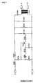
- FIG. 1 and 2 show two different embodiments of an ignition circuit according to the invention.
- a resistor R100 is connected to a mains connection L, to which a diode D100 is connected downstream.
- the second network connection N is a thyristor T100, a parallel to this resistor R101, connected to this parallel freewheeling diode D101 and also connected in parallel series connection.
- This series connection is formed by a primary coil 1 of a transformer U100 and a capacitor C100.
- ignition electrodes Z1, Z2 are connected, which are arranged in the region of a gas burner, not shown.
- a voltage divider circuit Connected between the resistor R100 and the diode D100 is a voltage divider circuit connected to the second mains terminal N, which is formed by the resistors R106 and R110.
- the base of a pnp transistor T101 and a series circuit formed of a diode D102 and a resistor R114 are connected.
- the emitter of the transistor T101 and a capacitor C101 is connected to this series circuit, which is connected to the second network terminal N.
- the collector of the transistor T101 is connected via a resistor R102 to the gate terminal of the thyristor T101.
- FIG. 2 differs from that of FIG. 1 in that a further transistor T102 is connected in parallel with the capacitor C101 which is connected to the emitter of the transistor T101.
- the base of this transistor T102 is connected, on the one hand, via a resistor R113 to the diode D102 and to the resistor R114 connected in series therewith, and to an optocoupler IC100 whose main current element or emitter is connected to the second network connection N.
- the control input of the optocoupler IC100 is connected via a resistor R112 to a control voltage UB, wherein the light-emitting diode of the optocoupler IC100 is further connected to a control terminal OFF.
- the trigger pulse for the thyristor T100 which is used to control the transformer U100, generated shortly before the start of each negative half cycle of the AC supply voltage between the power terminals L and N.
- the spark between the ignition electrode Z1 and the ignition electrode 2 is generated by discharging a capacitor C100 through the primary winding of a transformer U100.
- the switching element used here is the thyristor T100, the diode D101, which is connected in parallel therewith, serving as a freewheeling diode.
- the resistor R101 discharges the capacitor C100 after turning off the power supply.
- the capacitor C100 is charged via the resistor R100 and the diode D100.
- the energy required for the ignition pulse, which is transmitted to the electrodes via the transformer U100, is then stored in the capacitor C100.
- the capacitor C101 is charged via the resistors R100 and R106, the diode D102 and the resistor R114. Via the voltage divider, which is formed by the resistors R100 and R106, on the one hand, and the resistor R110, the voltage across the capacitor C101 is limited.
- the transistor T101 turns off because the base potential of the PNP transistor is above its emitter potential. With the end of the positive half cycle of the supply voltage, the base potential becomes smaller than the emitter potential of the transistor T101, which is kept at a positive potential by the capacitor C101. The transistor T101 therefore becomes conductive and remains in this switching state during the negative half cycle of the supply voltage.
- the capacitor C101 discharges through the resistor R102 into the trigger terminal of the thyristor T100 and ignites it.
- the capacitor C100 is discharged via the primary coil 1 of the transformer U100.
- the Voltage pulse is up-transformed via the secondary coil 2 of the transformer U100 and between the two ignition electrodes Z1, Z2 forms a spark gap.
- FIG. 2 shows by way of example how the formation of an ignition pulse can be prevented by shorting the capacitor C101, which is possible by the transistor T102 connected in parallel therewith.
- the ignition can also be switched on and off by switching the supply AC voltage L N via a relay or an Optotriac.
- the transistor T102 is switched via an opto-coupler IC100, wherein the base of the transistor T102 via the resistor R113 in non-switched optocoupler IC100 during the positive half-wave of the supply voltage on a higher compared to the emitter of the transistor T101 Potential is maintained and therefore turned on and therefore the capacitor C101 can not charge.
- the transistor T101 can indeed switch through, but the thyristor T100 can not be ignited because C101 can discharge via R102.
- the capacitor C100 can not discharge.
- the proposed ignition circuits are characterized by only a few, simple components and thus a small footprint, as well as high reliability.
Landscapes
- Engineering & Computer Science (AREA)
- Chemical & Material Sciences (AREA)
- Combustion & Propulsion (AREA)
- Mechanical Engineering (AREA)
- General Engineering & Computer Science (AREA)
- Ignition Installations For Internal Combustion Engines (AREA)
Description
- Die Erfindung bezieht sich auf eine Zündschaltung gemäß dem Oberbegriff des unabhängigen Anspruches.
- Bei den derzeit eingesetzten Zünderschaltungen wird die Zündfrequenz meist über eine R-C-Kombination in Verbindung mit einem Diac erzeugt, der bei Überschreiten der Durchbruchspannung den Triggerimpuls (Zündimpuls) für die Entladung eines Kondensators über einen Thyristor als Schalter durch die Primärwicklung eines Übertragers bewirkt. In anderen Schaltungen wird der Thyrister durch einen Triggerimpuls gezündet, der durch einen Logikschaltkreis oder einen µP-Controller erzeugt wird.
- Bei den bekannten derartigen Schaltungen wird in der Regel mit einer relativ hohen Frequenz gearbeitet, wodurch sich jedoch der Nachteil großer Toleranzen der Zündfrequenz und -spannung bei Diacs und der große Abstand durch das notwendige Vorhandensein einer Logigschaltung bei µP-Controllern ergibt.
- Die
DE 2 336 192 A offenbart eine elektronische Zündeinrichtung für Gasgeräte, nach dem Oberbegriff des Anspruchs 1, bei welcher ein Impulssignal zur Sperrung eines Thyristors und damit zu einer Entladung eines Kondensators führt. Während die Zündung elektronisch erfolgt, muss zum Abschalten der Zündeinrichtung die Stromversorgung durch einen Druckknopf unterbrochen werden. - Ziel der Erfindung ist es, die Nachteile des Standes der Technik zu vermeiden und eine Zündschaltung der eingangs erwähnten Art vorzuschlagen, die sich durch einen einfachen Aufbau auszeichnet.
- Erfindungsgemäß wird dies bei einer Zündschaltung der eingangs erwähnten Art durch die kennzeichnenden Merkmale des unabhängigen Anspruches erreicht.
- Durch die vorgeschlagenen Maßnahmen kann auf eine die Netzfrequenz umsetzende Schaltung, wie sie bei den bekannten Lösungen vorgesehen sind, verzichtet werden. Außerdem zeichnet sich die vorgeschlagene Lösung durch einen sehr einfachen Aufbau aus.
- Durch die vorgeschlagenen Maßnahmen ist sichergestellt, daß kurz vor Beginn einer je nach Typ des den Triggeranschluß des Thyristors steuernden Transistors negativen oder positiven Halbwelle der Versorgungsspannung ein Zündimpuls für den Thyristor durch den Transistor ausgelöst wird. Dadurch kommt es zu einer Umladung des in Reihe zur Primärspule des Übertragers geschalteten Kondensators und damit zu einem Stromfluß über die Primärspule.
- Die Zündung wird dabei durch Schalten der Versorgungsspannung oder durch Schalten des Triggerimpulses für den Thyristor aus- und eingeschaltet.
- Die Erfindung wird nun anhand der Zeichnung näher erläutert. Dabei zeigen die Fig. 1 und 2 zwei verschiedene Ausführungsformen einer erfindungsgemäßen Zündschaltung.
- Gleiche Bezugszeichen bedeuten in beiden Figuren gleiche Einzelteile.
- Bei der Ausführungsform nach der Fig. 1 ist an einen Netzanschluß L ein Widerstand R100 angeschlossen, dem eine Diode D100 nachgeschaltet ist. An diese und dem zweiten Netzanschluß N ist ein Thyristor T100, ein zu diesem parallel geschalteter Widerstand R101, eine zu diesem parallel geschaltete Freilaufdiode D101 und eine ebenfalls parallgeschaltete Reihenschaltung angeschlossen. Diese Reihenschaltung ist durch eine Primärspule 1 eines Übertragers U100 und einen Kondensator C100 gebildet.
- An die Sekundärspule 2 des Übertragers U100 sind Zündelektroden Z1, Z2 angeschlossen, die im Bereich eines nicht dargestellten Gasbrenners angeordnet sind.
- Zwischen dem Widerstand R100 und der Diode D100 ist eine mit dem zweiten Netzanschluß N verbundene Spannungsteilerschaltung angeschlossen, die durch die Widerstände R106 und R110 gebildet ist. An der Verbindung dieser beiden Widerstände R106 und R110 ist die Basis eines pnp-Transistors T101 und eine aus einer Diode D102 und einem Widerstand R114 gebildete Reihenschaltung angeschlossen. Dabei ist an diese Reihenschaltung der Emitter des Transistors T101 und ein Kondensator C101 angeschlossen, der mit dem zweiten Netzanschluß N verbunden ist.
- Der Kollektor des Transistors T101 ist über einen Widerstand R102 mit dem Gateanschluß des Thyristors T101 verbunden.
- Die Ausführungsform nach der Fig. 2 unterscheidet sich von jener nach der Fig. 1 dadurch, daß parallel zum Kondensator C101, der mit dem Emitter des Transistors T101 verbunden ist, ein weiterer Transistor T102 parallel geschaltet ist. Dabei ist die Basis dieses Transistors T102 einerseits über einen Widerstand R113 mit der Diode D102 und dem zu dieser in Reihe geschalteten Widerstand R114 und mit einem Optokoppler IC100 verbunden, dessen Hauptstromstecke, bzw. Emitter mit dem zweiten Netzanschluß N verbunden ist.
- Der Steuereingang des Optokopplers IC100 ist über einen Widerstand R112 mit einer Steuerspannung UB verbunden, wobei die Leuchtdiode des Optokopplers IC100 weiter mit einem Steueranschluß OFF verbunden ist.
- Bei der Zünderschaltung nach der Fig. 1 und 2 wird der Triggerimpuls für den Thyristor T100, der zur Steuerung des Übertragers U100 dient, kurz vor Beginn jeder negativen Halbwelle der Versorgungs-Wechselspannung zwischen den Netzanschlüssen L und N erzeugt.
- Der Zündfunke zwischen der Zündelektrode Z1 und der Zündelektrode 2 wird durch Entladung eines Kondensators C100 durch die Primärwicklung eines Übertragers U100 erzeugt. Als Schaltelement dient dabei der Thyristor T100, wobei die zu diese, parallel geschaltete Diode D101 als Freilaufdiode dient. Der Widerstand R101 entlädt den Kondensator C100 nach dem Abschalten der Spannungsversorgung.
- Während der positiven Halbwelle der Versorgungsspannung wird über den Widerstand R100 und die Diode D100 der Kondensator C100 geladen. Die benötigte Energie für den Zündimpuls, der über den Übertrager U100 auf die Elektroden übertragen wird, ist dann im Kondensator C100 gespeichert.
- Gleichzeitig wird über die Widerstände R100 und R106, die Diode D102 und den Widerstand R114 der Kondensator C101 geladen. Über den Spannungsteiler, der durch die Widerstände R100 und R106 einerseits und den Widerstand R110 gebildet ist, wird die Spannung an dem Kondensator C101 begrenzt. Während der Ladezeit des Kondensators C101 sperrt der Transistor T101, da das Basispotential des pnp-Transistors über dessen Emitterpotential liegt. Mit Ende der positiven Halbwelle der Versorgungsspannung wird das Basispotential kleiner als das Emitterpotential des Transistors T101, das durch den Kondensator C101 auf positivem Potential gehalten wird. Der Transistor T101 wird daher leitend und bleibt in diesem Schaltzustand während der negativen Halbwelle der Versorgungsspannung.
- Dies führt dazu, daß der Kondensator C101 sich über den Widerstand R102 in den Triggeranschluß des Thyristors T100 entlädt und diesen zündet. Jetzt wird, wie oben erwähnt, der Kondensator C100 über die Primärspule 1 des Übertragers U100 entladen. Der Spannungsimpuls wird über die Sekundärspule 2 des Übertragers U100 hochtransformiert und zwischen den beiden Zündelektroden Z1, Z2 bildet sich eine Funkenstrecke aus.
- In Fig.2 ist beispielhaft dargestellt, wie durch Kurzschließen des Kondensators C101, was durch den zu diesem parallel geschalteten Transistor T102 möglich ist, die Ausbildung eines Zündimpulses unterbunden werden kann. Die Zündung kann natürlich auch durch Schalten der Versorgungs-Wechselspannung L N über ein Relais oder einen Optotriac ebenfalls ein- und ausgeschaltet werden.
- Bei dem in der Fig. 2 dargestellten Ausführungsbeispiel erfolgt das Schalten des Transistors T102 über einen Optokoppler IC100, wobei die Basis des Transistors T102 über den Widerstand R113 bei nicht durchgeschaltetem Optokoppler IC100 während der positiven Halbwelle der Versorgungsspannung auf einem gegenüber dem Emitter des Transistors T101 höheren Potential gehalten ist und daher leitend geschaltet ist und sich daher der Kondensator C101 nicht aufladen kann. Damit kann bei der folgenden negativen Halbwelle der Versorgungsspannung der Transistor T101 zwar durchschalten, aber der Thyristor T100 kann nicht gezündet werden, da sich C101 über R102 entladen kann. Somit kann sich auch der Kondensator C100 nicht entladen.
- Wird dagegen der Steueranschluß OFF an Masse gelegt, so kommt es zu einem Stromfluß über die Leuchtdiode des Optokopplers IC100 und dieser schaltet durch, wodurch die Basis des Transistors T102 im wesentlichen auf das Potential dessen Emitters gelegt wird und der Transistor T102 sperrt. Dadurch kann sich der Kondensator C101 während der positiven Halbwelle aufladen und der Transistor T101 während der folgenden negativen Halbwelle durchschalten und durch Entladen von C101 einen Zündimpuls auslösen.
- Die vorgeschlagenen Zündschaltungen zeichnen sich durch nur wenige, einfache Bauteile und damit einen geringen Platzbedarf, sowie einer hohe Zuverlässigkeit aus.
Claims (1)
- Zündschaltung zur Versorgung einer Zündelektrode, insbesondere für die Zündung einer Gasflamme, bei welcher Zündschaltung einen Übertrager (U100) aufweist, dessen Primärspule (1) über eine Impulsgeberschaltung ansteuerbar ist, wobei die Zündelektrode (Z1, Z2) an die Sekundärspule (2) des Übertragers (U100) angeschlossen ist und einen mit der Primärwicklung (1) verbundenen Kondensator (C100) aufweist, der über einen Thyristor (T100) entladbar ist, wobei der Kondensator (C100) in Reihe mit der Primärspule (1) geschaltet ist und der Thyristor (T100) parallel zu dieser Reihenschaltung (1, C100) geschaltet und über einen Widerstand (R100) und eine Diode (D100) mit Netzanschlüssen (L, N) verbunden ist und der Triggeranschluß des Thyristors (T100) über einen an den Mittenanschluß einer Spannungsteilerschaltung (R100, R106; R110) angeschlossene R/C- Schaltung (R114, C101) gesteuerten Transistor (T101) gesteuert ist, der an den Kondensator (C101) dieser R/C-Schaltung angeschlossen ist und dessen Basisanschluß mit dem Mittenanschluß der Spannungsteilerschaltung (R100, R106; R110) verbunden ist, dadurch gekennzeichnet, dass ein weiterer Transistor (T102) parallel zu jenem Kondensator (C101) der R/C-Schaltung (R114, C101) geschaltet ist, der an den den Triggeranschluß des Thyristors (T100) steuernden Transistor (T101) angeschlossen ist, wobei der Basisanschluß dieses weiteren Transistors (T102) über einen Widerstand (R113) mit dem Mittenanschluß des Spannungsteilers (R100, R106; R110) in Verbindung steht und weiter mit einem Schaltbauteil (IC100) verbunden ist.
Applications Claiming Priority (4)
| Application Number | Priority Date | Filing Date | Title |
|---|---|---|---|
| DE10061256 | 2000-12-01 | ||
| DE10061256 | 2000-12-01 | ||
| AT0086301A AT410969B (de) | 2001-06-05 | 2001-06-05 | Zündschaltung |
| AT8632001 | 2001-06-05 |
Publications (3)
| Publication Number | Publication Date |
|---|---|
| EP1211462A2 EP1211462A2 (de) | 2002-06-05 |
| EP1211462A3 EP1211462A3 (de) | 2006-05-31 |
| EP1211462B1 true EP1211462B1 (de) | 2007-11-28 |
Family
ID=25608448
Family Applications (1)
| Application Number | Title | Priority Date | Filing Date |
|---|---|---|---|
| EP20010127984 Expired - Lifetime EP1211462B1 (de) | 2000-12-01 | 2001-11-24 | Zündschaltung zur Versorgung einer Zündelektrode |
Country Status (2)
| Country | Link |
|---|---|
| EP (1) | EP1211462B1 (de) |
| DE (2) | DE50113319D1 (de) |
Family Cites Families (4)
| Publication number | Priority date | Publication date | Assignee | Title |
|---|---|---|---|---|
| ES404999A1 (es) * | 1972-07-20 | 1975-07-16 | Copreci Ind Sci | Sistema de encendido electronico temporizado. |
| GB1539455A (en) * | 1976-12-06 | 1979-01-31 | Maruyama Inc | Battery operated gas lighter |
| JPS5883123A (ja) * | 1981-11-13 | 1983-05-18 | Hitachi Ltd | 点火装置 |
| AU2020783A (en) * | 1982-10-20 | 1984-05-03 | Technical Components Pty. Ltd. | Gas ignition circuits |
-
2001
- 2001-11-24 DE DE50113319T patent/DE50113319D1/de not_active Expired - Fee Related
- 2001-11-24 EP EP20010127984 patent/EP1211462B1/de not_active Expired - Lifetime
- 2001-11-26 DE DE10159031A patent/DE10159031A1/de not_active Withdrawn
Also Published As
| Publication number | Publication date |
|---|---|
| DE10159031A1 (de) | 2002-09-05 |
| EP1211462A2 (de) | 2002-06-05 |
| EP1211462A3 (de) | 2006-05-31 |
| DE50113319D1 (de) | 2008-01-10 |
Similar Documents
| Publication | Publication Date | Title |
|---|---|---|
| DE68919794T2 (de) | Zündungsgenerator mit einer hohen Energie, insbesondere für Gasturbinen. | |
| DE69307698T2 (de) | Verfahren zum zünden eines plasmabogensbrenners | |
| DE2624782A1 (de) | Zuendeinrichtung fuer eine innenbrennkraftmaschine | |
| EP0127101A1 (de) | Wechselrichter zur Speisung von Entladungslampen | |
| EP0374617B1 (de) | Einrichtung zum Zünden und Betreiben elektrischer Gasentladungslampen | |
| EP0120405A1 (de) | Zündvorrichtung für eine Niederdruckentladungslampe | |
| EP0614052B1 (de) | Feuerungsautomat | |
| DE19712258A1 (de) | Schaltung zur Zündung einer Hochdruckentladungslampe | |
| DE1908091B2 (de) | Zuendschaltung fuer das zuendsystem von brennkraftmaschinen | |
| DE1589289C1 (de) | Steuer- und Modulationsschaltung fuer eine Hochdruck-Entladungslampe | |
| DE2057520C3 (de) | Elektronische Zündschaltung für Brennkraftmaschinen | |
| AT410969B (de) | Zündschaltung | |
| DE2547397A1 (de) | Elektronisches zuendsystem fuer brennkraftmaschinen | |
| EP1211462A2 (de) | Zündschaltung zur Versorgung einer Zündelektrode | |
| DE2527086A1 (de) | Brennerzuendanordnung | |
| DE2711986C3 (de) | Impulsgeneratorschaltung | |
| EP1875590B1 (de) | Phasenanschnittsteuerung | |
| CH627323A5 (en) | Arrangement for starting and operating a fluorescent lamp | |
| DE3704441A1 (de) | Elektronischer zuender fuer eine hochdruck-entladungslampe | |
| DE3037113C2 (de) | Zündschaltung für einen Fremdzündungs-Verbrennungsmotor | |
| DE3339814A1 (de) | Zuendschaltung fuer eine hochdruckmetalldampfentladungslampe | |
| DE3613876A1 (de) | Elektronische start- und schutzvorrichtung zum vorheizen und zuenden von mit netzwechselspannung betriebenen leuchtstofflampen | |
| DE1639115B1 (de) | Zünd- und betriebsschaltung für quecksilber hochdrucklampem | |
| EP0660994B1 (de) | Vorrichtung zum zünden von gasentladungslampen | |
| DE3011127A1 (de) | Schaltungsanordnung zum erzeugen von zuendimpulsen fuer wechselstrom- oder gleichstrom-schweisslichtboegen |
Legal Events
| Date | Code | Title | Description |
|---|---|---|---|
| PUAI | Public reference made under article 153(3) epc to a published international application that has entered the european phase |
Free format text: ORIGINAL CODE: 0009012 |
|
| AK | Designated contracting states |
Kind code of ref document: A2 Designated state(s): AT BE CH CY DE DK ES FI FR GB GR IE IT LI LU MC NL PT SE TR |
|
| AX | Request for extension of the european patent |
Free format text: AL;LT;LV;MK;RO;SI |
|
| PUAL | Search report despatched |
Free format text: ORIGINAL CODE: 0009013 |
|
| AK | Designated contracting states |
Kind code of ref document: A3 Designated state(s): AT BE CH CY DE DK ES FI FR GB GR IE IT LI LU MC NL PT SE TR |
|
| AX | Request for extension of the european patent |
Extension state: AL LT LV MK RO SI |
|
| 17P | Request for examination filed |
Effective date: 20061028 |
|
| AKX | Designation fees paid |
Designated state(s): AT BE CH CY DE DK ES FI FR GB GR IE IT LI LU MC NL PT SE TR |
|
| 17Q | First examination report despatched |
Effective date: 20070221 |
|
| GRAP | Despatch of communication of intention to grant a patent |
Free format text: ORIGINAL CODE: EPIDOSNIGR1 |
|
| GRAS | Grant fee paid |
Free format text: ORIGINAL CODE: EPIDOSNIGR3 |
|
| GRAA | (expected) grant |
Free format text: ORIGINAL CODE: 0009210 |
|
| AK | Designated contracting states |
Kind code of ref document: B1 Designated state(s): AT BE CH CY DE DK ES FI FR GB GR IE IT LI LU MC NL PT SE TR |
|
| REG | Reference to a national code |
Ref country code: IE Ref legal event code: FG4D Free format text: LANGUAGE OF EP DOCUMENT: GERMAN |
|
| REG | Reference to a national code |
Ref country code: CH Ref legal event code: EP |
|
| REF | Corresponds to: |
Ref document number: 50113319 Country of ref document: DE Date of ref document: 20080110 Kind code of ref document: P |
|
| PG25 | Lapsed in a contracting state [announced via postgrant information from national office to epo] |
Ref country code: NL Free format text: LAPSE BECAUSE OF FAILURE TO SUBMIT A TRANSLATION OF THE DESCRIPTION OR TO PAY THE FEE WITHIN THE PRESCRIBED TIME-LIMIT Effective date: 20071128 Ref country code: ES Free format text: LAPSE BECAUSE OF FAILURE TO SUBMIT A TRANSLATION OF THE DESCRIPTION OR TO PAY THE FEE WITHIN THE PRESCRIBED TIME-LIMIT Effective date: 20080311 Ref country code: SE Free format text: LAPSE BECAUSE OF FAILURE TO SUBMIT A TRANSLATION OF THE DESCRIPTION OR TO PAY THE FEE WITHIN THE PRESCRIBED TIME-LIMIT Effective date: 20080228 |
|
| NLV1 | Nl: lapsed or annulled due to failure to fulfill the requirements of art. 29p and 29m of the patents act | ||
| PG25 | Lapsed in a contracting state [announced via postgrant information from national office to epo] |
Ref country code: FI Free format text: LAPSE BECAUSE OF FAILURE TO SUBMIT A TRANSLATION OF THE DESCRIPTION OR TO PAY THE FEE WITHIN THE PRESCRIBED TIME-LIMIT Effective date: 20071128 |
|
| GBV | Gb: ep patent (uk) treated as always having been void in accordance with gb section 77(7)/1977 [no translation filed] | ||
| PG25 | Lapsed in a contracting state [announced via postgrant information from national office to epo] |
Ref country code: DK Free format text: LAPSE BECAUSE OF FAILURE TO SUBMIT A TRANSLATION OF THE DESCRIPTION OR TO PAY THE FEE WITHIN THE PRESCRIBED TIME-LIMIT Effective date: 20071128 |
|
| EN | Fr: translation not filed | ||
| PG25 | Lapsed in a contracting state [announced via postgrant information from national office to epo] |
Ref country code: PT Free format text: LAPSE BECAUSE OF FAILURE TO SUBMIT A TRANSLATION OF THE DESCRIPTION OR TO PAY THE FEE WITHIN THE PRESCRIBED TIME-LIMIT Effective date: 20080428 |
|
| REG | Reference to a national code |
Ref country code: IE Ref legal event code: FD4D |
|
| PLBE | No opposition filed within time limit |
Free format text: ORIGINAL CODE: 0009261 |
|
| STAA | Information on the status of an ep patent application or granted ep patent |
Free format text: STATUS: NO OPPOSITION FILED WITHIN TIME LIMIT |
|
| PG25 | Lapsed in a contracting state [announced via postgrant information from national office to epo] |
Ref country code: FR Free format text: LAPSE BECAUSE OF FAILURE TO SUBMIT A TRANSLATION OF THE DESCRIPTION OR TO PAY THE FEE WITHIN THE PRESCRIBED TIME-LIMIT Effective date: 20080912 Ref country code: IE Free format text: LAPSE BECAUSE OF FAILURE TO SUBMIT A TRANSLATION OF THE DESCRIPTION OR TO PAY THE FEE WITHIN THE PRESCRIBED TIME-LIMIT Effective date: 20071128 |
|
| 26N | No opposition filed |
Effective date: 20080829 |
|
| PG25 | Lapsed in a contracting state [announced via postgrant information from national office to epo] |
Ref country code: GB Free format text: LAPSE BECAUSE OF FAILURE TO SUBMIT A TRANSLATION OF THE DESCRIPTION OR TO PAY THE FEE WITHIN THE PRESCRIBED TIME-LIMIT Effective date: 20071128 |
|
| PG25 | Lapsed in a contracting state [announced via postgrant information from national office to epo] |
Ref country code: GR Free format text: LAPSE BECAUSE OF FAILURE TO SUBMIT A TRANSLATION OF THE DESCRIPTION OR TO PAY THE FEE WITHIN THE PRESCRIBED TIME-LIMIT Effective date: 20080229 |
|
| PGFP | Annual fee paid to national office [announced via postgrant information from national office to epo] |
Ref country code: CH Payment date: 20081107 Year of fee payment: 8 Ref country code: DE Payment date: 20081105 Year of fee payment: 8 |
|
| BERE | Be: lapsed |
Owner name: VAILLANT G.M.B.H. Effective date: 20081130 |
|
| PG25 | Lapsed in a contracting state [announced via postgrant information from national office to epo] |
Ref country code: MC Free format text: LAPSE BECAUSE OF NON-PAYMENT OF DUE FEES Effective date: 20081130 |
|
| PG25 | Lapsed in a contracting state [announced via postgrant information from national office to epo] |
Ref country code: CY Free format text: LAPSE BECAUSE OF FAILURE TO SUBMIT A TRANSLATION OF THE DESCRIPTION OR TO PAY THE FEE WITHIN THE PRESCRIBED TIME-LIMIT Effective date: 20071128 |
|
| PG25 | Lapsed in a contracting state [announced via postgrant information from national office to epo] |
Ref country code: BE Free format text: LAPSE BECAUSE OF NON-PAYMENT OF DUE FEES Effective date: 20081130 |
|
| PGFP | Annual fee paid to national office [announced via postgrant information from national office to epo] |
Ref country code: AT Payment date: 20091008 Year of fee payment: 9 |
|
| REG | Reference to a national code |
Ref country code: CH Ref legal event code: PL |
|
| PG25 | Lapsed in a contracting state [announced via postgrant information from national office to epo] |
Ref country code: LU Free format text: LAPSE BECAUSE OF NON-PAYMENT OF DUE FEES Effective date: 20081124 |
|
| PG25 | Lapsed in a contracting state [announced via postgrant information from national office to epo] |
Ref country code: TR Free format text: LAPSE BECAUSE OF FAILURE TO SUBMIT A TRANSLATION OF THE DESCRIPTION OR TO PAY THE FEE WITHIN THE PRESCRIBED TIME-LIMIT Effective date: 20071128 |
|
| PG25 | Lapsed in a contracting state [announced via postgrant information from national office to epo] |
Ref country code: CH Free format text: LAPSE BECAUSE OF NON-PAYMENT OF DUE FEES Effective date: 20091130 Ref country code: LI Free format text: LAPSE BECAUSE OF NON-PAYMENT OF DUE FEES Effective date: 20091130 |
|
| PG25 | Lapsed in a contracting state [announced via postgrant information from national office to epo] |
Ref country code: DE Free format text: LAPSE BECAUSE OF NON-PAYMENT OF DUE FEES Effective date: 20100601 |
|
| PG25 | Lapsed in a contracting state [announced via postgrant information from national office to epo] |
Ref country code: IT Free format text: LAPSE BECAUSE OF NON-PAYMENT OF DUE FEES Effective date: 20081130 |
|
| PG25 | Lapsed in a contracting state [announced via postgrant information from national office to epo] |
Ref country code: AT Free format text: LAPSE BECAUSE OF NON-PAYMENT OF DUE FEES Effective date: 20101124 |