EP1209522B1 - Mask for fabricating display panel - Google Patents
Mask for fabricating display panel Download PDFInfo
- Publication number
- EP1209522B1 EP1209522B1 EP01128145A EP01128145A EP1209522B1 EP 1209522 B1 EP1209522 B1 EP 1209522B1 EP 01128145 A EP01128145 A EP 01128145A EP 01128145 A EP01128145 A EP 01128145A EP 1209522 B1 EP1209522 B1 EP 1209522B1
- Authority
- EP
- European Patent Office
- Prior art keywords
- mask
- sub
- main frame
- frame
- masks
- Prior art date
- Legal status (The legal status is an assumption and is not a legal conclusion. Google has not performed a legal analysis and makes no representation as to the accuracy of the status listed.)
- Expired - Lifetime
Links
Images




Classifications
-
- H—ELECTRICITY
- H05—ELECTRIC TECHNIQUES NOT OTHERWISE PROVIDED FOR
- H05B—ELECTRIC HEATING; ELECTRIC LIGHT SOURCES NOT OTHERWISE PROVIDED FOR; CIRCUIT ARRANGEMENTS FOR ELECTRIC LIGHT SOURCES, IN GENERAL
- H05B33/00—Electroluminescent light sources
- H05B33/10—Apparatus or processes specially adapted to the manufacture of electroluminescent light sources
-
- C—CHEMISTRY; METALLURGY
- C23—COATING METALLIC MATERIAL; COATING MATERIAL WITH METALLIC MATERIAL; CHEMICAL SURFACE TREATMENT; DIFFUSION TREATMENT OF METALLIC MATERIAL; COATING BY VACUUM EVAPORATION, BY SPUTTERING, BY ION IMPLANTATION OR BY CHEMICAL VAPOUR DEPOSITION, IN GENERAL; INHIBITING CORROSION OF METALLIC MATERIAL OR INCRUSTATION IN GENERAL
- C23C—COATING METALLIC MATERIAL; COATING MATERIAL WITH METALLIC MATERIAL; SURFACE TREATMENT OF METALLIC MATERIAL BY DIFFUSION INTO THE SURFACE, BY CHEMICAL CONVERSION OR SUBSTITUTION; COATING BY VACUUM EVAPORATION, BY SPUTTERING, BY ION IMPLANTATION OR BY CHEMICAL VAPOUR DEPOSITION, IN GENERAL
- C23C14/00—Coating by vacuum evaporation, by sputtering or by ion implantation of the coating forming material
- C23C14/04—Coating on selected surface areas, e.g. using masks
- C23C14/042—Coating on selected surface areas, e.g. using masks using masks
-
- H—ELECTRICITY
- H10—SEMICONDUCTOR DEVICES; ELECTRIC SOLID-STATE DEVICES NOT OTHERWISE PROVIDED FOR
- H10K—ORGANIC ELECTRIC SOLID-STATE DEVICES
- H10K71/00—Manufacture or treatment specially adapted for the organic devices covered by this subclass
-
- H—ELECTRICITY
- H10—SEMICONDUCTOR DEVICES; ELECTRIC SOLID-STATE DEVICES NOT OTHERWISE PROVIDED FOR
- H10K—ORGANIC ELECTRIC SOLID-STATE DEVICES
- H10K71/00—Manufacture or treatment specially adapted for the organic devices covered by this subclass
- H10K71/10—Deposition of organic active material
- H10K71/16—Deposition of organic active material using physical vapour deposition [PVD], e.g. vacuum deposition or sputtering
- H10K71/166—Deposition of organic active material using physical vapour deposition [PVD], e.g. vacuum deposition or sputtering using selective deposition, e.g. using a mask
Definitions
- the present invention relates to a mask for fabricating a large sized display panel.
- a shadow mask of a strip type as shown in FIG. 1A is required for deposition of luminescent material layers of R, G, B pixels invariably.
- those masks are liable to sag due to patterns on the masks, to damage barriers and the like formed on the panel during deposition of the material, particularly, the strip type shadow mask in which rectangular elongated patterns are formed has a greater sag than the delta type shadow mask.
- the sagging of the shadow mask becomes more greater when unit devices are mass produced on a large sized substrate, because, as shown in FIG. 3 , the size of the shadow mask is required to be large the same as the substrate, and many patterns are formed on the shadow mask.
- metal stripes on the mask are susceptible to vibration even by a weak impact, to give damage to the barriers of the panel. That is, since a gap between the shadow mask and the panel is very small, the vibration to the mask gives damage to the barriers at the highest positions among the barriers formed on the panel, which may cause shorts between pixels in fabrication of second electrodes.
- JP 09-120592 A relates to a mask for a film forming device and to a film forming substrate using the same and a mask for a film deposition system.
- the mask comprises a mask plate which has three pins around an opening.
- Each of the openings of the mask plate can be provided with a mask having pin holes as well as an opening for setting up the shape of the opening in the mask plate suitably.
- the masks are arranged at the location of the openings in the mask plate and being adjusted by the three pins penetrating the pin holes.
- the pins are also used to adjust film forming substrates relative to the masks and the openings.
- the mask plate Upon placing film forming substrates like plastic boards for an optical card on the masks, the mask plate is moved for closing the mask. Then the mask with the film formation substrates is moved to a film deposition system where a film on the film forming substrates is deposited by a sputtering system.
- US 3,352,282 is concerned with a vacuum deposit device including means to register and manipulate mask and substrate elements, and discloses a substrate plate provided with a plurality of accurately spaced openings. Each of the openings is adapted to receive a substrate holder, each of which is held in place by suitable clamps. Further, a mask plate is provided with a plurality of accurately spaced openings or ports which correspond in number and in location to the openings or ports in the substrate plate.
- Each of the openings of the mask plate is adapted to receive a mask when in registration with a substrate in corresponding openings that controls the pattern of deposition of material evaporized from a source.
- the vacuum deposit device comprises a shutter plate so that only one substrate can be subjected to evaporation at the same time.
- DE 297 07 686 U1 discloses a mask suitable to be used in the production of large sized display panels having a supporting frame onto one surface of which a film mask having openings is placed. A substrate to be treated is placed on that surface of the film mask that is opposite to the supporting frame. On the backside of the substrate a holding frame having a plurality of permanent magnets and having openings corresponding to the openings of the mask is arranged to keep the mask in tight contact with the substrate by magnetic force, so that the film mask is held exactly in parallel with the surface of the substrate to be treated.
- the mask for fabricating large sized display panels comprises a main frame having a plurality of holes formed therein so that each hole can accommodate one of a plurality of submasks, each having at least one pattern, wherein each of the submasks is placed in one of the holes in such a way that each submask can be individually moved in up and down, and left and right directions within the hole of the main frame for fine adjustment of each submask to align the patterns of each submask at an exact position.
- the present invention suggests to fabricate a main frame having a plurality of holes, and fitting sub-masks in the holes respectively according to panel sizes and patterns intended to fabricate, for providing a mask suitable for fabrication of large sized, or mass production of, display panels that have neither sagging, nor shadowing.
- FIG. 4 illustrates a sub-mask in accordance with a preferred embodiment of the present invention.
- the sub-mask in accordance with a preferred embodiment of the present invention includes a sub-mask 11 having at least one pattern, and a sub-frame 12 fixed to edges around the sub-mask 11 for fastening the sub-frame.
- the sub-mask 11 may have a pattern formed thereon varied as a designer desires, or a plurality of patterns, within a limit the patterns cause no sagging of the sub-mask 11.
- the sub-frame 12 fixed around the sub-mask 11 may be formed of metal, polymer, inorganic material, or the like, which is formable, and strong against bending, such as aluminum, nickel, tungsten, titanium, iron, copper, or an alloy of them in metal, or plastic in polymer, or glass, or wafer in inorganic material.
- the sub-mask 11 is mounted on the sub-frame 12, tension is applied to the sub-mask 11 uniformly for preventing sagging of the sub-mask 11, and the sub-mask 11 is fixed to the sub-frame 12 by using a laser 13.
- a piece of fiber 14 like a net is attached around the sub-mask 11 with adhesive, and tension is applied to the fiber 14 for fixing to the sub-frame 12.
- the fiber 14 is attached to the sub-mask 11 and the sub-frame 12 with adhesive.
- a jig 15 may be used. That is, holes 17 are formed in edge region of the sub-mask 11, lateral holes 18 passed through sides of the sub-frame 12 are formed, the sub-mask 11 is fastened to the jig 15 by using the holes 17, and the sub-frame 12 is fastened to the jig 15 with screws 16, to fix the sub-mask 11 to the sub-frame 12.
- the sub-mask fabricated thus is mounted on the main frame 21, a mask for fabricating a large display panel can be fabricated.
- the sub-mask 11 is fitted to every hole in the main frame 21.
- a number of holes in the main frame 21 are dependent on a number of devices to be fabricated, and the number of holes in the main frame 21 is required to be more than the number of the sub-mask 11 to be mounted on the main frame 21, because there may be a case when the sub-masks 11 are mounted only in holes at required positions according to forms of devices a designer intends to fabricate.
- the main frame 21 is fabricated to have a size equal to, or greater than a panel size a material is to be deposited thereon.
- the sub-mask 11 is fabricated to be movable in the hole in the main frame 21 in up and down, and left and right directions, for fine adjustment of the sub-mask 11 to align the patterns on the sub-mask 11 at an exact positions, by using MEMS (Microelectric Machine System).
- MEMS Microelectric Machine System
- the main frame 21 may be formed of metal, polymer, or inorganic material, or the like, which are formable and strong against bending, such as aluminum, tungsten, titanium, iron, copper, or an alloy of them as the metal, plastic as the polymer, or glass or wafer as the inorganic material.
- a large sized transparent substrate is provided, first electrode stripes, first electrode pads, and second electrode pads are formed on the substrate, and barriers are formed between luminescent regions perpendicular to the first electrodes.
- a large sized mask of the present invention is placed on the substrate, and fine adjustment of positions of the sub-masks is made for accurate alignment of the patterns on the sub-mask with the luminescent regions on the substrate.
- a red luminescent layer is deposited on a red luminescent region of the substrate, and the large sized mask is moved.
- a green luminescent layer is deposited on a green luminescent region of the substrate, and the large sized mask is moved, again.
- a blue luminescent layer is deposited on a blue luminescent region of the substrate.
- a second electrode material is deposited on an entire surface of the substrate, to form the second electrode stripes in the luminescent region.
- a protection film is formed on the second electrode, encapsulation is conducted, to complete fabrication of the organic EL display panel.
- the mask for fabricating a display panel of the present invention is not involved in sagging, or shadowing, the mask of the present invention can improve a fabrication accuracy, and reliability, and is suitable for fabrication of large sized panel, or mass production, thereby dropping a fabrication cost. Moreover, the possibility of mounting/dismounting of mask makes maintenance of the mask easy.
Landscapes
- Chemical & Material Sciences (AREA)
- Engineering & Computer Science (AREA)
- Chemical Kinetics & Catalysis (AREA)
- Materials Engineering (AREA)
- Mechanical Engineering (AREA)
- Metallurgy (AREA)
- Organic Chemistry (AREA)
- Manufacturing & Machinery (AREA)
- Electroluminescent Light Sources (AREA)
- Physical Vapour Deposition (AREA)
- Devices For Indicating Variable Information By Combining Individual Elements (AREA)
- Gas-Filled Discharge Tubes (AREA)
Description
- The present invention relates to a mask for fabricating a large sized display panel.
- Recently, a size of the display panel becomes the larger as high quality, and high resolution of a picture are pursued. However, there are many technical difficulties in fabrication of such a large sized display panel, of which is a difficulty of fabrication process caused by the mask used in fabrication of the large display panel, i.e., a size of the mask is required to be large for fabrication of the large sized display panel.
- However, the fabrication of such a large sized mask, not only requires much time and cost, but also has a disadvantage of poor accuracy in fabrication process caused by sagging of the mask. For an example, for fabrication of an organic EL display panel, a shadow mask of a strip type as shown in
FIG. 1A , or a delta type as shown inFIG. 1B , is required for deposition of luminescent material layers of R, G, B pixels invariably. However, those masks are liable to sag due to patterns on the masks, to damage barriers and the like formed on the panel during deposition of the material, particularly, the strip type shadow mask in which rectangular elongated patterns are formed has a greater sag than the delta type shadow mask. - Referring to
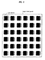
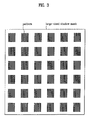
FIG. 2 , the sagging of the shadow mask becomes more greater when unit devices are mass produced on a large sized substrate, because, as shown inFIG. 3 , the size of the shadow mask is required to be large the same as the substrate, and many patterns are formed on the shadow mask. - To cope with this problem, a tension is applied to the shadow mask, which however causes deformation of the mask patterns, i.e., distortion, or elongation, that makes accuracy of the deposition process poor, to limit a size of the mask.
- Moreover, even if a shadow mask with no sagging is used, metal stripes on the mask are susceptible to vibration even by a weak impact, to give damage to the barriers of the panel. That is, since a gap between the shadow mask and the panel is very small, the vibration to the mask gives damage to the barriers at the highest positions among the barriers formed on the panel, which may cause shorts between pixels in fabrication of second electrodes.
- However, one attempt to provide a larger gap between the shadow mask and the panel for preventing the damage to the barrier results in deposition of the materials at inaccurate positions due to a shadow effect that causes another problem.
-
JP 09-120592 A - The mask comprises a mask plate which has three pins around an opening. Each of the openings of the mask plate can be provided with a mask having pin holes as well as an opening for setting up the shape of the opening in the mask plate suitably. The masks are arranged at the location of the openings in the mask plate and being adjusted by the three pins penetrating the pin holes. The pins are also used to adjust film forming substrates relative to the masks and the openings.
- Upon placing film forming substrates like plastic boards for an optical card on the masks, the mask plate is moved for closing the mask. Then the mask with the film formation substrates is moved to a film deposition system where a film on the film forming substrates is deposited by a sputtering system.
-
US 3,352,282 is concerned with a vacuum deposit device including means to register and manipulate mask and substrate elements, and discloses a substrate plate provided with a plurality of accurately spaced openings. Each of the openings is adapted to receive a substrate holder, each of which is held in place by suitable clamps. Further, a mask plate is provided with a plurality of accurately spaced openings or ports which correspond in number and in location to the openings or ports in the substrate plate. - Each of the openings of the mask plate is adapted to receive a mask when in registration with a substrate in corresponding openings that controls the pattern of deposition of material evaporized from a source. Further, the vacuum deposit device comprises a shutter plate so that only one substrate can be subjected to evaporation at the same time.
-
DE 297 07 686 U1 discloses a mask suitable to be used in the production of large sized display panels having a supporting frame onto one surface of which a film mask having openings is placed. A substrate to be treated is placed on that surface of the film mask that is opposite to the supporting frame. On the backside of the substrate a holding frame having a plurality of permanent magnets and having openings corresponding to the openings of the mask is arranged to keep the mask in tight contact with the substrate by magnetic force, so that the film mask is held exactly in parallel with the surface of the substrate to be treated. - It is an object of the present invention to provide an improved mask for fabricating large sized display panels that is prevented from sagging or shadowing.
- This object is achieved by a mask according to the present invention as defined in the appended claims.
- In particular, according to the present invention the mask for fabricating large sized display panels comprises a main frame having a plurality of holes formed therein so that each hole can accommodate one of a plurality of submasks, each having at least one pattern, wherein each of the submasks is placed in one of the holes in such a way that each submask can be individually moved in up and down, and left and right directions within the hole of the main frame for fine adjustment of each submask to align the patterns of each submask at an exact position.
- The accompanying drawings, which are included to provide a further understanding of the invention and are incorporated in and constitute a part of this specification, illustrate embodiments of the invention and together with the description serve to explain the principles of the invention:
- In the drawings:
-
FIGS. 1A and 1B illustrate a strip type, and a delta type shadow masks, respectively; -
FIG. 2 illustrates a large sized panel for use in a mass production of unit devices; -
FIG. 3 illustrates a related art large sized shadow mask for use with the large sized panel inFIG. 2 ; -
FIG. 4 illustrates a sub-mask in accordance with a preferred embodiment of the present invention; -
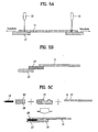
FIGS. 5A - 5C illustrate sections each showing a method for fastening a sub-mask and a sub-frame in accordance with a preferred embodiment of the present invention; -
FIG. 6 illustrates a main frame of a large sized mask the sub-mask inFIG. 4 is placed thereon; and, -
FIG. 7 illustrates a large sized mask in accordance with a preferred embodiment of the present invention. - Reference will now be made in detail to the preferred embodiments of the present invention, examples of which are illustrated in the accompanying drawings. The present invention suggests to fabricate a main frame having a plurality of holes, and fitting sub-masks in the holes respectively according to panel sizes and patterns intended to fabricate, for providing a mask suitable for fabrication of large sized, or mass production of, display panels that have neither sagging, nor shadowing.
-
FIG. 4 illustrates a sub-mask in accordance with a preferred embodiment of the present invention. - Referring to
FIG. 4 , the sub-mask in accordance with a preferred embodiment of the present invention includes asub-mask 11 having at least one pattern, and asub-frame 12 fixed to edges around thesub-mask 11 for fastening the sub-frame. Thesub-mask 11 may have a pattern formed thereon varied as a designer desires, or a plurality of patterns, within a limit the patterns cause no sagging of thesub-mask 11. - The
sub-frame 12 fixed around thesub-mask 11 may be formed of metal, polymer, inorganic material, or the like, which is formable, and strong against bending, such as aluminum, nickel, tungsten, titanium, iron, copper, or an alloy of them in metal, or plastic in polymer, or glass, or wafer in inorganic material. - There may be a variety of methods for fixing the sub-mask to the
sub-frame 12, of which three methods as shown inFIGS. 5A-5C are used. - Referring to
FIG. 5A , in a first method, thesub-mask 11 is mounted on thesub-frame 12, tension is applied to thesub-mask 11 uniformly for preventing sagging of thesub-mask 11, and thesub-mask 11 is fixed to thesub-frame 12 by using alaser 13. - Referring to
FIG. 5B , in a second method, a piece offiber 14 like a net is attached around thesub-mask 11 with adhesive, and tension is applied to thefiber 14 for fixing to thesub-frame 12. Thefiber 14 is attached to thesub-mask 11 and thesub-frame 12 with adhesive. - Referring to
FIG. 5C , ajig 15 may be used. That is,holes 17 are formed in edge region of thesub-mask 11,lateral holes 18 passed through sides of thesub-frame 12 are formed, thesub-mask 11 is fastened to thejig 15 by using theholes 17, and thesub-frame 12 is fastened to thejig 15 withscrews 16, to fix thesub-mask 11 to thesub-frame 12. - Referring to
FIG. 6 , when the sub-mask fabricated thus is mounted on themain frame 21, a mask for fabricating a large display panel can be fabricated. In this instance, thesub-mask 11 is fitted to every hole in themain frame 21. - A number of holes in the
main frame 21 are dependent on a number of devices to be fabricated, and the number of holes in themain frame 21 is required to be more than the number of the sub-mask 11 to be mounted on themain frame 21, because there may be a case when the sub-masks 11 are mounted only in holes at required positions according to forms of devices a designer intends to fabricate. - The
main frame 21 is fabricated to have a size equal to, or greater than a panel size a material is to be deposited thereon. The sub-mask 11 is fabricated to be movable in the hole in themain frame 21 in up and down, and left and right directions, for fine adjustment of the sub-mask 11 to align the patterns on the sub-mask 11 at an exact positions, by using MEMS (Microelectric Machine System). - Alike the
sub-frame 12, themain frame 21 may be formed of metal, polymer, or inorganic material, or the like, which are formable and strong against bending, such as aluminum, tungsten, titanium, iron, copper, or an alloy of them as the metal, plastic as the polymer, or glass or wafer as the inorganic material. - Referring to
FIG. 7 , upon mounting the sub-masks 11 on themain frame 21 by the foregoing methods, fabrication of a large sized mask is completed. According to this, since the large sized mask of the present invention is supported on thesub-frame 12 partly, and on themain frame 21 wholly, the large sized mask is not involved in sagging, or shadowing like the related art. Moreover, since the large sized mask of the present invention permits individual mounting/dismounting of the sub-masks 11 to/from the holes in themain frame 21, fabrication of devices according to intention of the designer and fabrication of a large sized device are easy, and mass production is favorable. - As one embodiment, the steps of a process for fabricating an organic EL display panel by using the mask of the present invention will be explained.
- At first, a large sized transparent substrate is provided, first electrode stripes, first electrode pads, and second electrode pads are formed on the substrate, and barriers are formed between luminescent regions perpendicular to the first electrodes. Then, a large sized mask of the present invention is placed on the substrate, and fine adjustment of positions of the sub-masks is made for accurate alignment of the patterns on the sub-mask with the luminescent regions on the substrate. A red luminescent layer is deposited on a red luminescent region of the substrate, and the large sized mask is moved. A green luminescent layer is deposited on a green luminescent region of the substrate, and the large sized mask is moved, again. Then, a blue luminescent layer is deposited on a blue luminescent region of the substrate. Next, a second electrode material is deposited on an entire surface of the substrate, to form the second electrode stripes in the luminescent region. Finally, a protection film is formed on the second electrode, encapsulation is conducted, to complete fabrication of the organic EL display panel.
- Thus, because the mask for fabricating a display panel of the present invention is not involved in sagging, or shadowing, the mask of the present invention can improve a fabrication accuracy, and reliability, and is suitable for fabrication of large sized panel, or mass production, thereby dropping a fabrication cost. Moreover, the possibility of mounting/dismounting of mask makes maintenance of the mask easy.
- It will be apparent to those skilled in the art that various modifications and variations can be made in the mask for fabricating a display panel of the present invention without departing the invention. Thus, it is intended that the present invention cover the modifications and variations of this invention provided they come within the scope of the appended claims.
Claims (8)
- A mask for fabricating a large sized display panel, characterized in that:- a plurality of sub-masks (11) each having at least one pattern; and- a main frame (21) having a plurality of holes formed therein for supporting the sub-masks (11) are provided,- wherein each of the sub-masks (11) is placed in one relevant hole of the holes, and is individually movable in up and down, and left and right directions within the relevant hole of the main frame for fine adjustment.
- A mask as claimed in claim 1, wherein the sub-mask (11) has four sides fixed to a sub-frame (12).
- A mask as claimed in claim 2, wherein the fixation between the sub-frame (12) and the sub-mask (11) is made by laser, adhesive, or a connecting device.
- A mask as claimed in claim 2, wherein the sub-frame (12), and the main frame (21) are formed of metal, polymer, or an inorganic material.
- A mask as claimed in claim 4, wherein the metal is aluminum, nickel, tungsten, titanium, iron, copper, or an alloy of them, the polymer is plastic, and the inorganic material is glass, or wafer.
- A mask as claimed in one of the preceding claims, wherein a number of the holes in the main frame (21) is equal to, or greater than a number of the sub-masks (11).
- A mask as claimed in one of the preceding claims, wherein the number of the holes formed in the main frame (21) is depending on a number of devices intended to fabricate.
- A mask as claimed in one of the preceding claims, wherein a size of the main frame (21) is equal to, or greater than a panel on which a material is to be deposited.
Applications Claiming Priority (2)
| Application Number | Priority Date | Filing Date | Title |
|---|---|---|---|
| KR10-2000-0071327A KR100382491B1 (en) | 2000-11-28 | 2000-11-28 | shadow mask in organic electroluminescence |
| KR2000071327 | 2000-11-28 |
Publications (3)
| Publication Number | Publication Date |
|---|---|
| EP1209522A2 EP1209522A2 (en) | 2002-05-29 |
| EP1209522A3 EP1209522A3 (en) | 2004-09-29 |
| EP1209522B1 true EP1209522B1 (en) | 2010-06-16 |
Family
ID=19702008
Family Applications (1)
| Application Number | Title | Priority Date | Filing Date |
|---|---|---|---|
| EP01128145A Expired - Lifetime EP1209522B1 (en) | 2000-11-28 | 2001-11-27 | Mask for fabricating display panel |
Country Status (6)
| Country | Link |
|---|---|
| US (1) | US6866720B2 (en) |
| EP (1) | EP1209522B1 (en) |
| JP (1) | JP2002221912A (en) |
| KR (1) | KR100382491B1 (en) |
| CN (1) | CN1209681C (en) |
| DE (1) | DE60142385D1 (en) |
Families Citing this family (56)
| Publication number | Priority date | Publication date | Assignee | Title |
|---|---|---|---|---|
| DE60228599D1 (en) * | 2001-08-24 | 2008-10-09 | Dainippon Printing Co Ltd | MASKING DEVICE FOR FORMING MULTIPLE VACUUM SIDING PAGES |
| KR100490534B1 (en) * | 2001-12-05 | 2005-05-17 | 삼성에스디아이 주식회사 | Mask frame assembly for thin layer vacuum evaporation of Organic electro luminescence device |
| KR100472012B1 (en) * | 2001-12-17 | 2005-03-08 | 조수제 | Shadow mask and the method of its fabrication |
| US6821348B2 (en) * | 2002-02-14 | 2004-11-23 | 3M Innovative Properties Company | In-line deposition processes for circuit fabrication |
| US20030151118A1 (en) * | 2002-02-14 | 2003-08-14 | 3M Innovative Properties Company | Aperture masks for circuit fabrication |
| US6897164B2 (en) * | 2002-02-14 | 2005-05-24 | 3M Innovative Properties Company | Aperture masks for circuit fabrication |
| US6727125B2 (en) * | 2002-04-17 | 2004-04-27 | Sharp Laboratories Of America, Inc. | Multi-pattern shadow mask system and method for laser annealing |
| KR100813832B1 (en) * | 2002-05-31 | 2008-03-17 | 삼성에스디아이 주식회사 | Evaporation mask frame assembly and manufacturing method thereof |
| CN100464440C (en) * | 2002-06-03 | 2009-02-25 | 三星移动显示器株式会社 | Mask frame assembly for thin layer vacuum evaporation of organic electroluminescent devices |
| US20030221620A1 (en) * | 2002-06-03 | 2003-12-04 | Semiconductor Energy Laboratory Co., Ltd. | Vapor deposition device |
| KR100480705B1 (en) * | 2002-07-03 | 2005-04-06 | 엘지전자 주식회사 | shadow mask for fabricating organic electroluminescence device and fabrication method of the same |
| KR100499476B1 (en) * | 2002-07-22 | 2005-07-05 | 엘지전자 주식회사 | shadow mask in organic electroluminescence device |
| US6729927B2 (en) * | 2002-08-01 | 2004-05-04 | Eastman Kodak Company | Method and apparatus for making a shadow mask array |
| KR100698044B1 (en) * | 2002-10-19 | 2007-03-23 | 엘지.필립스 엘시디 주식회사 | Mask design method and panel formation method |
| KR100463532B1 (en) * | 2002-10-22 | 2004-12-29 | 엘지전자 주식회사 | fabrication method for display panel using large scale full-color |
| US6926840B2 (en) * | 2002-12-31 | 2005-08-09 | Eastman Kodak Company | Flexible frame for mounting a deposition mask |
| JP4089632B2 (en) * | 2003-03-07 | 2008-05-28 | セイコーエプソン株式会社 | Mask manufacturing method, mask manufacturing apparatus, and film forming method of light emitting material |
| KR100534580B1 (en) * | 2003-03-27 | 2005-12-07 | 삼성에스디아이 주식회사 | Deposition mask for display device and Method for fabricating the same |
| JP2005276480A (en) * | 2004-03-23 | 2005-10-06 | Seiko Epson Corp | Mask, mask manufacturing method, thin film pattern forming method, electro-optical device manufacturing method, and electronic apparatus |
| KR100659057B1 (en) | 2004-07-15 | 2006-12-21 | 삼성에스디아이 주식회사 | Thin film deposition mask frame assembly and organic light emitting display device |
| KR100676177B1 (en) * | 2005-03-22 | 2007-02-01 | 엘지전자 주식회사 | Device for manufacturing organic light emitting display device |
| KR100662558B1 (en) * | 2005-12-13 | 2006-12-28 | 삼성전자주식회사 | Mask and manufacturing method of display device using same |
| WO2007099518A1 (en) * | 2006-03-03 | 2007-09-07 | Ecole Polytechnique Federale De Lausanne (Epfl) | Stencil mask for accurate pattern replication |
| KR100775846B1 (en) * | 2006-09-04 | 2007-11-13 | 엘지전자 주식회사 | Display device manufacturing mask |
| KR100853544B1 (en) * | 2007-04-05 | 2008-08-21 | 삼성에스디아이 주식회사 | Mask frame assembly for thin film deposition on flat panel display and deposition equipment using the same |
| KR100947442B1 (en) * | 2007-11-20 | 2010-03-12 | 삼성모바일디스플레이주식회사 | Vertical deposition mask manufacturing apparatus and manufacturing method of vertical deposition mask using same |
| TWI398533B (en) * | 2009-12-29 | 2013-06-11 | Au Optronics Corp | Shadow mask and method of making the same |
| KR101182440B1 (en) * | 2010-01-11 | 2012-09-12 | 삼성디스플레이 주식회사 | Mask frame assembly for thin film deposition |
| CN102110787B (en) * | 2010-11-05 | 2012-07-25 | 四川虹视显示技术有限公司 | OLED mask plate alignment method |
| KR101759347B1 (en) * | 2010-12-14 | 2017-08-01 | 삼성디스플레이 주식회사 | Mask frame assembly for thin film deposition and the manufacturing method thereof |
| KR101693578B1 (en) * | 2011-03-24 | 2017-01-10 | 삼성디스플레이 주식회사 | Vapor deposition mask |
| JP5890252B2 (en) * | 2012-05-30 | 2016-03-22 | 日本航空電子工業株式会社 | Electrical connector |
| US9583364B2 (en) | 2012-12-31 | 2017-02-28 | Sunedison Semiconductor Limited (Uen201334164H) | Processes and apparatus for preparing heterostructures with reduced strain by radial compression |
| KR20140109699A (en) * | 2013-03-06 | 2014-09-16 | 삼성디스플레이 주식회사 | Mask structure and Mask assembly including the same and Method of manufacturing the mask structure |
| KR20140125191A (en) * | 2013-04-18 | 2014-10-28 | 삼성디스플레이 주식회사 | Deposition apparatus |
| CN103235451A (en) * | 2013-04-23 | 2013-08-07 | 北京京东方光电科技有限公司 | Mask and production method thereof |
| GB201311738D0 (en) * | 2013-06-29 | 2013-08-14 | British Telecomm | Apparatus |
| CN103757589A (en) * | 2014-01-23 | 2014-04-30 | 上海和辉光电有限公司 | Masking device, system and method for manufacturing the masking device |
| US10745796B2 (en) * | 2014-10-17 | 2020-08-18 | Advantech Global, Ltd | Multi-mask alignment system and method |
| WO2016061215A1 (en) * | 2014-10-17 | 2016-04-21 | Advantech Global, Ltd | Multi-mask alignment system and method |
| CN105986225A (en) * | 2015-02-16 | 2016-10-05 | 上海和辉光电有限公司 | Shielding layer for OLED evaporation and manufacturing method thereof |
| KR102404575B1 (en) * | 2015-10-12 | 2022-06-03 | 삼성디스플레이 주식회사 | Deposition apparatus and manufacturing method of organic light emittion dioed display using the same |
| CN105568217B (en) * | 2016-01-06 | 2017-12-05 | 京东方科技集团股份有限公司 | Metal mask plate and preparation method thereof |
| CN106527041B (en) | 2016-10-10 | 2018-10-09 | 南京中电熊猫液晶显示科技有限公司 | Mask plate and its exposure method and liquid crystal display panel |
| CN110767689B (en) * | 2018-10-31 | 2022-08-16 | 云谷(固安)科技有限公司 | Mask plate, display panel, preparation method of mask plate and display panel and display terminal |
| KR102837467B1 (en) | 2019-02-06 | 2025-07-24 | 다이니폰 인사츠 가부시키가이샤 | Deposition mask device, mask support mechanism, and manufacturing method of deposition mask device |
| CN109750257B (en) * | 2019-03-26 | 2021-03-26 | 京东方科技集团股份有限公司 | Mask plate and manufacturing method thereof |
| KR101999360B1 (en) * | 2019-05-14 | 2019-07-11 | 주식회사 핌스 | Composite frame elenent for mask assembly for thin film deposition and method for manufacturing thereof |
| CN111020477B (en) * | 2019-11-29 | 2021-12-21 | 武汉天马微电子有限公司 | Mask device, evaporation method and display panel |
| KR20210091382A (en) * | 2020-01-13 | 2021-07-22 | 삼성디스플레이 주식회사 | Mask, method of manufacturing the same, and method of manufacturing display panel |
| KR102929156B1 (en) | 2020-08-31 | 2026-02-24 | 삼성디스플레이 주식회사 | Mask, method of manufacturing the same, and method of manufacturing display panel |
| KR20220034993A (en) * | 2020-09-11 | 2022-03-21 | 삼성디스플레이 주식회사 | Deposition apparatus and method for seating mask of deposition apparatus |
| KR102435235B1 (en) * | 2020-10-07 | 2022-08-24 | 주식회사 효산 | Producing method of mask and mask |
| US11659759B2 (en) * | 2021-01-06 | 2023-05-23 | Applied Materials, Inc. | Method of making high resolution OLED fabricated with overlapped masks |
| KR20230056129A (en) * | 2021-10-19 | 2023-04-27 | 삼성디스플레이 주식회사 | Mask, mask assembly including same, and mask manufacturing method |
| CN115747714A (en) * | 2022-11-24 | 2023-03-07 | 黄石全洋光电科技有限公司 | Net tensioning machine with separated net frame and net tensioning processing method thereof |
Family Cites Families (15)
| Publication number | Priority date | Publication date | Assignee | Title |
|---|---|---|---|---|
| US3352282A (en) * | 1965-07-23 | 1967-11-14 | Bendix Corp | Vacuum deposit device including means to register and manipulate mask and substrate elements |
| JPS60181264A (en) * | 1984-02-24 | 1985-09-14 | Konishiroku Photo Ind Co Ltd | Method and device for forming film |
| JPH09120592A (en) | 1995-10-23 | 1997-05-06 | Dainippon Printing Co Ltd | Mask for film forming apparatus and film forming substrate using the same |
| JP2815004B2 (en) * | 1996-10-30 | 1998-10-27 | 日本電気株式会社 | Display device and method of manufacturing the same |
| DE29707686U1 (en) | 1997-04-28 | 1997-06-26 | Balzers Prozess Systeme Vertriebs- und Service GmbH, 81245 München | Magnetic holder for foil masks |
| JP4016220B2 (en) * | 1997-06-10 | 2007-12-05 | ホーチキ株式会社 | Vapor deposition film forming method and vacuum vapor deposition apparatus |
| JP4058149B2 (en) * | 1997-12-01 | 2008-03-05 | キヤノンアネルバ株式会社 | Mask alignment method for vacuum deposition system |
| JP2848384B1 (en) * | 1997-12-05 | 1999-01-20 | 日本電気株式会社 | Organic EL display device and manufacturing method thereof |
| KR100282392B1 (en) * | 1998-06-12 | 2001-02-15 | 구자홍 | full-colcor Organic Electroluminescent Device and method for fabricating the same |
| JP4282798B2 (en) * | 1998-11-02 | 2009-06-24 | ローム株式会社 | EL display panel and manufacturing method thereof |
| US6146489A (en) * | 1998-11-19 | 2000-11-14 | General Electric Company | Method and apparatus for depositing scintillator material on radiation imager |
| JP3575303B2 (en) * | 1998-11-26 | 2004-10-13 | トヨタ自動車株式会社 | Thin film formation method |
| KR100595170B1 (en) * | 1999-03-17 | 2006-07-03 | 엘지전자 주식회사 | Full-color organic EL display panel and manufacturing method thereof |
| KR100606439B1 (en) * | 1999-04-08 | 2006-07-31 | 엘지.필립스 엘시디 주식회사 | Electroluminescent device manufacturing method |
| JP2001237073A (en) * | 2000-02-24 | 2001-08-31 | Tohoku Pioneer Corp | Metal mask for multiple patterning and manufacturing method thereof |
-
2000
- 2000-11-28 KR KR10-2000-0071327A patent/KR100382491B1/en not_active Expired - Lifetime
-
2001
- 2001-11-27 EP EP01128145A patent/EP1209522B1/en not_active Expired - Lifetime
- 2001-11-27 US US09/993,521 patent/US6866720B2/en not_active Expired - Lifetime
- 2001-11-27 DE DE60142385T patent/DE60142385D1/en not_active Expired - Lifetime
- 2001-11-28 JP JP2001362324A patent/JP2002221912A/en active Pending
- 2001-11-28 CN CNB011381612A patent/CN1209681C/en not_active Expired - Lifetime
Also Published As
| Publication number | Publication date |
|---|---|
| DE60142385D1 (en) | 2010-07-29 |
| JP2002221912A (en) | 2002-08-09 |
| EP1209522A2 (en) | 2002-05-29 |
| CN1362642A (en) | 2002-08-07 |
| KR100382491B1 (en) | 2003-05-09 |
| CN1209681C (en) | 2005-07-06 |
| US6866720B2 (en) | 2005-03-15 |
| KR20020041654A (en) | 2002-06-03 |
| US20020062785A1 (en) | 2002-05-30 |
| EP1209522A3 (en) | 2004-09-29 |
Similar Documents
| Publication | Publication Date | Title |
|---|---|---|
| US6866720B2 (en) | Mask for fabricating display panel | |
| JP7199889B2 (en) | Film forming apparatus, film forming method, and electronic device manufacturing method | |
| US11674215B2 (en) | Full-size mask assembly and manufacturing method thereof | |
| JP7289421B2 (en) | Substrate support device and deposition device | |
| JP4216531B2 (en) | Alignment device and organic material vapor deposition method | |
| US7396558B2 (en) | Integrated mask and method and apparatus for manufacturing organic EL device using the same | |
| JP4375232B2 (en) | Mask deposition method | |
| US20030101932A1 (en) | Tension mask assembly for use in vacuum deposition of thin film of organic electroluminescent device | |
| CN114032498A (en) | Alignment apparatus and method, film forming apparatus and method, and method for manufacturing electronic device | |
| KR20100000128A (en) | A deposition mask unit for fabrication of organic light emitting display device | |
| EP3245311A1 (en) | Holding arrangement for supporting a substrate carrier and a mask carrier during layer deposition in a processing chamber, apparatus for depositing a layer on a substrate, and method for aligning a substrate carrier supporting a substrate and a mask carrier | |
| US20060110663A1 (en) | Mask for depositing thin film of flat panel display and method of fabricating the mask | |
| TW201220490A (en) | capable of preventing the sag of the center of a frame by forming a rib in the center of the frame | |
| CN109750257A (en) | Mask plate and its manufacturing method | |
| JP7241048B2 (en) | Substrate support device and deposition device | |
| CN114981468B (en) | Mask blank and mask equipment | |
| JP2020532652A (en) | FMM processing for high resolution FMM | |
| KR102748864B1 (en) | Film forming apparatus | |
| KR20190116969A (en) | Carrier to support the substrate or mask | |
| KR100603400B1 (en) | Mask for depositing thin film in flat panel display device | |
| CN114555854A (en) | Mask for manufacturing OLED and OLED manufacturing method | |
| WO2020076020A1 (en) | Frame-integrated mask and method for manufacturing frame-integrated mask | |
| KR100446467B1 (en) | Method for manufacturing flat panel display device using supplementary mask | |
| KR20120021055A (en) | Mask frame assembly and depositingmethod using the same | |
| US20100141128A1 (en) | Organic el display |
Legal Events
| Date | Code | Title | Description |
|---|---|---|---|
| PUAI | Public reference made under article 153(3) epc to a published international application that has entered the european phase |
Free format text: ORIGINAL CODE: 0009012 |
|
| AK | Designated contracting states |
Kind code of ref document: A2 Designated state(s): AT BE CH CY DE DK ES FI FR GB GR IE IT LI LU MC NL PT SE TR |
|
| AX | Request for extension of the european patent |
Free format text: AL;LT;LV;MK;RO;SI |
|
| PUAL | Search report despatched |
Free format text: ORIGINAL CODE: 0009013 |
|
| AK | Designated contracting states |
Kind code of ref document: A3 Designated state(s): AT BE CH CY DE DK ES FI FR GB GR IE IT LI LU MC NL PT SE TR |
|
| AX | Request for extension of the european patent |
Extension state: AL LT LV MK RO SI |
|
| RIC1 | Information provided on ipc code assigned before grant |
Ipc: 7G 03F 1/14 A Ipc: 7C 23C 14/04 B |
|
| 17P | Request for examination filed |
Effective date: 20050302 |
|
| AKX | Designation fees paid |
Designated state(s): DE FR GB NL |
|
| 17Q | First examination report despatched |
Effective date: 20070503 |
|
| RAP1 | Party data changed (applicant data changed or rights of an application transferred) |
Owner name: LG DISPLAY CO., LTD. |
|
| GRAP | Despatch of communication of intention to grant a patent |
Free format text: ORIGINAL CODE: EPIDOSNIGR1 |
|
| GRAS | Grant fee paid |
Free format text: ORIGINAL CODE: EPIDOSNIGR3 |
|
| GRAA | (expected) grant |
Free format text: ORIGINAL CODE: 0009210 |
|
| AK | Designated contracting states |
Kind code of ref document: B1 Designated state(s): DE FR GB NL |
|
| REF | Corresponds to: |
Ref document number: 60142385 Country of ref document: DE Date of ref document: 20100729 Kind code of ref document: P |
|
| REG | Reference to a national code |
Ref country code: NL Ref legal event code: VDEP Effective date: 20100616 |
|
| PG25 | Lapsed in a contracting state [announced via postgrant information from national office to epo] |
Ref country code: NL Free format text: LAPSE BECAUSE OF FAILURE TO SUBMIT A TRANSLATION OF THE DESCRIPTION OR TO PAY THE FEE WITHIN THE PRESCRIBED TIME-LIMIT Effective date: 20100616 |
|
| PLBE | No opposition filed within time limit |
Free format text: ORIGINAL CODE: 0009261 |
|
| STAA | Information on the status of an ep patent application or granted ep patent |
Free format text: STATUS: NO OPPOSITION FILED WITHIN TIME LIMIT |
|
| 26N | No opposition filed |
Effective date: 20110317 |
|
| REG | Reference to a national code |
Ref country code: DE Ref legal event code: R097 Ref document number: 60142385 Country of ref document: DE Effective date: 20110316 |
|
| REG | Reference to a national code |
Ref country code: FR Ref legal event code: PLFP Year of fee payment: 16 |
|
| REG | Reference to a national code |
Ref country code: FR Ref legal event code: PLFP Year of fee payment: 17 |
|
| REG | Reference to a national code |
Ref country code: FR Ref legal event code: PLFP Year of fee payment: 18 |
|
| PGFP | Annual fee paid to national office [announced via postgrant information from national office to epo] |
Ref country code: FR Payment date: 20200923 Year of fee payment: 20 Ref country code: GB Payment date: 20200923 Year of fee payment: 20 |
|
| PGFP | Annual fee paid to national office [announced via postgrant information from national office to epo] |
Ref country code: DE Payment date: 20200921 Year of fee payment: 20 |
|
| REG | Reference to a national code |
Ref country code: DE Ref legal event code: R071 Ref document number: 60142385 Country of ref document: DE |
|
| REG | Reference to a national code |
Ref country code: GB Ref legal event code: PE20 Expiry date: 20211126 |
|
| PG25 | Lapsed in a contracting state [announced via postgrant information from national office to epo] |
Ref country code: GB Free format text: LAPSE BECAUSE OF EXPIRATION OF PROTECTION Effective date: 20211126 |