EP1205065B1 - Method and apparatus for providing a clock signal with high frequency accuracy - Google Patents
Method and apparatus for providing a clock signal with high frequency accuracy Download PDFInfo
- Publication number
- EP1205065B1 EP1205065B1 EP00952618A EP00952618A EP1205065B1 EP 1205065 B1 EP1205065 B1 EP 1205065B1 EP 00952618 A EP00952618 A EP 00952618A EP 00952618 A EP00952618 A EP 00952618A EP 1205065 B1 EP1205065 B1 EP 1205065B1
- Authority
- EP
- European Patent Office
- Prior art keywords
- signal
- control
- clock signal
- incoming
- clock
- Prior art date
- Legal status (The legal status is an assumption and is not a legal conclusion. Google has not performed a legal analysis and makes no representation as to the accuracy of the status listed.)
- Expired - Lifetime
Links
Images
Classifications
-
- H—ELECTRICITY
- H04—ELECTRIC COMMUNICATION TECHNIQUE
- H04N—PICTORIAL COMMUNICATION, e.g. TELEVISION
- H04N5/00—Details of television systems
- H04N5/44—Receiver circuitry for the reception of television signals according to analogue transmission standards
- H04N5/445—Receiver circuitry for the reception of television signals according to analogue transmission standards for displaying additional information
- H04N5/44504—Circuit details of the additional information generator, e.g. details of the character or graphics signal generator, overlay mixing circuits
-
- G—PHYSICS
- G09—EDUCATION; CRYPTOGRAPHY; DISPLAY; ADVERTISING; SEALS
- G09G—ARRANGEMENTS OR CIRCUITS FOR CONTROL OF INDICATING DEVICES USING STATIC MEANS TO PRESENT VARIABLE INFORMATION
- G09G5/00—Control arrangements or circuits for visual indicators common to cathode-ray tube indicators and other visual indicators
- G09G5/18—Timing circuits for raster scan displays
-
- H—ELECTRICITY
- H03—ELECTRONIC CIRCUITRY
- H03L—AUTOMATIC CONTROL, STARTING, SYNCHRONISATION OR STABILISATION OF GENERATORS OF ELECTRONIC OSCILLATIONS OR PULSES
- H03L7/00—Automatic control of frequency or phase; Synchronisation
- H03L7/06—Automatic control of frequency or phase; Synchronisation using a reference signal applied to a frequency- or phase-locked loop
- H03L7/08—Details of the phase-locked loop
- H03L7/14—Details of the phase-locked loop for assuring constant frequency when supply or correction voltages fail
- H03L7/146—Details of the phase-locked loop for assuring constant frequency when supply or correction voltages fail by using digital means for generating the oscillator control signal
-
- H—ELECTRICITY
- H04—ELECTRIC COMMUNICATION TECHNIQUE
- H04N—PICTORIAL COMMUNICATION, e.g. TELEVISION
- H04N5/00—Details of television systems
- H04N5/04—Synchronising
- H04N5/12—Devices in which the synchronising signals are only operative if a phase difference occurs between synchronising and synchronised scanning devices, e.g. flywheel synchronising
- H04N5/126—Devices in which the synchronising signals are only operative if a phase difference occurs between synchronising and synchronised scanning devices, e.g. flywheel synchronising whereby the synchronisation signal indirectly commands a frequency generator
Definitions
- the present invention relates to the field of video equipment and visual displays. More particularly, the present invention relates to on-screen displays generated by video equipment, such as set-top terminals and video cassette recorders, in the absence of an incoming video signal.
- a set-top terminal is a box of electronic circuitry connected between a user's television and a cable or satellite television system for assisting the user in accessing that system.
- OSDs on-screen displays
- the equipment being programmed takes temporary control of the television set or monitor to which it is connected in order to display menus, user prompts or echoes of user input to assist the user in properly programming the equipment or accessing equipment features.
- Mikado (USP 4,122,488), Barnes et al. (USP 4,631,588) and Huizer (USP 5,612,981) show that to generate a visual display on a display device, such as a television set or monitor, the information for the images to be displayed must be provided as a video signal. This is also true of an on-screen display which is derived from a video signal generated by the video equipment. Conversion of a video signal into a visual image on a display screen requires the use of a clock signal with a highly accurate frequency. For example, the generation of images on a video display device, e.g., a television set or monitor, may require a clock signal accurate to within 3 to 50 ppm. Some televisions require higher clocking accuracy than others. The first manifestation of an inaccurate clock signal is loss of color, i.e., the displayed image degrades to black and white.
- the required clock signal is inherently a part of an analog television signal and is always included as part of a digital television signal. Therefore, when a piece of video equipment takes control of a display device, e.g. a television set, and overrides an incoming video signal to provide an on-screen display, the necessary clock signal with a sufficiently accurate frequency can be derived or borrowed from the incoming video signal.
- a display device e.g. a television set
- the necessary clock signal with a sufficiently accurate frequency can be derived or borrowed from the incoming video signal.
- video equipment e.g. a set-top terminal
- video equipment e.g. a set-top terminal
- its own clock signal to support an on-screen display.
- generating a high-quality on-screen display requires a precise clock signal with a highly accurate frequency that is used to construct images from the video signal carrying the information for the on-screen display. Generating such a clock signal can be difficult.
- VCXO voltage controlled crystal oscillator
- control voltage applied to the VCXO is measured and recorded when a video signal is being received and properly displayed. Then, if the video equipment needs to generate a video signal for an on-screen display when no incoming video signal is being received, the recorded voltage value is retrieved from memory, and a corresponding voltage is applied to the VCXO to generate the required clock signal for supporting the on-screen display.
- an additional A/D converter (1 bit pwm and comparator) is used to measure the VCXO control voltage when the VCXO is locked to the timing of the incoming video signal. This control voltage is then used to adjust the control voltage of the VXCO to the same value when no video signal is being input to the equipment.
- the present invention provides a clock circuit for outputting a clock signal for video reconstruction in the absence of an incoming video signal as defined in claim 1.
- the present invention also encompasses a corresponding method of producing a clock signal for video reconstruction in the absence of an incoming video signal as defined in claim 5.
- the present invention as defined in the claims encompasses an embodiment comprising: a voltage controlled oscillator for outputting a clock signal and a control logic circuit for outputting a control signal to control the voltage controlled oscillator.
- the control logic circuit compares the clock signal with a reference clock signal, when present, and adjusts the control signal in accordance with the comparison.
- the clock signal is not necessarily the same frequency as the reference clock signal. Moreover, the clock signal being adjusted does not interfere with the display of a video signal using its own clock signal component.
- the reference clock signal is taken from an in-band or out-of-band digital data recovered clock.
- a recording circuit records the control data of the control signal during the comparison.
- the recorded control data is then used by the clock circuit to control the voltage controlled oscillator in the absence of an incoming video signal.
- US-A-4122488 discloses a synchronizing signal generator for deriving synchronizing signals in dependence on a video signal, suitable for use in a television transmitter of a television broadcast station or a domestic television receiver.
- This signal generator is adapted to maintain output of the synchronizing signal when the synchronizing signals in the input video signal include noise or disappear.
- the frequency of an oscillator is controlled by a signal output from a switching circuit.
- the control signal is derived from the incoming synchronizing signal and, at the same time, the control signal is sampled via an A/D convertor and stored.
- the switching circuit switches so that the control signal is obtained from the previously sampled data, which is input directly to the oscillator.
- US-A-4631588 discloses an apparatus for the generation and simultaneous display of computer graphics and video. In the absence of a video signal, a set DC voltage is applied to a pixel clock voltage controlled oscillator. This set DC voltage is not derived from a previous voltage when the video is present, having a fixed value of 2.5 volts.
- US-A-5612981 relates to apparatus and methods for improving timing recovery for a system clock, such as in the decoding of digital video signals, but does not address the problem of providing an accurate clock signal when no video signal is present.
- the present invention provides a device and method whereby the control information for controlling a voltage controlled oscillator ("VCXO") to produce a clock signal required for video reconstruction, when locked to the timing of an incoming video signal, is recorded. Then, in the absence of an incoming video signal, the recorded control information is retrieved to control the VCXO to produce the needed clock signal. In this way, a sufficiently accurate clock signal can be provided to support an on-screen display (“OSD”) even in the absence of an incoming video signal.
- OSD on-screen display
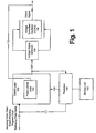
- Fig. 1 illustrates an example of a device for generating a clock signal for an on-screen display in a piece of video equipment, such as a set-top terminal, when the incoming video signal (101) is a digital signal.
- the incoming digital video signal (101) i.e. the video data stream
- the digital video signal (101) includes data fields in which a program clock reference ("PCR") is provided.
- PCR is a part of the MPEG-2 (Motion Picture Experts Group) digital signal format and functions as a digital clock signal that is used to reconstruct the images carried in the digital data stream (101) for display on a television set or monitor (not shown).
- MPEG-2 Motion Picture Experts Group
- the control logic circuit (102) using an internal phase locked loop circuit (103) will lock to the PCR data and output a corresponding control signal (107) to a voltage signal generator (104).
- the voltage signal generator (104) responds to the control signal (107) and controls the voltage controlled oscillator (VCXO) (105) to output a clock signal (106) based on the timing from the PCR.
- the clock signal (106) is fed back to the phase locked loop circuit (103) on line (112) to complete the loop.
- the circuit of Fig. 1, as described thus far, may be dedicated to providing a clock signal for on-screen display only.
- the clock signal (106) is not used in the actual reconstruction of the images from the video data stream (101).
- another circuit similar or identical to that of Fig. 1, as described thus far, would be provided for generating the clock signal used in the actual reconstruction of the images from the video data stream (101).
- the VCXO (105) illustrated in Fig. 1 may be used for producing a clock signal (106) which is used for both supporting an on-screen display and for processing the video data stream (101) for actual display.
- a processor (108) which may be part of, or separate from, the control logic circuit (102) monitors the control signal (107) output to the voltage signal generator (104).
- the processor (108) records the control data from the control signal (107).
- a memory unit (110) may be provided in which the processor (108) stores this information.
- the processor (108) can retrieve the control data from the memory unit (110) and provide the control data (109) to the control logic circuit (102).
- the control logic circuit (102) then generates a control signal (107) equivalent to that represented by the recorded control data (109) from which the voltage signal generator (104) can control the VCXO (105) to produce an appropriate clock signal.
- the processor (108) may also monitor the presence or absence of the incoming data stream (101) over line (111) so as to automatically provide the control data (109) when the incoming data stream (101) is absent. In this way, an appropriate clock signal for an on-screen display can be provided automatically in the absence of an incoming video data stream.
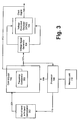
- Other means of noting the absence of the incoming video signal and initiating retrieval of the control data stored in memory are also within the scope of the present invention as described below with reference to Fig. 3.
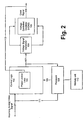
- Fig. 2 illustrates an example for working with an incoming analog video signal (201).
- the timing for reconstructing video data from the analog video signal is indicated by the horizontal frequency of the analog video signal. Consequently, the control logic circuit (102) uses its phase locked loop (103, 112) to lock to the horizontal frequency of the analog video signal (201).
- control logic circuit (102) Based on this phase lock, the control logic circuit (102) outputs a corresponding control signal (107) which drives the voltage signal generator (104) causing the VXCO (105) to output a clock signal (106) that corresponds to the timing data from the horizontal frequency of the analog video signal (201). As before, this clock signal (106) may or may not be used in the actual reconstruction of video images from the analog video signal (201).
- the processor (108) will monitor the control signal (107) and record the control data represented thereby, preferably in the memory unit (110) when the phase locked loop (103) is locked to the horizontal frequency of the incoming analog signal (201). In the absence of the analog signal (201), the processor (108) provides a signal (109) to the control logic conveying the recorded control data so that an equivalent control signal (107) can be generated and output to the voltage signal generator (104). The generator (104) then drives the VCXO to produce an appropriate clock signal for use in supporting an on-screen display even in the absence of an incoming video signal (201).
- a demodulator (302) is used to provide a clock signal (301) based on the out-of-band or in-band digital data recovered clock.
- This clock signal (301) does not necessarily or even likely have the frequency needed for a clock signal (106).
- the out-of-band reference clock signal has a frequency of 2.048 MHz. While the frequency desired for clock signal (106) to support an on-screen display is 27 MHz. However, the reference clock signal (301) can still be used as a basis to generate a control signal (107) that will result in a clock signal (106) with the appropriate frequency.
- the clock signal (301) is fed to the control logic circuit (102) which outputs the control signal (107) for the voltage signal generator (104) based thereon.
- the voltage signal generator (105) then outputs a clock signal (106).
- the processor (108) may ensure the validity of the reference clock signal (301) over line (111) by monitoring the lock status of the demodulator (302).
- the clock signal (106) is fed back to a frequency comparator (303) in the control logic circuit (102) over feed back line (112).
- the frequency comparator (303) will compare the frequency of the resulting clock signal (106) to that of the reference clock signal (301).
- clock signal (106) has a different frequency than that of the reference clock signal (301). Therefore, the comparator (303) adjusts for the difference and then compares the accuracy of the clock signal (106) against that of the reference clock signal (301).
- the control logic (102) will adjust the control signal (107) appropriately if the clock signal (106) is not sufficiently accurate as compared to the reference clock signal (301).
- the processor (108) When the voltage control oscillator (105) is outputting a stable clock signal (106) which is based on the reference clock signal (301) and achieving sufficient accuracy, the processor (108) will obtain and record the control data from the control signal (107). Again, the memory unit (110) may be used to store this information.
- the processor (108) can retrieve the control data from the memory unit (110) and provide the control data (109) to the control logic circuit (102).
- the control logic circuit (102) then generates a control signal (107) equivalent to that represented by the recorded control data (109) from which the voltage signal generator (104) can control the VCXO (105) to produce an appropriate clock signal.
- the processor (108) also monitors the presence or absence of an incoming video signal so as to automatically provide the control data (109) when an incoming video signal is absent. In this way, an appropriate clock signal for an on-screen display can be provided automatically in the absence of an incoming video signal.
Landscapes
- Engineering & Computer Science (AREA)
- Multimedia (AREA)
- Signal Processing (AREA)
- Physics & Mathematics (AREA)
- Computer Hardware Design (AREA)
- General Physics & Mathematics (AREA)
- Theoretical Computer Science (AREA)
- Computer Graphics (AREA)
- Television Signal Processing For Recording (AREA)
- Synchronizing For Television (AREA)
- Stabilization Of Oscillater, Synchronisation, Frequency Synthesizers (AREA)
- Signal Processing For Digital Recording And Reproducing (AREA)
Abstract
Description
Claims (8)
- A clock circuit for outputting a clock signal (106) for video reconstruction in the absence of an incoming video signal, comprising:wherein said demodulator (302) is an out-of-band demodulator, said out-of-band demodulator (302) in accordance with an out-of-band digital data recovered clock, or said demodulator (302) is an in-band demodulator, said reference clock signal (301) being output by said in-band demodulator (302) in accordance with an in-band digital data recovered clock.a voltage controlled oscillator (105) for outputting said clock signal (106);a control logic circuit (102) for outputting a control signal (107) to control said voltage controlled oscillator (105), wherein said control logic circuit (102) compares said clock signal (106) with a reference clock signal (301) and adjusts said control signal (107) in accordance with said comparison; anda circuit (108,110) comprising a processor (108) and a memory unit (110) for recording control data (109) of said control signal (107) during said comparison; whereinsaid recorded control data (109) is used by said clock circuit to control said voltage controlled oscillator (105) to generate an on-screen display in the absence of said incoming video signal; and whereinsaid processor (108) is adapted for monitoring the presence or absence of said incoming signal, for storing said control data that represents said control signal (107) in said memory unit (110) when said incoming signal is present, and for retrieving said control data from said memory unit (110) when said incoming signal is absent, said control data retrieved from said memory unit (110) being provided to said control logic circuit (102) to generate said control signal (107) when said incoming signal is absent;said control logic circuit (102) using said incoming signal to generate said control signal (107) when said incoming signal is present, and using said control data retrieved from said memory unit (110) to generate said control signal (107) when said incoming signal is absent, said control logic circuit (102) providing said control signal (107) to a voltage signal generator (104) and to said processor (108);said voltage signal generator (104) receives said control signal (107) from said control logic circuit (102) and controls said voltage controlled oscillator (105) in accordance with said control signal (107);said voltage controlled oscillator (105) outputs said clock signal (106); and whereina demodulator (302) generates said reference clock signal (301) and said processor (108) monitors said demodulator (302),
- The clock circuit of claim 1, wherein said control means (102) uses a frequency comparator (303) to generate said control signal (107).
- The clock circuit of claim 1, wherein said reference clock signal (301) has a different frequency than said clock signal (106).
- The clock circuit of claim 1, wherein the clock signal (106) output by said voltage controlled oscillator (105) has a sufficiently accurate frequency for supporting an on-screen display in the absence of said incoming signal.
- A method of generating a clock signal (106) for video reconstruction in the absence of an incoming video signal, the method comprising:using a voltage controlled oscillator (105) to generate said clock signal, said voltage controlled oscillator being controlled by a control signal output from a control logic circuit (102);monitoring the presence or absence of said incoming signal;storing control data that represents said control signal (107) in a memory-unit (110) when said incoming signal is present, said stored control data having been taken from said control signal (107) output from said control logic circuit (102) while said control logic circuit (102) compared said clock signal (106) from said voltage controlled oscillator (105) with a reference clock signal (301) and output said control signal in accordance with said comparison;retrieving said control data from said memory unit (110) when said incoming signal is absent, said control data retrieved from said memory unit (110) being provided to said control logic circuit (102) to generate said control signal (107) when said incoming signal is absent;using said incoming signal to generate said control signal (107) when said incoming signal is present;using said control data retrieved from said memory unit (110) to generate said control signal (107) when said incoming signal is absent;providing said control signal (107) to a voltage signal generator (104) and to a processor (108) ;outputting said clock signal (106); and whereinwherein said demodulator (302) is an out-of-band demodulator (302), said reference clock signal (301) being output by said out-of-band demodulator (302) in accordance with an out-of-band digital data recovered clock, or said demodulator (302) is an in-band demodulator (302), said reference clock signal (301) being output by said in-band demodulator (302) in accordance with an in-band digital data recovered clock.a demodulator (302) generates said reference clock signal (301), said processor (108) monitoring said demodulator (302),
- The method of claim 5, wherein said control logic circuit (102) uses a frequency comparator (303) to generate said control signal (107).
- The method of claim 5, wherein said reference clock signal (301) has a different frequency than said clock signal (106).
- The method of claim 5, wherein said voltage controlled oscillator (105) outputs a clock signal (106) having a frequency sufficient for supporting an on-screen display in the absence of said incoming video signal.
Applications Claiming Priority (3)
| Application Number | Priority Date | Filing Date | Title |
|---|---|---|---|
| US09/370,928 US6556250B1 (en) | 1999-08-10 | 1999-08-10 | Method and apparatus for providing a timing signal with high frequency accuracy in video equipment for supporting an on-screen display in the absence of a video signal |
| US370928 | 1999-08-10 | ||
| PCT/US2000/021578 WO2001011875A1 (en) | 1999-08-10 | 2000-08-08 | Method and apparatus for providing a clock signal with high frequency accuracy |
Publications (2)
| Publication Number | Publication Date |
|---|---|
| EP1205065A1 EP1205065A1 (en) | 2002-05-15 |
| EP1205065B1 true EP1205065B1 (en) | 2005-10-19 |
Family
ID=23461772
Family Applications (1)
| Application Number | Title | Priority Date | Filing Date |
|---|---|---|---|
| EP00952618A Expired - Lifetime EP1205065B1 (en) | 1999-08-10 | 2000-08-08 | Method and apparatus for providing a clock signal with high frequency accuracy |
Country Status (8)
| Country | Link |
|---|---|
| US (1) | US6556250B1 (en) |
| EP (1) | EP1205065B1 (en) |
| CN (1) | CN1199442C (en) |
| AT (1) | ATE307459T1 (en) |
| AU (1) | AU6528300A (en) |
| CA (1) | CA2391735A1 (en) |
| DE (1) | DE60023311D1 (en) |
| WO (1) | WO2001011875A1 (en) |
Families Citing this family (7)
| Publication number | Priority date | Publication date | Assignee | Title |
|---|---|---|---|---|
| JP2001127728A (en) * | 1999-10-29 | 2001-05-11 | Oki Electric Ind Co Ltd | Receiving circuit |
| US8331456B2 (en) | 2002-09-27 | 2012-12-11 | Broadcom Corporation | System and method for audio and visual synchronization |
| US7953194B2 (en) | 2002-09-27 | 2011-05-31 | Broadcom Corporation | Handling video transition errors in video on demand streams |
| CN101202616B (en) * | 2007-12-14 | 2011-12-28 | 华为技术有限公司 | Method and apparatus for controlling data processing |
| CN101557230B (en) * | 2008-04-10 | 2011-07-20 | 中芯国际集成电路制造(上海)有限公司 | System and method for self calibration of phase-locked loop |
| TWI429199B (en) | 2010-06-22 | 2014-03-01 | Phison Electronics Corp | Method and data transceiving system for generating reference clock signal |
| CN102315849B (en) * | 2010-07-01 | 2014-05-14 | 群联电子股份有限公司 | Method for generating reference clock signal and data transceiving system |
Family Cites Families (17)
| Publication number | Priority date | Publication date | Assignee | Title |
|---|---|---|---|---|
| US4122488A (en) | 1976-05-10 | 1978-10-24 | Nippon Television Industry Corporation | Sync signal generator with memorization of phase detection output |
| US4631588A (en) | 1985-02-11 | 1986-12-23 | Ncr Corporation | Apparatus and its method for the simultaneous presentation of computer generated graphics and television video signals |
| JPH0528850Y2 (en) * | 1987-02-18 | 1993-07-23 | ||
| JPH02309778A (en) * | 1989-05-24 | 1990-12-25 | Victor Co Of Japan Ltd | Clock generating circuit |
| US5459524A (en) * | 1991-11-18 | 1995-10-17 | Cooper; J. Carl | Phase modulation demodulator apparatus and method |
| DE4138543A1 (en) * | 1991-11-23 | 1993-05-27 | Philips Patentverwaltung | DIGITAL PHASE CONTROL CIRCUIT |
| US5473640A (en) | 1994-01-21 | 1995-12-05 | At&T Corp. | Phase-lock loop initialized by a calibrated oscillator-control value |
| US5612981A (en) | 1994-02-15 | 1997-03-18 | Philips Electronics North America Corporation | Apparatus and methods for improving timing recovery of a system clock |
| US5473385A (en) * | 1994-06-07 | 1995-12-05 | Tv/Com Technologies, Inc. | Clock correction in a video data decoder using video synchronization signals |
| US5502502A (en) * | 1995-03-06 | 1996-03-26 | Honeywell Inc. | PLL-based method and apparatus for generating video drive signals from various sync formats |
| KR0143115B1 (en) * | 1995-06-09 | 1998-07-15 | 김광호 | Symbol Timing Recovery Circuit and Method |
| WO1997007594A1 (en) * | 1995-08-14 | 1997-02-27 | Hitachi, Ltd. | Pll circuit and picture reproducing device |
| EP0836282B1 (en) * | 1996-10-08 | 2002-06-12 | Sony Corporation | Receiving apparatus and method and phase lock loop circuit |
| JP3331894B2 (en) * | 1997-01-30 | 2002-10-07 | ヤマハ株式会社 | PLL circuit |
| US5796392A (en) * | 1997-02-24 | 1998-08-18 | Paradise Electronics, Inc. | Method and apparatus for clock recovery in a digital display unit |
| US6310660B1 (en) * | 1998-03-18 | 2001-10-30 | Sony Corporation | Video signal dropout detector |
| US6009006A (en) * | 1998-08-07 | 1999-12-28 | Thomson Consumer Electronics, Inc. | Synchronized high voltage generator |
-
1999
- 1999-08-10 US US09/370,928 patent/US6556250B1/en not_active Expired - Lifetime
-
2000
- 2000-08-08 DE DE60023311T patent/DE60023311D1/en not_active Expired - Lifetime
- 2000-08-08 AU AU65283/00A patent/AU6528300A/en not_active Abandoned
- 2000-08-08 AT AT00952618T patent/ATE307459T1/en not_active IP Right Cessation
- 2000-08-08 CN CN00814026.XA patent/CN1199442C/en not_active Expired - Fee Related
- 2000-08-08 WO PCT/US2000/021578 patent/WO2001011875A1/en not_active Ceased
- 2000-08-08 EP EP00952618A patent/EP1205065B1/en not_active Expired - Lifetime
- 2000-08-08 CA CA002391735A patent/CA2391735A1/en not_active Abandoned
Also Published As
| Publication number | Publication date |
|---|---|
| US6556250B1 (en) | 2003-04-29 |
| EP1205065A1 (en) | 2002-05-15 |
| WO2001011875A1 (en) | 2001-02-15 |
| ATE307459T1 (en) | 2005-11-15 |
| CA2391735A1 (en) | 2001-02-15 |
| CN1199442C (en) | 2005-04-27 |
| CN1378739A (en) | 2002-11-06 |
| DE60023311D1 (en) | 2006-03-02 |
| AU6528300A (en) | 2001-03-05 |
Similar Documents
| Publication | Publication Date | Title |
|---|---|---|
| EP0691791B1 (en) | Method and apparatus for overlaying digitally generated graphics over an analog video signal | |
| US6532042B1 (en) | Clock supply device for use in digital video apparatus | |
| US6704009B2 (en) | Image display | |
| US6037994A (en) | Sync signal processing device for combined video appliance | |
| US6556250B1 (en) | Method and apparatus for providing a timing signal with high frequency accuracy in video equipment for supporting an on-screen display in the absence of a video signal | |
| KR20000023800A (en) | Scan converting device and scan converting method | |
| EP1023804B1 (en) | Integrated television processor | |
| US6674482B1 (en) | Apparatus for generating sync of digital television | |
| EP0306993A1 (en) | Burst/continuous wave converting apparatus for generating continuous wave in response to bursts | |
| US4992872A (en) | Method of synchronizing the horizontal deflection of electron beams in television receivers | |
| US5235425A (en) | Automatic tuning method and device thereof | |
| KR100220306B1 (en) | IF signal frequency measurement method and device | |
| US7450178B2 (en) | Display synchronization signal generator in digital broadcast receiver | |
| EP0584824B1 (en) | Oscillator circuit suitable for picture-in-picture system | |
| CN1723444B (en) | Methods for Using Simultaneous Sampling Designs in Fixed Rate Sampling Mode | |
| KR0162435B1 (en) | Multi-screen quaternary display device of TV receiver | |
| EP0865198B1 (en) | Method and device for arranging digitized image signals or data in orthogonal rows and columns | |
| US6829014B1 (en) | Frequency bounded oscillator for video reconstruction | |
| KR100317289B1 (en) | apparatus for correcting sync in digital TV | |
| US6940936B2 (en) | Alternate timing signal for a vestigial sideband modulator | |
| KR0123724B1 (en) | Synchronization signal generator and image signal processing device using same | |
| KR100207786B1 (en) | Sampling clock generating circuit of a video tape recorder | |
| JPH05153632A (en) | System clock generating circuit in muse decoder | |
| JPH0720809A (en) | Digital convergence correction device and image display device using the same | |
| JPH02135879A (en) | Video signal processing device |
Legal Events
| Date | Code | Title | Description |
|---|---|---|---|
| PUAI | Public reference made under article 153(3) epc to a published international application that has entered the european phase |
Free format text: ORIGINAL CODE: 0009012 |
|
| 17P | Request for examination filed |
Effective date: 20020222 |
|
| AK | Designated contracting states |
Kind code of ref document: A1 Designated state(s): AT BE CH CY DE DK ES FI FR GB GR IE IT LI LU MC NL PT |
|
| AX | Request for extension of the european patent |
Free format text: AL;LT;LV;MK;RO;SI |
|
| 17Q | First examination report despatched |
Effective date: 20020703 |
|
| GRAP | Despatch of communication of intention to grant a patent |
Free format text: ORIGINAL CODE: EPIDOSNIGR1 |
|
| GRAS | Grant fee paid |
Free format text: ORIGINAL CODE: EPIDOSNIGR3 |
|
| RBV | Designated contracting states (corrected) |
Designated state(s): AT BE CH CY DE DK ES FI FR GB GR IE IT LI LU MC NL PT SE |
|
| GRAA | (expected) grant |
Free format text: ORIGINAL CODE: 0009210 |
|
| AK | Designated contracting states |
Kind code of ref document: B1 Designated state(s): AT BE CH CY DE DK ES FI FR GB GR IE IT LI LU MC NL PT SE |
|
| PG25 | Lapsed in a contracting state [announced via postgrant information from national office to epo] |
Ref country code: IT Free format text: LAPSE BECAUSE OF FAILURE TO SUBMIT A TRANSLATION OF THE DESCRIPTION OR TO PAY THE FEE WITHIN THE PRESCRIBED TIME-LIMIT;WARNING: LAPSES OF ITALIAN PATENTS WITH EFFECTIVE DATE BEFORE 2007 MAY HAVE OCCURRED AT ANY TIME BEFORE 2007. THE CORRECT EFFECTIVE DATE MAY BE DIFFERENT FROM THE ONE RECORDED. Effective date: 20051019 Ref country code: AT Free format text: LAPSE BECAUSE OF FAILURE TO SUBMIT A TRANSLATION OF THE DESCRIPTION OR TO PAY THE FEE WITHIN THE PRESCRIBED TIME-LIMIT Effective date: 20051019 Ref country code: FI Free format text: LAPSE BECAUSE OF FAILURE TO SUBMIT A TRANSLATION OF THE DESCRIPTION OR TO PAY THE FEE WITHIN THE PRESCRIBED TIME-LIMIT Effective date: 20051019 Ref country code: BE Free format text: LAPSE BECAUSE OF FAILURE TO SUBMIT A TRANSLATION OF THE DESCRIPTION OR TO PAY THE FEE WITHIN THE PRESCRIBED TIME-LIMIT Effective date: 20051019 Ref country code: NL Free format text: LAPSE BECAUSE OF FAILURE TO SUBMIT A TRANSLATION OF THE DESCRIPTION OR TO PAY THE FEE WITHIN THE PRESCRIBED TIME-LIMIT Effective date: 20051019 Ref country code: CH Free format text: LAPSE BECAUSE OF FAILURE TO SUBMIT A TRANSLATION OF THE DESCRIPTION OR TO PAY THE FEE WITHIN THE PRESCRIBED TIME-LIMIT Effective date: 20051019 Ref country code: LI Free format text: LAPSE BECAUSE OF FAILURE TO SUBMIT A TRANSLATION OF THE DESCRIPTION OR TO PAY THE FEE WITHIN THE PRESCRIBED TIME-LIMIT Effective date: 20051019 |
|
| REG | Reference to a national code |
Ref country code: GB Ref legal event code: FG4D |
|
| REG | Reference to a national code |
Ref country code: CH Ref legal event code: EP |
|
| REG | Reference to a national code |
Ref country code: IE Ref legal event code: FG4D |
|
| PG25 | Lapsed in a contracting state [announced via postgrant information from national office to epo] |
Ref country code: DK Free format text: LAPSE BECAUSE OF FAILURE TO SUBMIT A TRANSLATION OF THE DESCRIPTION OR TO PAY THE FEE WITHIN THE PRESCRIBED TIME-LIMIT Effective date: 20060119 Ref country code: SE Free format text: LAPSE BECAUSE OF FAILURE TO SUBMIT A TRANSLATION OF THE DESCRIPTION OR TO PAY THE FEE WITHIN THE PRESCRIBED TIME-LIMIT Effective date: 20060119 Ref country code: GR Free format text: LAPSE BECAUSE OF FAILURE TO SUBMIT A TRANSLATION OF THE DESCRIPTION OR TO PAY THE FEE WITHIN THE PRESCRIBED TIME-LIMIT Effective date: 20060119 |
|
| PG25 | Lapsed in a contracting state [announced via postgrant information from national office to epo] |
Ref country code: DE Free format text: LAPSE BECAUSE OF FAILURE TO SUBMIT A TRANSLATION OF THE DESCRIPTION OR TO PAY THE FEE WITHIN THE PRESCRIBED TIME-LIMIT Effective date: 20060120 |
|
| PG25 | Lapsed in a contracting state [announced via postgrant information from national office to epo] |
Ref country code: ES Free format text: LAPSE BECAUSE OF FAILURE TO SUBMIT A TRANSLATION OF THE DESCRIPTION OR TO PAY THE FEE WITHIN THE PRESCRIBED TIME-LIMIT Effective date: 20060130 |
|
| REF | Corresponds to: |
Ref document number: 60023311 Country of ref document: DE Date of ref document: 20060302 Kind code of ref document: P |
|
| PG25 | Lapsed in a contracting state [announced via postgrant information from national office to epo] |
Ref country code: PT Free format text: LAPSE BECAUSE OF FAILURE TO SUBMIT A TRANSLATION OF THE DESCRIPTION OR TO PAY THE FEE WITHIN THE PRESCRIBED TIME-LIMIT Effective date: 20060320 |
|
| NLV1 | Nl: lapsed or annulled due to failure to fulfill the requirements of art. 29p and 29m of the patents act | ||
| REG | Reference to a national code |
Ref country code: CH Ref legal event code: PL |
|
| PG25 | Lapsed in a contracting state [announced via postgrant information from national office to epo] |
Ref country code: IE Free format text: LAPSE BECAUSE OF NON-PAYMENT OF DUE FEES Effective date: 20060808 |
|
| PLBE | No opposition filed within time limit |
Free format text: ORIGINAL CODE: 0009261 |
|
| STAA | Information on the status of an ep patent application or granted ep patent |
Free format text: STATUS: NO OPPOSITION FILED WITHIN TIME LIMIT |
|
| PG25 | Lapsed in a contracting state [announced via postgrant information from national office to epo] |
Ref country code: MC Free format text: LAPSE BECAUSE OF NON-PAYMENT OF DUE FEES Effective date: 20060831 |
|
| 26N | No opposition filed |
Effective date: 20060720 |
|
| EN | Fr: translation not filed | ||
| PG25 | Lapsed in a contracting state [announced via postgrant information from national office to epo] |
Ref country code: FR Free format text: LAPSE BECAUSE OF FAILURE TO SUBMIT A TRANSLATION OF THE DESCRIPTION OR TO PAY THE FEE WITHIN THE PRESCRIBED TIME-LIMIT Effective date: 20061208 |
|
| GBPC | Gb: european patent ceased through non-payment of renewal fee |
Effective date: 20060808 |
|
| REG | Reference to a national code |
Ref country code: IE Ref legal event code: MM4A |
|
| PG25 | Lapsed in a contracting state [announced via postgrant information from national office to epo] |
Ref country code: GB Free format text: LAPSE BECAUSE OF NON-PAYMENT OF DUE FEES Effective date: 20060808 |
|
| PG25 | Lapsed in a contracting state [announced via postgrant information from national office to epo] |
Ref country code: LU Free format text: LAPSE BECAUSE OF NON-PAYMENT OF DUE FEES Effective date: 20060808 |
|
| PG25 | Lapsed in a contracting state [announced via postgrant information from national office to epo] |
Ref country code: FR Free format text: LAPSE BECAUSE OF FAILURE TO SUBMIT A TRANSLATION OF THE DESCRIPTION OR TO PAY THE FEE WITHIN THE PRESCRIBED TIME-LIMIT Effective date: 20051019 Ref country code: CY Free format text: LAPSE BECAUSE OF FAILURE TO SUBMIT A TRANSLATION OF THE DESCRIPTION OR TO PAY THE FEE WITHIN THE PRESCRIBED TIME-LIMIT Effective date: 20051019 |