EP1199771A2 - Antenne - Google Patents
Antenne Download PDFInfo
- Publication number
- EP1199771A2 EP1199771A2 EP01122686A EP01122686A EP1199771A2 EP 1199771 A2 EP1199771 A2 EP 1199771A2 EP 01122686 A EP01122686 A EP 01122686A EP 01122686 A EP01122686 A EP 01122686A EP 1199771 A2 EP1199771 A2 EP 1199771A2
- Authority
- EP
- European Patent Office
- Prior art keywords
- circuit
- antenna
- impedance adapter
- housing
- antenna according
- Prior art date
- Legal status (The legal status is an assumption and is not a legal conclusion. Google has not performed a legal analysis and makes no representation as to the accuracy of the status listed.)
- Granted
Links
Images


Classifications
-
- H—ELECTRICITY
- H01—ELECTRIC ELEMENTS
- H01Q—ANTENNAS, i.e. RADIO AERIALS
- H01Q19/00—Combinations of primary active antenna elements and units with secondary devices, e.g. with quasi-optical devices, for giving the antenna a desired directional characteristic
- H01Q19/28—Combinations of primary active antenna elements and units with secondary devices, e.g. with quasi-optical devices, for giving the antenna a desired directional characteristic using a secondary device in the form of two or more substantially straight conductive elements
- H01Q19/30—Combinations of primary active antenna elements and units with secondary devices, e.g. with quasi-optical devices, for giving the antenna a desired directional characteristic using a secondary device in the form of two or more substantially straight conductive elements the primary active element being centre-fed and substantially straight, e.g. Yagi antenna
-
- H—ELECTRICITY
- H01—ELECTRIC ELEMENTS
- H01Q—ANTENNAS, i.e. RADIO AERIALS
- H01Q23/00—Antennas with active circuits or circuit elements integrated within them or attached to them
Definitions
- the present invention relates to an antenna, in particular for Reception of television, radio and / or data signals according to the generic term of Claim 1.
- antennas such as from the Spanish utility model No. 9002915, known.
- the currently on the The antennas on the market are for the reception of analog signals has been developed.
- Antennas with larger ones are used for digital television Antenna gain values required.
- the invention has for its object to provide an antenna that Meets the requirements of digital television.
- the invention has a number of advantages.
- the antenna is designed in such a way that an assigned one Impedance adapter circuit and an associated amplification circuit form a circuitry unit.
- the operation corresponds to the unit in the event of amplifier circuit failure, operation of the impedance adapter circuit.
- the antenna according to the invention is thus even after one Failure of the amplifier circuit can be used; corresponds to the antenna according to the invention in this operating case an antenna to which no amplifier circuit is assigned is.
- a further advantageous embodiment of the antenna is according to the invention in the Configured such that the impedance adapter circuit and the amplification circuit form a technical circuit unit and that the operation of the Unit in the case of its connection to a supply source, the operation of the impedance adapter circuit and corresponds to the amplification circuit. On the other hand corresponds to the operation of the unit if it is not connected to one Power source the operation of the impedance adapter circuit.
- the invention Antenna can thus be used even in cases where it is not at the source of the food is connected or fails.
- the feed source is formed in particular by a solar cell system.
- the ecological advantage of this solution is another advantage that the antenna can thus be operated without an external power source, which would also be connected to the amplification circuit via a feed line.
- the impedance adapter circuit and the amplification circuit are preferred on a common circuit board and in a common housing arranged, the housing being arranged directly on the antenna or is integrated into this.
- the signals are amplified without the noise figure deteriorating.
- the invention The antenna is therefore comparatively weak reception even in zones available.
- the housing consists of electrically conductive material and is connected to ground. So that the two circuits mentioned are against possible interference signals are shielded.
- This housing preferably has a connector for a direct or indirect connection to a receiver for television, radio and / or Data.
- the housing and the connector are formed in one piece.
- a dipole contains at least one fold. So that the radiation area of the Dipols increased and the antenna gain characteristic improved.
- the dipole can also be formed in more than one plane. With that the Surface area of the dipole increased without increasing the length of the dipole; Frequency tuning values of the antenna are retained.
- the dipole can also be designed with a flat profile. That allows one Extend the antenna bandwidth.
- the invention is based on a non-limiting embodiment of the antenna according to the invention and the drawings explained.
- Figure 1 shows the antenna with a scaffold, which by three support rods, one Main central rod 1 and two auxiliary rods 2 and 3 of lesser length, the each lie on one side of the central rod 1, is formed.
- the three bars are coplanar, with the auxiliary rods 2 and 3 slightly oblique and symmetrical to Divide the central rod 1.
- the three bars are made of tubular profiles, preferably aluminum.
- the Are bars 2 and 3; the three rods 1, 2, 3 are antenna at the rear end aligned with the three rods towards the rear end of the end are arranged diverging.
- the three bars 1, 2 and 3 are in one Rear radome 4 introduced.
- the central rod 1 is inserted into the rear radome 4, a support 5 being mounted on an adjoining rod section is on which the reflector 6 is attached.
- the bars 1, 2 and 3 have a number of identical bars 7 which are mounted along the structure in the direction perpendicular to the bars. These rods 7 represent the director elements of the antenna.
- the rods 1, 2 and 3 are mounted in the rear radome 4 and in the front radome 8.
- the reflector 6 consists of two panels 9 and 10, the element rods 11 exhibit.
- the panels are each in an inclined position in a support element 5 stored with respect to the central rod 1.
- the element rods 11 are on their ends are held by holding elements 12.
- the dipole 13 In the rear radome 4 are the dipole 13 and an inner housing (junction box) 14 arranged, the impedance adapter circuit 15 and the amplification circuit 16 ( Figure 5) records (Fig.4).
- the antenna is attached to a vertical mast 17 by means of an auxiliary clamp 18 free end of the central rod 1 attached.
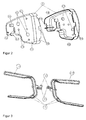
- Figure 2 shows that the rear radome 4 revolving symmetrical covers 41 and 42 has a trapezoidal shape, which has the rods 1, 2 and 3 of the antenna structure take up.
- the rods 1, 2 and 3 are in openings 45 in the front area held while the rod 1 is held in the rear region in the opening 46 becomes.
- the covers 41 and 42 are screwed into the through holes 43 grab, connected.
- These covers 41, 42 still have openings 44, which receive the rods 7, which go to the sections of the rods 1, 2 and 3 (Fig.1) belong.
- the rear radome 4 has a recess 47 in the lower region, in which the Dipole 13 and the housing 14 is seated.
- window paths 48 are provided for anchoring the support part 19 (Fig. 4) of the housing 14.
- the rear radome 4 has longitudinal opening paths 49 to insert the dipole 13.
- FIG. 3 shows in detail the dipole 13 of the antenna, which consists of two parts 131 in Composed U-shape, which have folds 134 on its broad side. This allows the radiation surface of the dipole to be enlarged, thereby improving Gain properties of the antenna can be achieved.
- the parts 131 each have a fin 132 in an L-shape at their base, wherein the base each has a folding part, in each of which an opening 133 for Connect the dipole.
- the dipole can be formed in more than one plane. With that the Surface area of the dipole increased without increasing the length of the dipole; Frequency tuning values of the antenna are retained.
- the dipole can also be designed with a flat profile, which is an expansion the antenna bandwidth allowed.
- FIG. 4 shows the housing 14, which consists of a rectangular body (base) 141 and a cover 142, the base and cover using threaded screws are closed by recesses 144 of the cover guided and inserted into openings 143 of the base.
- the base has in her Interior bolt 145 on which a circuit board with an electronic Circuit, in particular with the amplification circuit 16 and the impedance matching circuit is put on.
- the housing 14 houses the impedance adapter circuit 15 and the amplification circuit 16 on; the housing 14 is arranged directly on the antenna or integrated into this. It is made of electrically conductive material and is mass connected.
- the base 141 of the housing 14 has one in one of its side walls Plug connector (socket) 21 for a direct or indirect connection to a TV, radio and / or data signal receiver.
- the connector 21 and that Housing 4 are integrally formed. It will be a comparatively good one electrical adaptation between the receiving devices and the antenna, possible Interference signals are limited in their effect.
- the base of the housing 14 has two openings 146 through which the pins 191 are guided, which belong to the support 19 of the housing. These pins have 191 Internal openings, in which screws are arranged, the electrical connection between the dipole 13 and the amplification circuit 16, which in the Housing 14 is arranged, manufacture.
- Figure 5 shows the circuit diagram of the matching circuit 15 and the electrical Boost circuit 16.
- the matching circuit 15 is formed by the printed line J1.
- the electrical amplification circuit 16 is configured as follows. She instructs first filter, that is, a high-pass filter, which is formed by the capacitors C1, C2 and C6, the diode D3 and the coil CH2 is formed. Furthermore, it has one Amplification stage, which consists of the transistor T1 and its polarizing circuit, consisting of resistors R1, R2, R3, R4 and R6, capacitors C3 and C4, and the coils L1 and CH1 is formed. Circuit 16 also extends far an output stage consisting of the capacitors C5, C11, C8 and the coils CH3 and CH5 is formed.
- the electrical amplification circuit 16 has electrical switching paths, one Pass-through circuit and a protective circuit.
- the pass circuit is through the capacitors C7, C9 and C14 the diodes D1 and D2, the capacitance diode (Varicap) D5, the resistors R5 and R8 and formed by a printed line J2. This through circuit allows the signal to pass as soon as the amplification stage has no power supply is fed.
- the protection circuit comprises a diode D4 and a resistor R9.
- This Protection circuit leads the signal to the output, which is the through circuit (C7, C9, C14, D1, D2, D5, R5, R8, J2) passes through when the gain stage has no power supply, which avoids this signal going to the polarizing circuit of the transistor T1 is derived.
- the gain stage is connected to the output connector of the antenna (21 in Figure 4, corresponding to the galvanic connection RF_OUT + Vcc in Figure 5) fed, by means of a coaxial cable that connects the antenna to the rest Connects facilities of the system.
- the supply voltage can come from head units, which are available on the market and are already designed for this, or can be supplied via the coaxial cable.
- the gain circuit 16 is in close proximity to the impedance adapter circuit 15 arranged (no geometric distance between 16 and 15 or 0 millimeters).
- the impedance adapter circuit 15 and the amplification circuit 16 form one circuitry unit, the operation of the unit in the event of a failure the amplification circuit 16 (failure of at least one circuit component; no supply voltage) the operation of the impedance adapter circuit 15 equivalent.
- an amplifier on the antenna as described above is on is associated with the disadvantage that the amplifier influences the weather is exposed to a functional restriction or to the destruction of the Can lead amplifier. For example, rain falling into the Penetration of amplifier housing, short circuits and destruction of Effect circuit components.
- an electrical one Discharge which is an overvoltage in the amplification circuit and a Burning circuit components causes.
- the probability for this is in the amplification circuit according to FIG reduced by the protection circuit made up of capacitors C1 and C2 coil CH2 and diode D3. These are in the way designed that overvoltages are absorbed by a possible Radiation can be caused to reach the antenna.
- the components, which are comparatively at risk are semiconductor components, here the Transistor T1, diodes D1, D2, D4 and varicap diode D5.
- the failure of the Transistor T1 would lead to the failure of the amplifier circuit.
- diode D4 would cause the amplifier circuit to continue operating, but also that it is separated from the output of the circuit, which is what Result means the unavailability of the amplifier.
- the failure of the two Diodes D1 and D2 would cause the amplifier to go into one Vibration state is offset.
- the failure of the varicap diode D5 would Do not influence the operation of the amplifier. While usually the failure a circuit component of the amplifier disables the antenna and requires that the antenna or circuit be replaced is the Circuit according to the invention designed in such a way that if the Amplifier the antenna can be used as a conventional antenna; the adapter circuit remains with the output connector over the Line J2 and connected via the arrangement of C14 and diode D5. It is at Only need to deactivate the supply voltage source.
- the circuitry unit consisting of circuits 15 and 16, functions in normal operation when it is supplied with the appropriate voltage is used as an impedance matching and as a gain circuit. Thereby reduced the capacity of D5 increases when the voltage is increased on the input side. D1 and D2 become senior. This prevents a signal from being routed via J2, since C14 together with D5 form a large impedance while the residual signal is grounded via C9 and C7. Overall it is achieved that the Antenna received signal is routed through the amplifier stage. On Vibration condition is avoided. Finally, diode D4 allows if it is fed so that the signal of the amplifier is led to the output.
- the circuitry unit consisting of circuits 15 and 16, acts as if it is not supplied with the appropriate voltage Impedance matching circuit.
- the signal from J1 goes to Output namely through J2 and the arrangement of J14 and D5 which is a big one Capacity when no voltage is supplied to the unit.
- the diodes D1 and D2 prevent the signal from being derived via C9 and C7, respectively; the Diode D14 performs the same function with regard to the collector of transistor T1 and the elements CH1, R3, C4, R4, R6 and C8.
- the elements L1, R1 and C3 prevent loss of the signal through the input of the amplifier.
Applications Claiming Priority (8)
| Application Number | Priority Date | Filing Date | Title |
|---|---|---|---|
| ES200002389 | 2000-09-29 | ||
| ES200002387A ES2182658B1 (es) | 2000-09-29 | 2000-09-29 | Antena. |
| ES200002386 | 2000-09-29 | ||
| ES200002388A ES2183692B2 (es) | 2000-09-29 | 2000-09-29 | Antena. |
| ES200002389A ES2184577B1 (es) | 2000-09-29 | 2000-09-29 | Antena. |
| ES200002386A ES2182657B1 (es) | 2000-09-29 | 2000-09-29 | Antena. |
| ES200002387 | 2000-09-29 | ||
| ES200002388 | 2000-09-29 |
Publications (3)
| Publication Number | Publication Date |
|---|---|
| EP1199771A2 true EP1199771A2 (fr) | 2002-04-24 |
| EP1199771A3 EP1199771A3 (fr) | 2004-05-06 |
| EP1199771B1 EP1199771B1 (fr) | 2007-04-18 |
Family
ID=27444002
Family Applications (1)
| Application Number | Title | Priority Date | Filing Date |
|---|---|---|---|
| EP01122686A Expired - Lifetime EP1199771B1 (fr) | 2000-09-29 | 2001-09-29 | Antenne |
Country Status (7)
| Country | Link |
|---|---|
| EP (1) | EP1199771B1 (fr) |
| AT (1) | ATE360270T1 (fr) |
| CY (1) | CY1106729T1 (fr) |
| DE (1) | DE50112365D1 (fr) |
| DK (1) | DK1199771T3 (fr) |
| ES (1) | ES2287059T3 (fr) |
| PT (1) | PT1199771E (fr) |
Cited By (4)
| Publication number | Priority date | Publication date | Assignee | Title |
|---|---|---|---|---|
| DE202009002347U1 (de) | 2008-02-19 | 2009-05-20 | Televés, S.A., Santiago de Compostela | Antenne |
| EP2221966A1 (fr) | 2008-12-19 | 2010-08-25 | Televes, S.A. | Dispositif de traitement de signaux de télécommunication pour antennes |
| WO2010130163A1 (fr) * | 2009-10-19 | 2010-11-18 | Yang Kendy | Antenne extérieure |
| ITBS20110024A1 (it) * | 2011-03-01 | 2012-09-02 | Emme Esse Spa | Antenna televisiva a piu' culle |
Citations (5)
| Publication number | Priority date | Publication date | Assignee | Title |
|---|---|---|---|---|
| US3992669A (en) * | 1975-08-29 | 1976-11-16 | Gte Automatic Electric Laboratories Incorporated | Radio frequency protection circuit |
| EP0540899A1 (fr) * | 1991-10-11 | 1993-05-12 | Televes, S.A. | Antenne UHF Yagi |
| US5418490A (en) * | 1994-03-01 | 1995-05-23 | Tx Rx Systems, Inc. | Failure responsive alternate amplifier and bypass system for communications amplifier |
| DE29607742U1 (de) * | 1996-04-29 | 1996-07-25 | Wohlmeiner Dietmar | Funkbetriebenes Satellitenempfangssystem |
| WO1998043417A1 (fr) * | 1997-03-25 | 1998-10-01 | Terk Technologies Corporation | Sous-systeme de reception sans fil avec antenne et amplificateur commutable |
-
2001
- 2001-09-29 AT AT01122686T patent/ATE360270T1/de active
- 2001-09-29 EP EP01122686A patent/EP1199771B1/fr not_active Expired - Lifetime
- 2001-09-29 DK DK01122686T patent/DK1199771T3/da active
- 2001-09-29 PT PT01122686T patent/PT1199771E/pt unknown
- 2001-09-29 ES ES01122686T patent/ES2287059T3/es not_active Expired - Lifetime
- 2001-09-29 DE DE50112365T patent/DE50112365D1/de not_active Expired - Lifetime
-
2007
- 2007-07-13 CY CY20071100935T patent/CY1106729T1/el unknown
Patent Citations (5)
| Publication number | Priority date | Publication date | Assignee | Title |
|---|---|---|---|---|
| US3992669A (en) * | 1975-08-29 | 1976-11-16 | Gte Automatic Electric Laboratories Incorporated | Radio frequency protection circuit |
| EP0540899A1 (fr) * | 1991-10-11 | 1993-05-12 | Televes, S.A. | Antenne UHF Yagi |
| US5418490A (en) * | 1994-03-01 | 1995-05-23 | Tx Rx Systems, Inc. | Failure responsive alternate amplifier and bypass system for communications amplifier |
| DE29607742U1 (de) * | 1996-04-29 | 1996-07-25 | Wohlmeiner Dietmar | Funkbetriebenes Satellitenempfangssystem |
| WO1998043417A1 (fr) * | 1997-03-25 | 1998-10-01 | Terk Technologies Corporation | Sous-systeme de reception sans fil avec antenne et amplificateur commutable |
Cited By (16)
| Publication number | Priority date | Publication date | Assignee | Title |
|---|---|---|---|---|
| DE202009002347U1 (de) | 2008-02-19 | 2009-05-20 | Televés, S.A., Santiago de Compostela | Antenne |
| DE202009002348U1 (de) | 2008-02-19 | 2009-05-20 | Televés, S.A., Santiago de Compostela | Antenne |
| DE202009002334U1 (de) | 2008-02-19 | 2009-05-20 | Televés, S.A., Santiago de Compostela | Antenne |
| EP2093838A1 (fr) | 2008-02-19 | 2009-08-26 | Televes, S.A. | Antenne Yagi |
| EP2093837A1 (fr) | 2008-02-19 | 2009-08-26 | Televes, S.A. | Antenne Yagi |
| EP2093836A1 (fr) | 2008-02-19 | 2009-08-26 | Televes, S.A. | Antenne Yagi |
| EP2221966A1 (fr) | 2008-12-19 | 2010-08-25 | Televes, S.A. | Dispositif de traitement de signaux de télécommunication pour antennes |
| US20120200471A1 (en) * | 2009-10-19 | 2012-08-09 | Yang Kendy | Outdoor antenna |
| WO2010130163A1 (fr) * | 2009-10-19 | 2010-11-18 | Yang Kendy | Antenne extérieure |
| EP2493021A1 (fr) * | 2009-10-19 | 2012-08-29 | Kendy Yang | Antenne extérieure |
| CN102742080A (zh) * | 2009-10-19 | 2012-10-17 | 杨瑞雄 | 室外天线 |
| EP2493021A4 (fr) * | 2009-10-19 | 2014-01-01 | Kendy Yang | Antenne extérieure |
| CN102742080B (zh) * | 2009-10-19 | 2014-07-16 | 杨瑞雄 | 室外天线 |
| US9013362B2 (en) | 2009-10-19 | 2015-04-21 | Kendy YANG | Outdoor antenna |
| ITBS20110024A1 (it) * | 2011-03-01 | 2012-09-02 | Emme Esse Spa | Antenna televisiva a piu' culle |
| EP2495812A1 (fr) * | 2011-03-01 | 2012-09-05 | Emme Esse S.p.A. | Antenne avec plusieurs bras |
Also Published As
| Publication number | Publication date |
|---|---|
| DK1199771T3 (da) | 2007-08-27 |
| PT1199771E (pt) | 2007-07-30 |
| DE50112365D1 (de) | 2007-05-31 |
| ATE360270T1 (de) | 2007-05-15 |
| ES2287059T3 (es) | 2007-12-16 |
| EP1199771A3 (fr) | 2004-05-06 |
| CY1106729T1 (el) | 2012-05-23 |
| EP1199771B1 (fr) | 2007-04-18 |
Similar Documents
| Publication | Publication Date | Title |
|---|---|---|
| EP1138097B1 (fr) | Demi-cadre | |
| DE3315458C2 (fr) | ||
| DE2911885A1 (de) | Ortsveraenderbare uebertragungs-antennenanordnung | |
| DE10207703B4 (de) | Antenne für eine Empfangs- und/oder Sendeeinrichtung insbesondere als Dachantenne für Kraftfahrzeuge | |
| EP0511577A2 (fr) | Radio émetteur-récepteur compact, particulièrement portable, avec un antenne rétractable ou pliable | |
| DE112018004509T5 (de) | In fahrzeugkarosserie eingebettete antennenvorrichtung | |
| WO2007023054A1 (fr) | Ensemble antenne a plusieurs zones | |
| DE10059027B4 (de) | Fahrzeugseitige Antennenvorrichtung | |
| DE602004003171T2 (de) | Scheibenantennensystem für Fahrzeuge | |
| EP1199771B1 (fr) | Antenne | |
| EP2093837B1 (fr) | Antenne | |
| DE4140866C2 (de) | UHF-Yagi-Antenne | |
| EP1698019B1 (fr) | Antenne a disque pour vehicule | |
| DE3630519C2 (fr) | ||
| DE10331213B4 (de) | Scheibenantenne für den LMK- und diversitären FM-Empfang mobiler Kraftfahrzeuge | |
| DE3731394A1 (de) | Hochfrequenz-entstoerfilter fuer an eine leitung anzuschliessende schaltungen, insbesondere fuer zweidraht-sensoren | |
| EP0000204A1 (fr) | Antenne de télévision adaptée et amplificateur y associé, pour véhicules | |
| DE60222607T3 (de) | Integrierter Fernsehtuner mit Schaltungsanordnung zur Bereichsumschaltung | |
| EP0580590A1 (fr) | Systeme d'antennes. | |
| WO2002023668A1 (fr) | Ensemble pare-chocs avec antenne | |
| EP1683230B1 (fr) | Antenne de vitre de vehicule | |
| DE10228851A1 (de) | Richtkoppler | |
| EP0884938B1 (fr) | Unité électronique avec blindage métallique dans une zone de connexions | |
| DE2446631C2 (de) | Aktive Empfangsantenne aus einer leitenden Grundfläche und aus einem mit dieser verbundenen leitenden Stab | |
| DE3604730A1 (de) | Schaltungstraeger fuer eine elektronische schaltung |
Legal Events
| Date | Code | Title | Description |
|---|---|---|---|
| PUAI | Public reference made under article 153(3) epc to a published international application that has entered the european phase |
Free format text: ORIGINAL CODE: 0009012 |
|
| AK | Designated contracting states |
Kind code of ref document: A2 Designated state(s): AT BE CH CY DE DK ES FI FR GB GR IE IT LI LU MC NL PT SE TR |
|
| AX | Request for extension of the european patent |
Free format text: AL;LT;LV;MK;RO;SI |
|
| PUAL | Search report despatched |
Free format text: ORIGINAL CODE: 0009013 |
|
| AK | Designated contracting states |
Kind code of ref document: A3 Designated state(s): AT BE CH CY DE DK ES FI FR GB GR IE IT LI LU MC NL PT SE TR |
|
| AX | Request for extension of the european patent |
Extension state: AL LT LV MK RO SI |
|
| RIC1 | Information provided on ipc code assigned before grant |
Ipc: 7H 01Q 23/00 B Ipc: 7H 01Q 1/24 B Ipc: 7H 01Q 19/30 A Ipc: 7H 01Q 9/26 B |
|
| 17P | Request for examination filed |
Effective date: 20040803 |
|
| 17Q | First examination report despatched |
Effective date: 20040909 |
|
| AKX | Designation fees paid |
Designated state(s): AT BE CH CY DE DK ES FI FR GB GR IE IT LI LU MC NL PT SE TR |
|
| GRAP | Despatch of communication of intention to grant a patent |
Free format text: ORIGINAL CODE: EPIDOSNIGR1 |
|
| GRAS | Grant fee paid |
Free format text: ORIGINAL CODE: EPIDOSNIGR3 |
|
| GRAA | (expected) grant |
Free format text: ORIGINAL CODE: 0009210 |
|
| AK | Designated contracting states |
Kind code of ref document: B1 Designated state(s): AT BE CH CY DE DK ES FI FR GB GR IE IT LI LU MC NL PT SE TR |
|
| REG | Reference to a national code |
Ref country code: CH Ref legal event code: EP |
|
| REG | Reference to a national code |
Ref country code: IE Ref legal event code: FG4D Free format text: LANGUAGE OF EP DOCUMENT: GERMAN |
|
| GBT | Gb: translation of ep patent filed (gb section 77(6)(a)/1977) |
Effective date: 20070509 |
|
| REF | Corresponds to: |
Ref document number: 50112365 Country of ref document: DE Date of ref document: 20070531 Kind code of ref document: P |
|
| REG | Reference to a national code |
Ref country code: PT Ref legal event code: SC4A Free format text: AVAILABILITY OF NATIONAL TRANSLATION Effective date: 20070718 |
|
| REG | Reference to a national code |
Ref country code: SE Ref legal event code: TRGR |
|
| ET | Fr: translation filed | ||
| REG | Reference to a national code |
Ref country code: DK Ref legal event code: T3 |
|
| REG | Reference to a national code |
Ref country code: CH Ref legal event code: NV Representative=s name: ISLER & PEDRAZZINI AG |
|
| REG | Reference to a national code |
Ref country code: GR Ref legal event code: EP Ref document number: 20070402135 Country of ref document: GR |
|
| REG | Reference to a national code |
Ref country code: CH Ref legal event code: PCAR Free format text: ISLER & PEDRAZZINI AG;POSTFACH 1772;8027 ZUERICH (CH) |
|
| REG | Reference to a national code |
Ref country code: ES Ref legal event code: FG2A Ref document number: 2287059 Country of ref document: ES Kind code of ref document: T3 |
|
| REG | Reference to a national code |
Ref country code: IE Ref legal event code: FD4D |
|
| REG | Reference to a national code |
Ref country code: IE Ref legal event code: ERR Free format text: IN JOURNAL NUMBER 2088 OF 20071221, UNDER THE HEADING EUROPEAN PATENTS DESIGNATING IRELAND TREATED AS ALWAYS HAVING BEEN VOID IN ACCORDANCE WITH SECTION 119(7), EUROPEAN PATENT NUMBER 1199771 WAS ADVERTISED IN ERROR AS ALWAYS HAVING BEEN VOID. |
|
| PLBE | No opposition filed within time limit |
Free format text: ORIGINAL CODE: 0009261 |
|
| STAA | Information on the status of an ep patent application or granted ep patent |
Free format text: STATUS: NO OPPOSITION FILED WITHIN TIME LIMIT |
|
| 26N | No opposition filed |
Effective date: 20080121 |
|
| REG | Reference to a national code |
Ref country code: FR Ref legal event code: PLFP Year of fee payment: 16 |
|
| REG | Reference to a national code |
Ref country code: FR Ref legal event code: PLFP Year of fee payment: 17 |
|
| REG | Reference to a national code |
Ref country code: FR Ref legal event code: PLFP Year of fee payment: 18 |
|
| PGFP | Annual fee paid to national office [announced via postgrant information from national office to epo] |
Ref country code: CH Payment date: 20180817 Year of fee payment: 19 |
|
| REG | Reference to a national code |
Ref country code: DE Ref legal event code: R082 Ref document number: 50112365 Country of ref document: DE |
|
| PGFP | Annual fee paid to national office [announced via postgrant information from national office to epo] |
Ref country code: DK Payment date: 20190911 Year of fee payment: 19 Ref country code: FR Payment date: 20190904 Year of fee payment: 19 Ref country code: NL Payment date: 20190905 Year of fee payment: 19 Ref country code: FI Payment date: 20190905 Year of fee payment: 19 Ref country code: MC Payment date: 20190906 Year of fee payment: 19 Ref country code: PT Payment date: 20190911 Year of fee payment: 19 Ref country code: LU Payment date: 20190905 Year of fee payment: 19 Ref country code: DE Payment date: 20190905 Year of fee payment: 19 Ref country code: SE Payment date: 20190909 Year of fee payment: 19 Ref country code: IE Payment date: 20190904 Year of fee payment: 19 |
|
| REG | Reference to a national code |
Ref country code: ES Ref legal event code: FD2A Effective date: 20191104 |
|
| PGFP | Annual fee paid to national office [announced via postgrant information from national office to epo] |
Ref country code: GR Payment date: 20190905 Year of fee payment: 19 Ref country code: BE Payment date: 20190905 Year of fee payment: 19 |
|
| PGFP | Annual fee paid to national office [announced via postgrant information from national office to epo] |
Ref country code: GB Payment date: 20190904 Year of fee payment: 19 Ref country code: AT Payment date: 20190905 Year of fee payment: 19 |
|
| PGFP | Annual fee paid to national office [announced via postgrant information from national office to epo] |
Ref country code: CH Payment date: 20190911 Year of fee payment: 19 Ref country code: CY Payment date: 20190910 Year of fee payment: 19 |
|
| PGFP | Annual fee paid to national office [announced via postgrant information from national office to epo] |
Ref country code: ES Payment date: 20191001 Year of fee payment: 19 Ref country code: IT Payment date: 20190905 Year of fee payment: 19 |
|
| REG | Reference to a national code |
Ref country code: DE Ref legal event code: R119 Ref document number: 50112365 Country of ref document: DE |
|
| REG | Reference to a national code |
Ref country code: FI Ref legal event code: MAE |
|
| REG | Reference to a national code |
Ref country code: DK Ref legal event code: EBP Effective date: 20200930 |
|
| PG25 | Lapsed in a contracting state [announced via postgrant information from national office to epo] |
Ref country code: FI Free format text: LAPSE BECAUSE OF NON-PAYMENT OF DUE FEES Effective date: 20200929 Ref country code: MC Free format text: LAPSE BECAUSE OF NON-PAYMENT OF DUE FEES Effective date: 20200930 Ref country code: CY Free format text: LAPSE BECAUSE OF NON-PAYMENT OF DUE FEES Effective date: 20200929 |
|
| REG | Reference to a national code |
Ref country code: CH Ref legal event code: PL |
|
| REG | Reference to a national code |
Ref country code: NL Ref legal event code: MM Effective date: 20201001 |
|
| REG | Reference to a national code |
Ref country code: AT Ref legal event code: MM01 Ref document number: 360270 Country of ref document: AT Kind code of ref document: T Effective date: 20200929 |
|
| GBPC | Gb: european patent ceased through non-payment of renewal fee |
Effective date: 20200929 |
|
| REG | Reference to a national code |
Ref country code: BE Ref legal event code: MM Effective date: 20200930 |
|
| PG25 | Lapsed in a contracting state [announced via postgrant information from national office to epo] |
Ref country code: LU Free format text: LAPSE BECAUSE OF NON-PAYMENT OF DUE FEES Effective date: 20200929 Ref country code: NL Free format text: LAPSE BECAUSE OF NON-PAYMENT OF DUE FEES Effective date: 20201001 |
|
| PG25 | Lapsed in a contracting state [announced via postgrant information from national office to epo] |
Ref country code: DE Free format text: LAPSE BECAUSE OF NON-PAYMENT OF DUE FEES Effective date: 20210401 Ref country code: PT Free format text: LAPSE BECAUSE OF NON-PAYMENT OF DUE FEES Effective date: 20210413 Ref country code: GR Free format text: LAPSE BECAUSE OF NON-PAYMENT OF DUE FEES Effective date: 20210406 Ref country code: FR Free format text: LAPSE BECAUSE OF NON-PAYMENT OF DUE FEES Effective date: 20200930 |
|
| PG25 | Lapsed in a contracting state [announced via postgrant information from national office to epo] |
Ref country code: AT Free format text: LAPSE BECAUSE OF NON-PAYMENT OF DUE FEES Effective date: 20200929 Ref country code: CH Free format text: LAPSE BECAUSE OF NON-PAYMENT OF DUE FEES Effective date: 20200930 Ref country code: BE Free format text: LAPSE BECAUSE OF NON-PAYMENT OF DUE FEES Effective date: 20200930 Ref country code: SE Free format text: LAPSE BECAUSE OF NON-PAYMENT OF DUE FEES Effective date: 20200930 Ref country code: IE Free format text: LAPSE BECAUSE OF NON-PAYMENT OF DUE FEES Effective date: 20200929 Ref country code: GB Free format text: LAPSE BECAUSE OF NON-PAYMENT OF DUE FEES Effective date: 20200929 Ref country code: LI Free format text: LAPSE BECAUSE OF NON-PAYMENT OF DUE FEES Effective date: 20200930 |
|
| REG | Reference to a national code |
Ref country code: SE Ref legal event code: EUG |
|
| PG25 | Lapsed in a contracting state [announced via postgrant information from national office to epo] |
Ref country code: DK Free format text: LAPSE BECAUSE OF NON-PAYMENT OF DUE FEES Effective date: 20200930 |
|
| REG | Reference to a national code |
Ref country code: ES Ref legal event code: FD2A Effective date: 20220118 |
|
| PG25 | Lapsed in a contracting state [announced via postgrant information from national office to epo] |
Ref country code: PT Free format text: LAPSE BECAUSE OF EXPIRATION OF PROTECTION Effective date: 20211008 |
|
| PG25 | Lapsed in a contracting state [announced via postgrant information from national office to epo] |
Ref country code: IT Free format text: LAPSE BECAUSE OF NON-PAYMENT OF DUE FEES Effective date: 20200929 |
|
| PG25 | Lapsed in a contracting state [announced via postgrant information from national office to epo] |
Ref country code: TR Free format text: LAPSE BECAUSE OF NON-PAYMENT OF DUE FEES Effective date: 20200929 |
|
| PG25 | Lapsed in a contracting state [announced via postgrant information from national office to epo] |
Ref country code: ES Free format text: LAPSE BECAUSE OF NON-PAYMENT OF DUE FEES Effective date: 20200930 |