EP1198039B1 - Festkörperlaser - Google Patents
Festkörperlaser Download PDFInfo
- Publication number
- EP1198039B1 EP1198039B1 EP01921844A EP01921844A EP1198039B1 EP 1198039 B1 EP1198039 B1 EP 1198039B1 EP 01921844 A EP01921844 A EP 01921844A EP 01921844 A EP01921844 A EP 01921844A EP 1198039 B1 EP1198039 B1 EP 1198039B1
- Authority
- EP
- European Patent Office
- Prior art keywords
- laser light
- crystal
- state laser
- solid state
- slab
- Prior art date
- Legal status (The legal status is an assumption and is not a legal conclusion. Google has not performed a legal analysis and makes no representation as to the accuracy of the status listed.)
- Expired - Lifetime
Links
Images






Classifications
-
- H—ELECTRICITY
- H01—ELECTRIC ELEMENTS
- H01S—DEVICES USING THE PROCESS OF LIGHT AMPLIFICATION BY STIMULATED EMISSION OF RADIATION [LASER] TO AMPLIFY OR GENERATE LIGHT; DEVICES USING STIMULATED EMISSION OF ELECTROMAGNETIC RADIATION IN WAVE RANGES OTHER THAN OPTICAL
- H01S3/00—Lasers, i.e. devices using stimulated emission of electromagnetic radiation in the infrared, visible or ultraviolet wave range
- H01S3/09—Processes or apparatus for excitation, e.g. pumping
- H01S3/091—Processes or apparatus for excitation, e.g. pumping using optical pumping
- H01S3/094—Processes or apparatus for excitation, e.g. pumping using optical pumping by coherent light
- H01S3/0941—Processes or apparatus for excitation, e.g. pumping using optical pumping by coherent light of a laser diode
-
- H—ELECTRICITY
- H01—ELECTRIC ELEMENTS
- H01S—DEVICES USING THE PROCESS OF LIGHT AMPLIFICATION BY STIMULATED EMISSION OF RADIATION [LASER] TO AMPLIFY OR GENERATE LIGHT; DEVICES USING STIMULATED EMISSION OF ELECTROMAGNETIC RADIATION IN WAVE RANGES OTHER THAN OPTICAL
- H01S3/00—Lasers, i.e. devices using stimulated emission of electromagnetic radiation in the infrared, visible or ultraviolet wave range
- H01S3/005—Optical devices external to the laser cavity, specially adapted for lasers, e.g. for homogenisation of the beam or for manipulating laser pulses, e.g. pulse shaping
-
- H—ELECTRICITY
- H01—ELECTRIC ELEMENTS
- H01S—DEVICES USING THE PROCESS OF LIGHT AMPLIFICATION BY STIMULATED EMISSION OF RADIATION [LASER] TO AMPLIFY OR GENERATE LIGHT; DEVICES USING STIMULATED EMISSION OF ELECTROMAGNETIC RADIATION IN WAVE RANGES OTHER THAN OPTICAL
- H01S3/00—Lasers, i.e. devices using stimulated emission of electromagnetic radiation in the infrared, visible or ultraviolet wave range
- H01S3/05—Construction or shape of optical resonators; Accommodation of active medium therein; Shape of active medium
- H01S3/06—Construction or shape of active medium
- H01S3/0602—Crystal lasers or glass lasers
- H01S3/0606—Crystal lasers or glass lasers with polygonal cross-section, e.g. slab, prism
-
- H—ELECTRICITY
- H01—ELECTRIC ELEMENTS
- H01S—DEVICES USING THE PROCESS OF LIGHT AMPLIFICATION BY STIMULATED EMISSION OF RADIATION [LASER] TO AMPLIFY OR GENERATE LIGHT; DEVICES USING STIMULATED EMISSION OF ELECTROMAGNETIC RADIATION IN WAVE RANGES OTHER THAN OPTICAL
- H01S3/00—Lasers, i.e. devices using stimulated emission of electromagnetic radiation in the infrared, visible or ultraviolet wave range
- H01S3/05—Construction or shape of optical resonators; Accommodation of active medium therein; Shape of active medium
- H01S3/06—Construction or shape of active medium
- H01S3/07—Construction or shape of active medium consisting of a plurality of parts, e.g. segments
-
- H—ELECTRICITY
- H01—ELECTRIC ELEMENTS
- H01S—DEVICES USING THE PROCESS OF LIGHT AMPLIFICATION BY STIMULATED EMISSION OF RADIATION [LASER] TO AMPLIFY OR GENERATE LIGHT; DEVICES USING STIMULATED EMISSION OF ELECTROMAGNETIC RADIATION IN WAVE RANGES OTHER THAN OPTICAL
- H01S3/00—Lasers, i.e. devices using stimulated emission of electromagnetic radiation in the infrared, visible or ultraviolet wave range
- H01S3/05—Construction or shape of optical resonators; Accommodation of active medium therein; Shape of active medium
- H01S3/08—Construction or shape of optical resonators or components thereof
- H01S3/08072—Thermal lensing or thermally induced birefringence; Compensation thereof
-
- H—ELECTRICITY
- H01—ELECTRIC ELEMENTS
- H01S—DEVICES USING THE PROCESS OF LIGHT AMPLIFICATION BY STIMULATED EMISSION OF RADIATION [LASER] TO AMPLIFY OR GENERATE LIGHT; DEVICES USING STIMULATED EMISSION OF ELECTROMAGNETIC RADIATION IN WAVE RANGES OTHER THAN OPTICAL
- H01S3/00—Lasers, i.e. devices using stimulated emission of electromagnetic radiation in the infrared, visible or ultraviolet wave range
- H01S3/05—Construction or shape of optical resonators; Accommodation of active medium therein; Shape of active medium
- H01S3/08—Construction or shape of optical resonators or components thereof
- H01S3/08095—Zig-zag travelling beam through the active medium
-
- H—ELECTRICITY
- H01—ELECTRIC ELEMENTS
- H01S—DEVICES USING THE PROCESS OF LIGHT AMPLIFICATION BY STIMULATED EMISSION OF RADIATION [LASER] TO AMPLIFY OR GENERATE LIGHT; DEVICES USING STIMULATED EMISSION OF ELECTROMAGNETIC RADIATION IN WAVE RANGES OTHER THAN OPTICAL
- H01S3/00—Lasers, i.e. devices using stimulated emission of electromagnetic radiation in the infrared, visible or ultraviolet wave range
- H01S3/05—Construction or shape of optical resonators; Accommodation of active medium therein; Shape of active medium
- H01S3/08—Construction or shape of optical resonators or components thereof
- H01S3/081—Construction or shape of optical resonators or components thereof comprising three or more reflectors
- H01S3/0813—Configuration of resonator
- H01S3/0816—Configuration of resonator having 4 reflectors, e.g. Z-shaped resonators
-
- H—ELECTRICITY
- H01—ELECTRIC ELEMENTS
- H01S—DEVICES USING THE PROCESS OF LIGHT AMPLIFICATION BY STIMULATED EMISSION OF RADIATION [LASER] TO AMPLIFY OR GENERATE LIGHT; DEVICES USING STIMULATED EMISSION OF ELECTROMAGNETIC RADIATION IN WAVE RANGES OTHER THAN OPTICAL
- H01S3/00—Lasers, i.e. devices using stimulated emission of electromagnetic radiation in the infrared, visible or ultraviolet wave range
- H01S3/09—Processes or apparatus for excitation, e.g. pumping
- H01S3/091—Processes or apparatus for excitation, e.g. pumping using optical pumping
- H01S3/094—Processes or apparatus for excitation, e.g. pumping using optical pumping by coherent light
- H01S3/094049—Guiding of the pump light
- H01S3/094057—Guiding of the pump light by tapered duct or homogenized light pipe, e.g. for concentrating pump light
Definitions
- This invention relates to a solid state laser apparatus, which is useful when applied, for example, as a semiconductor laser excited YAG laser apparatus for use in material processing, such as drilling, cutting or welding, and surface treatment, such as surface modification or marking.
- a semiconductor laser (laser diode; may hereinbelow be referred to as LD) apparatus attracts attention as an exciting light source of a solid state laser apparatus such as a YAG laser apparatus.
- This LD apparatus generates semiconductor laser light from an LD device, and is excellent in oscillation efficiency and life as compared with a conventional pumping lamp.
- FIG. 14 is a perspective view showing the configuration of a conventional LD-excited YAG laser apparatus.
- a YAG laser apparatus 11 has a pair of LD apparatuses 2 as an exciting light source, and these LD apparatuses 2 are disposed so as to be opposed to both side surfaces 1a and 1b of a slab-shaped YAG crystal (hereinafter referred to simply as a crystal).
- An output mirror 3 and a total reflection mirror 4 are provided parallel on one side in the longitudinal direction (x-axis direction) of the crystal 1, while a turnback total reflection mirror 5 and a turnback total reflection mirror 6 are provided parallel on the other side in the longitudinal direction of the crystal 1.
- These mirrors 3, 4, 5 and 6 constitute a resonator.
- the illustrated example shows a YAG laser light path in the crystal as two axes, a YAG laser light path 10a and a YAG laser light path 10b.
- the LD apparatus 2 comprises many cooling blocks 8 stacked in the x-axis direction, each of the cooling blocks 8 having an LD device 7 fixed to the side surface thereof.
- the LD device 7 used here comprises several tens of active media arranged one-dimensionally (i.e., a one-dimensional LD array device), each of the active media having a cross sectional area of several micrometers x several hundred micrometers.
- the LD devices 7 are stacked, together with the cooling blocks 8, to constitute a two-dimensional LD array device.
- laser light 9 is emitted from the respective LD devices 7, and this laser light 9 is directed, as exciting light, at the opposite side surfaces 1a and 1b of the crystal 1.
- YAG laser light 10 is issued from the output mirror 3 of the resonator.
- the YAG laser light paths 10a, 10b in the crystal are zigzag optical paths, in which laser light advances in the x-axis direction while being reflected by the opposite side surfaces 1a and 1b in the thickness direction (z-axis direction) of the crystal 1, because the entrance and exit of the crystal 1 (the opposite end surfaces in the x-axis direction) have Brewster's angle.
- the entrance and exit of the crystal 1 have Brewster's angle.
- the thermal lens effect is not compensated for.
- the refractive index distribution in the y-axis direction needs to be uniformized in the laser light path region.
- a refractive index distribution occurs also in the y-axis direction within the crystal, because laser light 9 from the LD apparatus 2 is uniformly thrown at the entire side surface of the crystal 1 by adjusting the distance between the LD apparatus 2 and the crystal 1.
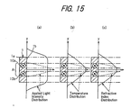
- the applied light intensity distribution in the y-axis direction on these crystal side surfaces 1a and 1b is uniform all over the side surface as indicated by a solid line in FIG. 15(a).
- the applied light intensity tends to be low at the upper and lower ends of the crystal side surfaces 1a and 1b.
- the temperature distribution in the y-axis direction within the crystal is a distribution having a maximum value at the crystal center portion as indicated by a solid line in FIG. 15(b), because of heat conduction in the diametrical direction (y-axis direction) of a cross section of the laser light path.
- the refractive index distribution in the y-axis direction within the crystal is also a nonuniform distribution, as shown in FIG. 15(c), in accordance with this temperature distribution.
- YAG laser light 10 is condensed or contorted in the YAG laser light paths 10a, 10b within the crystal, resulting in a deterioration of light quality. Condensation of the YAG laser light 10 within the crystal may make the diameter of the YAG laser light 10 smaller than a predetermined diameter. The decrease in the diameter of the YAG laser light 10 may lower the oscillation efficiency, or may further burn out the crystal 1.
- a portion contributing to optical excitation of the laser medium doped into the crystal 1 is only a region A of the two YAG laser light paths 10a and 10b, and the other portion is of no use.
- the applied light density in the laser light path region A is low.
- the utilization efficiency of the semiconductor laser light 9 is poor, and the semiconductor laser output is great relative to the necessary YAG laser output.
- the portion other than the laser light path region A in the crystal 1 is a portion necessary as a mechanism for cooling and maintaining the crystal 1, and necessary for the optical axis adjustment of the YAG laser light 10.
- the present invention has been accomplished in light of the foregoing problems, and is aimed at providing a solid state laser apparatus having a high utilization efficiency of semiconductor laser light, and being capable of uniformizing the refractive index distribution in the width direction of side surfaces of a slab-shaped crystal in the laser light path region of the slab-shaped crystal.
- Document JP 5-21869 discloses a solid-state laser apparatus having the features of the preamble part of claim 1. Further, document JP 5-90670 discloses a solid state laser having a semiconductor array as exciting light source on either side of the solid-state laser crystal creating a light intensity distribution in the solid-state laser crystal which is single peaked and concentrated in the laser light path region of the solid-state laser crystal. Document JP 11-214776 discloses a solid-state laser excited by a laser diode wherein a cylindrical lens on either side of the solid-state laser crystal focuses the excitation light into the laser light path region of the solid-state laser crystal.
- the solid state laser apparatus of the present invention which attains the above object, is characterized by the following features:
- semiconductor laser light is concentrated and applied onto the laser light path region and its neighborhood.
- the utilization efficiency of the semiconductor laser light is increased, and when the same solid state laser output as before is to be obtained, the semiconductor laser output (input to the crystal) can be made smaller than before. In other words, when the same semiconductor laser output as before is given, a greater solid state laser output than before can be obtained.
- the concentrated applied light intensity distribution in the side surface width direction perpendicular to the plane of the zigzag path of the solid state laser light within the crystal is formed as a double-peak distribution having the maximum values at the opposite sides, with respect to the axis of the laser resonator, of the laser light path region of the crystal, or in their neighborhoods.
- the temperature distribution in the side surface width direction perpendicular to the plane of the zigzag path of the solid state laser light within the crystal is a uniform distribution in the laser light path region.
- the refractive index distribution in the side surface width direction perpendicular to the plane of the zigzag path of the solid state laser light within the crystal is also a uniform distribution in the laser light path region. Consequently, the solid state laser light is prevented from being condensed or contorted in the solid state laser light paths within the crystal owing to the thermal lens effect, so that the quality of the solid state laser light is improved.
- FIG. 1 is a perspective view showing the configuration of a YAG laser apparatus according to a first embodiment of the present invention.
- FIG. 2 is a cross sectional view of the above YAG laser apparatus.
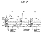
- FIGS. 3(a) to 3(c) are explanation drawings showing the concentrated applied light intensity distribution, temperature distribution, and refractive index distribution in the side surface width direction of the slab-shaped YAG crystal of the above YAG laser apparatus.
- a YAG laser apparatus 20 a solid state laser apparatus, has a pair of LD apparatuses 22 as an exciting light source, and these LD apparatuses 22 are disposed so as to be opposed to both side surfaces 21a and 21b of a slab-shaped YAG crystal (hereinafter referred to simply as a crystal) 21.
- An output mirror 23 and a total reflection mirror 24 are provided parallel on one side in the longitudinal direction (x-axis direction) of the crystal 21, while a turnback total reflection mirror 25 and a turnback total reflection mirror 26 are provided parallel on the other side in the longitudinal direction of the crystal 21.
- These mirrors 23, 24, 25 and 26 constitute a resonator.
- the illustrated example shows a YAG laser light path in the crystal as two axes, a YAG laser light path 30a and a YAG laser light path 30b (laser light axes 30a-1 and 30b-1).
- the LD apparatus 22 comprises many cooling blocks 28 stacked in the x-axis direction, each of the cooling blocks 28 having an LD device 27 fixed to the side surface thereof.
- a water channel (not shown) for flowing cooling water, which cools the LD device 27, is formed in the cooling block 28.
- the LD device 27 used here comprises several tens of active media arranged one-dimensionally (i.e., a one-dimensional LD array device), each of the active media having a cross sectional area of several micrometers x several hundred micrometers.
- the LD devices 27 are stacked, together with the cooling blocks 28, to constitute a two-dimensional LD array device.
- semiconductor laser light 29 is emitted from the respective LD devices 27, and this laser light 29 is directed, as exciting light, at the opposite side surfaces 21a and 21b of the crystal 21.
- the laser medium doped into the crystal is excited, whereby YAG laser light 30 is issued from the output mirror 23 of the resonator.
- the YAG laser light paths 30a, 30b in the crystal are zigzag optical paths, in which laser light advances in the x-axis direction while being reflected by the opposite side surfaces 21a and 21b in the thickness direction (z-axis direction) of the crystal 21, because the entrance and exit of the crystal 21 (the opposite end surfaces in the x-axis direction) have Brewster's angle.
- the entrance and exit of the crystal 21 have Brewster's angle.
- An concave lens 31 and a pair of reflecting mirrors, 32 and 33, are interposed between the LD apparatus 22 and the crystal 21.
- the concave lens 31 is disposed ahead of the LD apparatus 22, and diffuses semiconductor laser light 29, emitted from the LD apparatus 22, in the side surface width direction (y-axis direction) of the crystal 21.
- the pair of reflecting mirrors 32 and 33 are interposed between the concave lens 31 and the crystal 21, and have reflecting surfaces 32a and 33a opposed to each other in the y-axis direction.
- the spacing between these reflecting surfaces 32a and 33a in the y-axis direction gradually narrows from base end portions of the reflecting mirrors facing the concave lens toward front end portions of the reflecting mirrors facing the crystal and, at the front ends of the reflecting mirrors, becomes a spacing corresponding to a laser light path region A of the crystal 21 and its neighborhood.
- the concentrated applied light intensity distribution in the y-axis direction on the side surfaces 21a, 21b of the crystal 21 is a double-peak distribution having maximum values P 1 and P 2 at opposite end portions A 1 and A 2 of the laser light path region A of the crystal, or in their neighborhoods.
- FIG. 3(a) shows the presence of the maximum values P 1 and P 2 at the opposite end portions A 1 and A 2 of the laser light path region A.
- the maximum values P 1 and P 2 are present in the neighborhoods of the opposite end portions A 1 and A 2 , and the optimum positions may be suitably set based on analysis or experiments.
- the concentrated applied light intensity distribution in the y-axis direction on the side surfaces 21a, 21b of the crystal 21 is neither a double-peak distribution having the maximum values P 1 and P 2 at the centers of the cross sections of the YAG laser light paths 30a and 30b (i.e., the laser light axes 30a-1 and 30b-1), nor a single-peak distribution having a maximum value midway between the laser light path 30a and the laser light path 30b, but is a double-peak distribution having the maximum values P 1 and P 2 at the opposite end portions A 1 and A 2 of the laser light path region A, or in their neighborhoods.
- the temperature distribution in the y-axis direction within the crystal is a uniform distribution in the laser light path region A.
- the refractive index distribution in the y-axis direction within the crystal is also a uniform distribution in the laser light path region A, as shown in FIG. 3(c).
- the semiconductor laser light 29 is concentrated and applied onto the laser light path region A and its neighborhood.
- the utilization efficiency of the semiconductor laser light 29 is increased, and when the same YAG laser output as before is to be obtained, the semiconductor laser output (input to the crystal) can be made smaller than before. In other words, when the same semiconductor laser output as before is given, a greater YAG laser output than before can be obtained.
- the concentrated applied light intensity distribution in the y-axis direction of the crystal 21 is a double-peak distribution having the maximum values P 1 and P 2 at the opposite end portions A 1 and A 2 of the laser light path region A of the crystal 21, or in their neighborhoods.
- the temperature distribution in the y-axis direction within the crystal is a uniform distribution in the laser light path region A.
- the refractive index distribution in the y-axis direction within the crystal is also a uniform distribution in the laser light path region A. Consequently, the YAG laser light 30 is prevented from being condensed or contorted in the YAG laser light paths 30a, 30b within the crystal owing to the thermal lens effect, so that the quality of the YAG laser light 30 is improved.
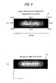
- FIGS. 4(a) and 4(b) show an example of analysis made when laser light is concentrated and applied such that the concentrated applied light intensity distribution is a double-peak distribution (i.e., laser light is applied onto a 16 mm width relative to the crystal width of 20 mm).
- the differences in color density represent differences in temperature
- the numerical values in the drawings represent temperatures (°C).
- the temperature distribution in the y-axis direction within the crystal is a uniform distribution in the laser light path region.
- the refractive index distribution in the y-axis direction within the crystal is also a uniform distribution in the laser light path region, as shown in FIG. 4(b).
- the above descriptions show the laser light path within the crystal as two axes, but needless to say, this is not restrictive.
- the invention according to the present embodiment 1 can be applied to the laser light path of a single axis or three or more axes.
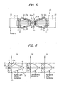
- FIG. 5 shows a one-axis laser light path.
- the concentrated applied light intensity distribution in the y-axis direction on the side surfaces 21a, 21b of the crystal 21 is a double-peak distribution having the maximum values P 1 and P 2 at the opposite end portions A 1 and A 2 of the laser light path region A of the crystal 21, or in their neighborhoods.
- the temperature distribution in the y-axis direction within the crystal is a uniform distribution in the laser light path region A.
- the refractive index distribution in the y-axis direction within the crystal is also a uniform distribution in the laser light path region A, as shown in FIG. 6(c).
- laser light is concentrated by suitable light concentrating/applying means to achieve a concentrated applied light intensity distribution having a maximum value at the center in the y-axis direction in the laser light path region A, as indicated by dashed lines in FIG. 15 (a).
- the temperature distribution is also a distribution having a maximum value at the center in the y-axis direction in the laser light path region A, as indicated by dashed lines in FIG. 15(b).
- the refractive index distribution is also a distribution having a maximum value at the center in the y-axis direction in the laser light path region A, as indicated by dashed lines in FIG. 15(c).
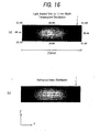
- FIGS. 16(a) and 16(b) show an example of analysis made when semiconductor laser light is concentrated and applied only to an 11 mm width.
- the temperature distribution is a distribution having a maximum value at the center in the y-axis direction in the laser light path region, as shown in FIG. 16(a).
- the refractive index distribution is also a distribution having a maximum value at the center in the y-axis direction in the laser light path region, as shown in FIG. 16(b).
- the concave lens 31 is used to diffuse the semiconductor laser light 29 once.
- the concave lens need not be used, and the use of the reflecting mirrors alone suffices.
- the apparatus is upsized, and the semiconductor laser light attenuates greatly by the time it arrives at the crystal.
- these problems are solved by using the concave lens 31.
- the acquisition of an LD apparatus which can emit laser light with a sufficiently large spread angle, would be able to bring the LD apparatus and the crystal close to each other, even with the use of the reflecting mirrors alone without the use of the concave lens.
- upsizing of the apparatus would not be induced.
- FIG. 7 is a perspective view showing the configuration of a YAG laser apparatus according to a second embodiment of the present invention.
- FIG. 8 is a cross sectional view of the above YAG laser apparatus.
- a YAG laser apparatus 40 As shown in FIGS. 7 and 8, a YAG laser apparatus 40 according to the present embodiment has a duct lens 41 interposed, as light concentrating/applying means, between an LD apparatus 22 and a slab-shaped YAG crystal 21.
- the duct lens 41 is a quartz lens whose base end surface 41a facing the LD apparatus is a concave surface, and whose surfaces 41b and 41c opposed to each other in the y-axis direction are reflecting surfaces each provided with a reflective coating such as gold coating.
- the spacing between these reflecting surfaces 41b and 41c in the y-axis direction gradually narrows from a base end portion of the duct lens facing the LD apparatus toward a front end portion of the duct lens facing the crystal and, at the front end surface 41d of the duct lens, becomes a width corresponding to a laser light path region A of the crystal 21 and its neighborhood.
- laser light 29 emitted from the LD apparatus 22 is concentrated and applied by the duct lens 41 to the laser light path region A of the crystal 21 and its neighborhood.
- the concentrated applied light intensity distribution in the y-axis direction on the side surfaces 21a, 21b of the crystal 21 is a double-peak distribution having maximum values at opposite end portions of the laser light path region A of the crystal 21, or in their neighborhoods (see FIGS. 3(a) to 3(c)).
- the same actions and effects as in the first embodiment are obtained. That is, the laser light 29 is applied onto the laser light path region A and its neighborhood. Thus, the utilization efficiency of the semiconductor laser light 29 is increased, and when the same YAG laser output as before is to be obtained, the semiconductor laser output (input to the crystal) can be made smaller than before. In other words, when the same semiconductor laser output as before is given, a greater YAG laser output than before can be obtained.
- the concentrated applied light intensity distribution in the y-axis direction of the crystal 21 is a double-peak distribution having the maximum values at the opposite end portions of the laser light path region A of the crystal 21, or in their neighborhoods.
- the temperature distribution in the y-axis direction within the crystal is a uniform distribution in the laser light path region A.
- the refractive index distribution in the y-axis direction within the crystal is also a uniform distribution in the laser light path region A. Consequently, YAG laser light 30 is prevented from being condensed or contorted in YAG laser light paths 30a, 30b within the crystal owing to the thermal lens effect, so that the quality of the YAG laser light 30 is improved.
- the invention according to the present second embodiment is not restricted to the two-axis laser light path, but can also be applied to the laser light path of a single axis or three or more axes, although this is not illustrated.
- FIG. 9 is a perspective view showing the configuration of a YAG laser apparatus according to a third embodiment of the present invention.
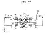
- FIG. 10 is a cross sectional view of the above YAG laser apparatus.
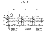
- FIGS. 11(a) to 11(c) are explanation drawings showing the concentrated applied light intensity distribution, temperature distribution, and refractive index distribution in the side surface width direction of a slab-shaped YAG crystal of the above-described YAG laser apparatus.
- a YAG laser apparatus 50 in a YAG laser apparatus 50 according to the present third embodiment, as shown in FIGS. 9 and 10, two cylindrical lenses 51 and 52 are interposed, as light concentrating/applying means, between an LD apparatus 22 and a slab-shaped YAG crystal 21.
- the cylindrical lenses 51, 52 are in a semicylindrical form.
- the cylindrical lenses 51, 52 are arranged parallel such that their longitudinal direction (y-axis direction) is along the longitudinal direction (y-axis direction) of the crystal 21.
- Laser light 29 emitted from the LD apparatus 22 is concentrated and applied by these cylindrical lenses 51 and 52 onto a laser light path region A of the crystal 21 and its neighborhood.
- the concentrated applied light intensity distribution in the y-axis direction on the side surfaces 21a, 21b of the crystal 21 is a double-peak distribution having maximum values P 1 and P 2 at opposite end portions A 1 and A 2 of the laser light path region A of the crystal 21, or in their neighborhoods.
- the cylindrical lenses are not limited in number to two, but their combination or focal lengths may be selected suitably, whereby the above-mentioned double-peak concentrated applied light intensity distribution can be obtained.
- Forming the concentrated applied light intensity distribution as a double-peak distribution can compensate for decreases in the light intensities at the opposite end portions A 1 and A 2 of the laser light path region A, compared with the light intensity at the center of the laser light path region A, due to heat conduction.
- the temperature distribution in the y-axis direction within the crystal is a uniform distribution in the laser light path region A.
- the refractive index distribution in the y-axis direction within the crystal is also a uniform distribution in the laser light path region A, as shown in FIG. 11(c).
- laser light 29 is applied onto the laser light path region A and its neighborhood.
- the utilization efficiency of the semiconductor laser light 29 is increased, and when the same YAG laser output as before is to be obtained, the semiconductor laser output (input to the crystal) can be made smaller than before. In other words, when the same semiconductor laser output as before is given, a greater YAG laser output than before can be obtained.
- the concentrated applied light intensity distribution in the y-axis direction of the crystal 21 is a double-peak distribution having the maximum values P 1 and P 2 at the opposite end portions A 1 and A 2 of the laser light path region A of the crystal 21, or in their neighborhoods.
- the temperature distribution in the y-axis direction within the crystal is a uniform distribution in the laser light path region A.
- the refractive index distribution in the y-axis direction within the crystal is also a uniform distribution in the laser light path region A. Consequently, the YAG laser light 30 is prevented from being condensed or contorted in the YAG laser light paths 30a, 30b within the crystal owing to the thermal lens effect, so that the quality of the YAG laser light 30 is improved.
- the above descriptions show the laser light path within the crystal as two axes, but needless to say, this is not restrictive.
- the invention according to the present embodiment can also be applied to the laser light path of a single axis or three or more axes.
- FIG. 12 shows a one-axis laser light path.
- the concentrated applied light intensity distribution in the y-axis direction on the side surfaces 21a, 21b of the crystal 21 is a double-peak distribution having the maximum values P 1 and P 2 at the opposite end portions A 1 and A 2 of the laser light path region A of the crystal 21, or in their neighborhoods.
- the temperature distribution in the y-axis direction within the crystal is a uniform distribution in the laser light path region A.
- the refractive index distribution in the y-axis direction within the crystal is also a uniform distribution in the laser light path region A, as shown in FIG. 12(c).
- the present embodiment A comparison will be made between the present embodiment and the aforementioned first embodiment.
- laser light is concentrated and applied by the cylindrical lenses 51, 52 onto the laser light path region A and its neighborhood. Thus, light tends to leak to the outside of this range.
- laser light is concentrated and applied by the reflecting mirrors 32, 33 onto the laser light path region A and its neighborhood. Thus, light minimally leaks to the outside of this range.
- the first embodiment has an advantage over the present embodiment.
- the concentrated applied light intensity distribution in the y-axis direction of the crystal 21 is formed by optical means as a double-peak distribution having the maximum values at the opposite end portions of the laser light path region A of the crystal 21, or in their neighborhoods.
- semiconductor laser light may be electrically controlled to obtain such a double-peak concentrated applied light intensity distribution.
- the solid state laser apparatus of the present invention has a high utilization efficiency of semiconductor laser light, uniformizes the refractive index distribution in the side surface width direction of a slab-shaped crystal in the laser light path region of the slab-shaped crystal, and is useful for use in material processing, such as drilling, cutting or welding, and surface treatment, such as surface modification or marking.
Landscapes
- Physics & Mathematics (AREA)
- Electromagnetism (AREA)
- Engineering & Computer Science (AREA)
- Plasma & Fusion (AREA)
- Optics & Photonics (AREA)
- Lasers (AREA)
Claims (4)
- Feststofflaservorrichtung (20), die eine Laserdiodenvorrichtung (22) als anregende Lichtquelle aufweist und geeignet ist, von der Laserdiodenvorrichtung (22) emittiertes Laserlicht als anregendes Licht auf Seitenflächen (21a, 21b) eines plattenförmigen Kristalls (21) zu lenken, um Feststofflaserlicht (30) zu emittieren, wobei das Feststofflaserlicht im Kristall (21) zick-zackreflektiert wird, wobei die Seitenflächen senkrecht zur Ebene des Zick-Zack-Wegs liegen, und
wobei die Feststofflaservorrichtung (20) eine Lichtkonzentrations-/Anwendungsvorrichtung (31, 32, 33; 41; 51, 52) aufweist, um das aus der Laserdiodenvorrichtung (22) emittierte anregende Laserlicht (29) auf einen Feststofflaserlichtwegbereich (A) des plattenförmigen Kristalls (21) und seine Umgebung zu konzentrieren und anzuwenden,
dadurch gekennzeichnet, dass:die Lichtkonzentrations-/Anwendungsvorrichtung (31, 32, 33; 41; 51, 52) eine Vorrichtung zum Konzentrieren und Anwenden des aus der Laserdiodenvorrichtung (22) emittierten anregenden Laserlichts (29) auf einen Laserlichtwegbereich (A) des plattenförmigen Kristalls (21) und dessen Umgebung und zum Ausbilden einer konzentrierten anregenden Lichtintensitätsverteilung in Breitenrichtung der Seitenfläche (21a, 21b) senkrecht zur Ebene des Zick-Zack-Wegs des Feststofflaserlichts im Kristall als Verteilung mit doppelter Spitze ist, die Maximalwerte (P1, P2) auf in Bezug zur Achse des Laserresonators gegenüberliegenden Seiten (A1, A2) des Feststofflaserlichtwegbereichs (A) des plattenförmigen Kristalls (21) oder in dessen Umgebungen aufweist, so dass eine Temperaturverteilung in der Breitenrichtung der Seitenflächen senkrecht zur Ebene des Zick-Zack-Wegs des Feststofflaserlichts im plattenförmigen Kristall im Feststofflaserlichtwegbereich gleichförmig ist. - Feststofflaservorrichtung (20) nach Anspruch 1, miteiner konkaven Linse (31) zum Diffundieren des aus der Laserdiodenvorrichtung (22) emittierten anregenden Laserlichts (29) in einer Breitenrichtung der Seitenfläche (21a, 21b) senkrecht zur Ebene des Zick-Zack-Wegs des Feststofflaserlichts im Kristall; undeinem Paar von reflektierenden Spiegeln (32, 33), die so angeordnet sind, dass deren reflektierenden Oberflächen (32a, 33a) in einer Breitenrichtung der Seitenfläche (21a, 21b) senkrecht zur Ebene des Zick-Zack-Wegs des Feststofflaserlichts im Kristall einander gegenüberliegen und dass der Abstand zwischen den reflektierenden Oberflächen (32a, 33a) sich allmählich von Basisendabschnitten der reflektierenden Spiegel (32, 33), die der konkaven Linse (31) zugewandt sind, zu den Vorderendabschnitten der reflektierenden Spiegel (32, 33), die dem plattenförmigen Kristall (21) zugewandt sind, verengt und an den Vorderendabschnitten der reflektierenden Spiegel (32, 33) zu einem Abstand wird, der einem Feststofflaserlichtwegbereich (A) des plattenförmigen Kristalls (21) und dessen Umgebung entspricht, und dadurch gekennzeichnet, dassdas aus der Laserdiodenvorrichtung (22) emittierte anregende Laserlicht (29) von der konkaven Linse (31) diffundiert wird, dann von den reflektierenden Spiegeln (32, 33) reflektiert wird und auf den Feststofflaserlichtwegbereich (A) des plattenförmigen Kristalls (21) und dessen Umgebung konzentriert und angewendet wird, wobei eine konzentrierte anregende Lichtintensitätsverteilung in der Breitenrichtung der Seitenfläche (21a, 21b) senkrecht zur Ebene des Zick-Zack-Wegs des Feststofflaserlichts im Kristall als Verteilung mit doppelter Spitze ausgebildet wird, die Maximalwerte (P1, P2) auf in Bezug zur Achse des Laserresonators gegenüberliegenden Seiten (A1, A2) des Feststofflaserlichtwegbereichs (A) des plattenförmigen Kristalls (21) oder in dessen Umgebung aufweist, so dass eine Temperaturverteilung in der Breitenrichtung der Seitenfläche senkrecht zur Ebene des Zick-Zack-Wegs des Feststofflaserlichts im plattenförmigen Kristall im Feststofflaserlichtwegbereich gleichförmig ist.
- Feststofflaservorrichtung (40) nach Anspruch 1, miteiner Führungslinse (41), die so ausgebildet ist, dass eine Basisendfläche der Führungslinse (41), die der Laserdiodenvorrichtung (22) zugewandt ist, eine konkave Oberfläche (41a) ist, die Oberflächen der Führungslinse (41), die einander in einer Breitenrichtung der Seitenfläche (21a, 21b) senkrecht zur Ebene des Zick-Zack-Wegs des Feststofflaserlichts im Kristall gegenüberliegen, reflektierende Oberflächen (41b, 41c) sind und der Abstand zwischen den reflektierenden Oberflächen (41b, 41c) sich allmählich von einem Basisendabschnitt der Führungslinse (41), welcher der Laserdiodenvorrichtung (22) zugewandt ist, zu einem Vorderendabschnitt der Führungslinse (41), welcher dem plattenförmigen Kristall (21) zugewandt ist, verengt und an einer Vorderendfläche der Führungslinse (41) zu einer Breite wird, die einem Feststofflaserlichtwegbereich (A) des plattenförmigen Kristalls (21) und dessen Umgebung entspricht, und dadurch gekennzeichnet, dassdas aus der Laserdiodenvorrichtung (22) emittierte anregende Laserlicht (29) von der Führungslinse (41) auf den Feststofflaserlichtwegbereich (A) des plattenförmigen Kristalls (21) und dessen Umgebung konzentriert und angewendet wird, wodurch eine konzentrierte anregende Lichtintensitätsverteilung in der Breitenrichtung der Seitenfläche (21a, 21b) senkrecht zur Achsenebene des Zick-Zack-Wegs des Feststofflaserlichts im Kristall als Verteilung mit zwei Spitzen ausgebildet wird, die Maximalwerte (P1, P2) auf in Bezug zur Achse des Laserresonators gegenüberliegenden Seiten (A1, A2) des Feststofflaserlichtwegbereichs (A) des plattenförmigen Kristalls (21) oder in dessen Umgebungen aufweist, so dass eine Temperaturverteilung in der Breitenrichtung der Seitenfläche senkrecht zur Ebene des Zick-Zack-Wegs des Feststofflaserlichts im plattenförmigen Kristall in dem Feststofflaserlichtwegbereich gleichförmig ist.
- Feststofflaservorrichtung (50) nach Anspruch 1, dadurch gekennzeichnet, dass:eine Vielzahl von zylindrischen Linsen (51, 52) parallel angeordnet sind, so dass deren Längsrichtung entlang einer Längsrichtung des plattenförmigen Kristalls (21) liegt; unddas aus der Laserdiodenvorrichtung (22) emittierte anregende Laserlicht (29) von den zylindrischen Linsen (51, 52) auf einen Feststofflaserlichtwegbereich (A) des plattenförmigen Kristalls (21) und dessen Umgebung konzentriert und angewendet wird, wodurch eine konzentrierte anregende Lichtintensitätsverteilung in einer Breitenrichtung der Seitenfläche (21a, 21b) senkrecht zur Ebene des Zick-Zack-Wegs des Feststofflaserlichts im Kristall als Verteilung mit doppelter Spitze ausgebildet wird, die Maximalwerte (P1, P2) auf in Bezug zur Achse des Laserresonators gegenüberliegenden Seiten (A1, A2) des Feststofflaserlichtwegbereichs (A) des plattenförmigen Kristalls (21) oder in dessen Umgebungen aufweist, so dass eine Temperaturverteilung in der Breitenrichtung der Seitenfläche senkrecht zur Ebene des Zick-Zack-Wegs des Feststofflaserlichts im plattenförmigen Kristall im Feststofflaserlichtwegbereich gleichförmig ist.
Applications Claiming Priority (3)
| Application Number | Priority Date | Filing Date | Title |
|---|---|---|---|
| JP2000116335 | 2000-04-18 | ||
| JP2000116335A JP2001298231A (ja) | 2000-04-18 | 2000-04-18 | 固体レーザ装置 |
| PCT/JP2001/003218 WO2001080382A1 (en) | 2000-04-18 | 2001-04-16 | Solid laser apparatus |
Publications (3)
| Publication Number | Publication Date |
|---|---|
| EP1198039A1 EP1198039A1 (de) | 2002-04-17 |
| EP1198039A4 EP1198039A4 (de) | 2004-07-07 |
| EP1198039B1 true EP1198039B1 (de) | 2007-09-12 |
Family
ID=18627808
Family Applications (1)
| Application Number | Title | Priority Date | Filing Date |
|---|---|---|---|
| EP01921844A Expired - Lifetime EP1198039B1 (de) | 2000-04-18 | 2001-04-16 | Festkörperlaser |
Country Status (5)
| Country | Link |
|---|---|
| US (1) | US6721347B2 (de) |
| EP (1) | EP1198039B1 (de) |
| JP (1) | JP2001298231A (de) |
| DE (1) | DE60130423T2 (de) |
| WO (1) | WO2001080382A1 (de) |
Families Citing this family (3)
| Publication number | Priority date | Publication date | Assignee | Title |
|---|---|---|---|---|
| JP2006516810A (ja) * | 2003-01-24 | 2006-07-06 | トルンプフ インコーポレイテッド | サイドポンプファイバレーザ |
| FR2885743B1 (fr) * | 2005-05-10 | 2009-07-10 | Commissariat Energie Atomique | Dispositif de pompage optique |
| EP2184818A1 (de) * | 2008-11-10 | 2010-05-12 | High Q Technologies GmbH | Laserpumpanordnung und Laserpumpverfahren mit Strahlhomogenisierung |
Family Cites Families (13)
| Publication number | Priority date | Publication date | Assignee | Title |
|---|---|---|---|---|
| JPH0521869A (ja) * | 1991-07-12 | 1993-01-29 | Nec Corp | 固体レーザ発振装置 |
| JPH0590670A (ja) * | 1991-09-30 | 1993-04-09 | Hoya Corp | 半導体レーザ側面励起固体レーザ装置 |
| JP2872855B2 (ja) * | 1992-02-19 | 1999-03-24 | ファナック株式会社 | レーザ発振器 |
| US5307430A (en) * | 1992-11-30 | 1994-04-26 | The United States Of America As Represented By The United States Department Of Energy | Lensing duct |
| JPH06310782A (ja) * | 1993-04-27 | 1994-11-04 | Hitachi Ltd | スラブ形固体レーザ装置 |
| US5515394A (en) * | 1993-05-28 | 1996-05-07 | Zhang; Tong | One dimensional beam expanding cavity for diode-pumped solid-state lasers |
| US5555254A (en) * | 1993-11-05 | 1996-09-10 | Trw Inc. | High brightness solid-state laser with zig-zag amplifier |
| JPH1117252A (ja) * | 1997-06-26 | 1999-01-22 | Mitsubishi Electric Corp | 半導体励起固体レーザ装置 |
| JPH1187816A (ja) | 1997-09-12 | 1999-03-30 | Fanuc Ltd | Ld励起固体レーザ発振装置 |
| US5974061A (en) * | 1997-12-19 | 1999-10-26 | Raytheon Company | Laser pump cavity apparatus with improved thermal lensing control, cooling, and fracture strength and method |
| JPH11214776A (ja) * | 1998-01-23 | 1999-08-06 | Mitsubishi Heavy Ind Ltd | Ld励起固体レーザ |
| US6560397B1 (en) * | 2000-10-30 | 2003-05-06 | Fraunhofer, Usa | Optical system for varying the beam width using non-imaging optics |
| US6625193B2 (en) * | 2001-01-22 | 2003-09-23 | The Boeing Company | Side-pumped active mirror solid-state laser for high-average power |
-
2000
- 2000-04-18 JP JP2000116335A patent/JP2001298231A/ja not_active Withdrawn
-
2001
- 2001-04-16 DE DE60130423T patent/DE60130423T2/de not_active Expired - Fee Related
- 2001-04-16 US US09/926,776 patent/US6721347B2/en not_active Expired - Fee Related
- 2001-04-16 WO PCT/JP2001/003218 patent/WO2001080382A1/ja not_active Ceased
- 2001-04-16 EP EP01921844A patent/EP1198039B1/de not_active Expired - Lifetime
Also Published As
| Publication number | Publication date |
|---|---|
| US20020136257A1 (en) | 2002-09-26 |
| EP1198039A1 (de) | 2002-04-17 |
| EP1198039A4 (de) | 2004-07-07 |
| WO2001080382A1 (en) | 2001-10-25 |
| DE60130423D1 (de) | 2007-10-25 |
| DE60130423T2 (de) | 2008-06-12 |
| US6721347B2 (en) | 2004-04-13 |
| JP2001298231A (ja) | 2001-10-26 |
Similar Documents
| Publication | Publication Date | Title |
|---|---|---|
| JP3589299B2 (ja) | ビーム整形装置 | |
| EP1160940B1 (de) | Optischer Verstärker mit stabförmigen, von der Endseite gepumpten Verstärkungsmedium | |
| US5661738A (en) | Solid-state laser amplifying apparatus and solid-state laser apparatus capable of oscillating high-power laser beam under stable condition | |
| US6873633B2 (en) | Solid-state laser | |
| KR101857751B1 (ko) | 슬랩 고체 레이저 증폭장치 | |
| US6118804A (en) | Laser amplification system | |
| US6351477B1 (en) | Optically pumped intensifying agent, in particular a solid intensifying agent | |
| EP1198039B1 (de) | Festkörperlaser | |
| JP2000082860A (ja) | 固体レーザ装置 | |
| JP2000077750A (ja) | 固体レーザ装置 | |
| JPH1168197A (ja) | 半導体レーザ励起固体レーザ装置 | |
| JP3391235B2 (ja) | 半導体レーザ励起固体レーザ増幅装置 | |
| EP1039594A1 (de) | Lichtverstärker, gerät und verfahren zür lichtverstärkung | |
| JP2000277837A (ja) | 固体レーザ装置 | |
| JP2009194176A (ja) | 固体レーザ装置及びレーザ加工方法 | |
| JP2004179412A (ja) | 半導体レーザ励起固体レーザ装置並びにその製造方法 | |
| KR100257401B1 (ko) | 출력조절식 레이저 광 발생장치 | |
| JP7763656B2 (ja) | レーザ媒質ユニット、レーザ増幅装置及びレーザ発振装置 | |
| JPH10261825A (ja) | 半導体レーザ光整形光学系及び半導体レーザ励起固体レーザ装置 | |
| US20020051480A1 (en) | Laser diode excitation slab type solid-state laser | |
| JP4001077B2 (ja) | 固体レーザ増幅装置及び固体レーザ装置 | |
| JPS61212078A (ja) | スラブ形レ−ザ装置 | |
| JPH08274393A (ja) | スラブレーザおよびレーザ加工機 | |
| JPH07307507A (ja) | 固体レーザ | |
| JPH10135539A (ja) | レーザ装置 |
Legal Events
| Date | Code | Title | Description |
|---|---|---|---|
| PUAI | Public reference made under article 153(3) epc to a published international application that has entered the european phase |
Free format text: ORIGINAL CODE: 0009012 |
|
| 17P | Request for examination filed |
Effective date: 20011218 |
|
| AK | Designated contracting states |
Kind code of ref document: A1 Designated state(s): AT BE CH CY DE DK ES FI FR GB GR IE IT LI LU MC NL PT SE TR |
|
| RBV | Designated contracting states (corrected) |
Designated state(s): DE FR GB |
|
| A4 | Supplementary search report drawn up and despatched |
Effective date: 20040526 |
|
| 17Q | First examination report despatched |
Effective date: 20040604 |
|
| 17Q | First examination report despatched |
Effective date: 20040604 |
|
| GRAP | Despatch of communication of intention to grant a patent |
Free format text: ORIGINAL CODE: EPIDOSNIGR1 |
|
| RTI1 | Title (correction) |
Free format text: SOLID STATE LASER APPARATUS |
|
| RIN1 | Information on inventor provided before grant (corrected) |
Inventor name: KATO, MASAHIRO,MITSUBISHI HEAVY INDUSTRIES, LTD. Inventor name: MIKI, SUSUMU,MITSUBISHI HEAVY INDUSTRIES, LTD. Inventor name: MIZUI, JYUNICHI,MITSUBISHI HEAVY INDUSTRIES, LTD. Inventor name: AKABA, TAKASHI,MITSUBISHI HEAVY INDUSTRIES, LTD. |
|
| GRAS | Grant fee paid |
Free format text: ORIGINAL CODE: EPIDOSNIGR3 |
|
| GRAA | (expected) grant |
Free format text: ORIGINAL CODE: 0009210 |
|
| AK | Designated contracting states |
Kind code of ref document: B1 Designated state(s): DE FR GB |
|
| REG | Reference to a national code |
Ref country code: GB Ref legal event code: FG4D |
|
| REF | Corresponds to: |
Ref document number: 60130423 Country of ref document: DE Date of ref document: 20071025 Kind code of ref document: P |
|
| ET | Fr: translation filed | ||
| PLBE | No opposition filed within time limit |
Free format text: ORIGINAL CODE: 0009261 |
|
| STAA | Information on the status of an ep patent application or granted ep patent |
Free format text: STATUS: NO OPPOSITION FILED WITHIN TIME LIMIT |
|
| 26N | No opposition filed |
Effective date: 20080613 |
|
| PGFP | Annual fee paid to national office [announced via postgrant information from national office to epo] |
Ref country code: DE Payment date: 20090409 Year of fee payment: 9 Ref country code: FR Payment date: 20090417 Year of fee payment: 9 |
|
| PGFP | Annual fee paid to national office [announced via postgrant information from national office to epo] |
Ref country code: GB Payment date: 20090415 Year of fee payment: 9 |
|
| GBPC | Gb: european patent ceased through non-payment of renewal fee |
Effective date: 20100416 |
|
| REG | Reference to a national code |
Ref country code: FR Ref legal event code: ST Effective date: 20101230 |
|
| PG25 | Lapsed in a contracting state [announced via postgrant information from national office to epo] |
Ref country code: DE Free format text: LAPSE BECAUSE OF NON-PAYMENT OF DUE FEES Effective date: 20101103 |
|
| PG25 | Lapsed in a contracting state [announced via postgrant information from national office to epo] |
Ref country code: GB Free format text: LAPSE BECAUSE OF NON-PAYMENT OF DUE FEES Effective date: 20100416 |
|
| PG25 | Lapsed in a contracting state [announced via postgrant information from national office to epo] |
Ref country code: FR Free format text: LAPSE BECAUSE OF NON-PAYMENT OF DUE FEES Effective date: 20100430 |