EP1198003A1 - Semiconductor device, method of manufacture thereof, circuit board, and electronic device - Google Patents
Semiconductor device, method of manufacture thereof, circuit board, and electronic device Download PDFInfo
- Publication number
- EP1198003A1 EP1198003A1 EP01915722A EP01915722A EP1198003A1 EP 1198003 A1 EP1198003 A1 EP 1198003A1 EP 01915722 A EP01915722 A EP 01915722A EP 01915722 A EP01915722 A EP 01915722A EP 1198003 A1 EP1198003 A1 EP 1198003A1
- Authority
- EP
- European Patent Office
- Prior art keywords
- resin layer
- semiconductor device
- resin
- interconnect
- aggregate
- Prior art date
- Legal status (The legal status is an assumption and is not a legal conclusion. Google has not performed a legal analysis and makes no representation as to the accuracy of the status listed.)
- Granted
Links
Images







Classifications
-
- H—ELECTRICITY
- H10—SEMICONDUCTOR DEVICES; ELECTRIC SOLID-STATE DEVICES NOT OTHERWISE PROVIDED FOR
- H10W—GENERIC PACKAGES, INTERCONNECTIONS, CONNECTORS OR OTHER CONSTRUCTIONAL DETAILS OF DEVICES COVERED BY CLASS H10
- H10W74/00—Encapsulations, e.g. protective coatings
- H10W74/01—Manufacture or treatment
-
- H—ELECTRICITY
- H10—SEMICONDUCTOR DEVICES; ELECTRIC SOLID-STATE DEVICES NOT OTHERWISE PROVIDED FOR
- H10W—GENERIC PACKAGES, INTERCONNECTIONS, CONNECTORS OR OTHER CONSTRUCTIONAL DETAILS OF DEVICES COVERED BY CLASS H10
- H10W74/00—Encapsulations, e.g. protective coatings
- H10W74/10—Encapsulations, e.g. protective coatings characterised by their shape or disposition
- H10W74/111—Encapsulations, e.g. protective coatings characterised by their shape or disposition the semiconductor body being completely enclosed
- H10W74/129—Encapsulations, e.g. protective coatings characterised by their shape or disposition the semiconductor body being completely enclosed forming a chip-scale package [CSP]
-
- H—ELECTRICITY
- H10—SEMICONDUCTOR DEVICES; ELECTRIC SOLID-STATE DEVICES NOT OTHERWISE PROVIDED FOR
- H10P—GENERIC PROCESSES OR APPARATUS FOR THE MANUFACTURE OR TREATMENT OF DEVICES COVERED BY CLASS H10
- H10P54/00—Cutting or separating of wafers, substrates or parts of devices
-
- H—ELECTRICITY
- H10—SEMICONDUCTOR DEVICES; ELECTRIC SOLID-STATE DEVICES NOT OTHERWISE PROVIDED FOR
- H10W—GENERIC PACKAGES, INTERCONNECTIONS, CONNECTORS OR OTHER CONSTRUCTIONAL DETAILS OF DEVICES COVERED BY CLASS H10
- H10W70/00—Package substrates; Interposers; Redistribution layers [RDL]
- H10W70/01—Manufacture or treatment
- H10W70/05—Manufacture or treatment of insulating or insulated package substrates, or of interposers, or of redistribution layers
-
- H—ELECTRICITY
- H10—SEMICONDUCTOR DEVICES; ELECTRIC SOLID-STATE DEVICES NOT OTHERWISE PROVIDED FOR
- H10W—GENERIC PACKAGES, INTERCONNECTIONS, CONNECTORS OR OTHER CONSTRUCTIONAL DETAILS OF DEVICES COVERED BY CLASS H10
- H10W70/00—Package substrates; Interposers; Redistribution layers [RDL]
- H10W70/60—Insulating or insulated package substrates; Interposers; Redistribution layers
- H10W70/62—Insulating or insulated package substrates; Interposers; Redistribution layers characterised by their interconnections
- H10W70/65—Shapes or dispositions of interconnections
- H10W70/654—Top-view layouts
- H10W70/656—Fan-in layouts
-
- H—ELECTRICITY
- H10—SEMICONDUCTOR DEVICES; ELECTRIC SOLID-STATE DEVICES NOT OTHERWISE PROVIDED FOR
- H10W—GENERIC PACKAGES, INTERCONNECTIONS, CONNECTORS OR OTHER CONSTRUCTIONAL DETAILS OF DEVICES COVERED BY CLASS H10
- H10W70/00—Package substrates; Interposers; Redistribution layers [RDL]
- H10W70/60—Insulating or insulated package substrates; Interposers; Redistribution layers
- H10W70/67—Insulating or insulated package substrates; Interposers; Redistribution layers characterised by their insulating layers or insulating parts
- H10W70/68—Shapes or dispositions thereof
-
- H—ELECTRICITY
- H10—SEMICONDUCTOR DEVICES; ELECTRIC SOLID-STATE DEVICES NOT OTHERWISE PROVIDED FOR
- H10W—GENERIC PACKAGES, INTERCONNECTIONS, CONNECTORS OR OTHER CONSTRUCTIONAL DETAILS OF DEVICES COVERED BY CLASS H10
- H10W70/00—Package substrates; Interposers; Redistribution layers [RDL]
- H10W70/60—Insulating or insulated package substrates; Interposers; Redistribution layers
- H10W70/67—Insulating or insulated package substrates; Interposers; Redistribution layers characterised by their insulating layers or insulating parts
- H10W70/69—Insulating materials thereof
-
- H—ELECTRICITY
- H10—SEMICONDUCTOR DEVICES; ELECTRIC SOLID-STATE DEVICES NOT OTHERWISE PROVIDED FOR
- H10W—GENERIC PACKAGES, INTERCONNECTIONS, CONNECTORS OR OTHER CONSTRUCTIONAL DETAILS OF DEVICES COVERED BY CLASS H10
- H10W72/00—Interconnections or connectors in packages
- H10W72/01—Manufacture or treatment
- H10W72/012—Manufacture or treatment of bump connectors, dummy bumps or thermal bumps
-
- H—ELECTRICITY
- H10—SEMICONDUCTOR DEVICES; ELECTRIC SOLID-STATE DEVICES NOT OTHERWISE PROVIDED FOR
- H10W—GENERIC PACKAGES, INTERCONNECTIONS, CONNECTORS OR OTHER CONSTRUCTIONAL DETAILS OF DEVICES COVERED BY CLASS H10
- H10W72/00—Interconnections or connectors in packages
- H10W72/01—Manufacture or treatment
- H10W72/0198—Manufacture or treatment batch processes
-
- H—ELECTRICITY
- H10—SEMICONDUCTOR DEVICES; ELECTRIC SOLID-STATE DEVICES NOT OTHERWISE PROVIDED FOR
- H10W—GENERIC PACKAGES, INTERCONNECTIONS, CONNECTORS OR OTHER CONSTRUCTIONAL DETAILS OF DEVICES COVERED BY CLASS H10
- H10W72/00—Interconnections or connectors in packages
- H10W72/20—Bump connectors, e.g. solder bumps or copper pillars; Dummy bumps; Thermal bumps
-
- H—ELECTRICITY
- H10—SEMICONDUCTOR DEVICES; ELECTRIC SOLID-STATE DEVICES NOT OTHERWISE PROVIDED FOR
- H10W—GENERIC PACKAGES, INTERCONNECTIONS, CONNECTORS OR OTHER CONSTRUCTIONAL DETAILS OF DEVICES COVERED BY CLASS H10
- H10W72/00—Interconnections or connectors in packages
- H10W72/20—Bump connectors, e.g. solder bumps or copper pillars; Dummy bumps; Thermal bumps
- H10W72/241—Dispositions, e.g. layouts
- H10W72/242—Dispositions, e.g. layouts relative to the surface, e.g. recessed, protruding
-
- H—ELECTRICITY
- H10—SEMICONDUCTOR DEVICES; ELECTRIC SOLID-STATE DEVICES NOT OTHERWISE PROVIDED FOR
- H10W—GENERIC PACKAGES, INTERCONNECTIONS, CONNECTORS OR OTHER CONSTRUCTIONAL DETAILS OF DEVICES COVERED BY CLASS H10
- H10W72/00—Interconnections or connectors in packages
- H10W72/20—Bump connectors, e.g. solder bumps or copper pillars; Dummy bumps; Thermal bumps
- H10W72/241—Dispositions, e.g. layouts
- H10W72/244—Dispositions, e.g. layouts relative to underlying supporting features, e.g. bond pads, RDLs or vias
-
- H—ELECTRICITY
- H10—SEMICONDUCTOR DEVICES; ELECTRIC SOLID-STATE DEVICES NOT OTHERWISE PROVIDED FOR
- H10W—GENERIC PACKAGES, INTERCONNECTIONS, CONNECTORS OR OTHER CONSTRUCTIONAL DETAILS OF DEVICES COVERED BY CLASS H10
- H10W72/00—Interconnections or connectors in packages
- H10W72/20—Bump connectors, e.g. solder bumps or copper pillars; Dummy bumps; Thermal bumps
- H10W72/251—Materials
-
- H—ELECTRICITY
- H10—SEMICONDUCTOR DEVICES; ELECTRIC SOLID-STATE DEVICES NOT OTHERWISE PROVIDED FOR
- H10W—GENERIC PACKAGES, INTERCONNECTIONS, CONNECTORS OR OTHER CONSTRUCTIONAL DETAILS OF DEVICES COVERED BY CLASS H10
- H10W72/00—Interconnections or connectors in packages
- H10W72/20—Bump connectors, e.g. solder bumps or copper pillars; Dummy bumps; Thermal bumps
- H10W72/281—Auxiliary members
- H10W72/283—Reinforcing structures, e.g. bump collars
-
- H—ELECTRICITY
- H10—SEMICONDUCTOR DEVICES; ELECTRIC SOLID-STATE DEVICES NOT OTHERWISE PROVIDED FOR
- H10W—GENERIC PACKAGES, INTERCONNECTIONS, CONNECTORS OR OTHER CONSTRUCTIONAL DETAILS OF DEVICES COVERED BY CLASS H10
- H10W72/00—Interconnections or connectors in packages
- H10W72/20—Bump connectors, e.g. solder bumps or copper pillars; Dummy bumps; Thermal bumps
- H10W72/29—Bond pads specially adapted therefor
-
- H—ELECTRICITY
- H10—SEMICONDUCTOR DEVICES; ELECTRIC SOLID-STATE DEVICES NOT OTHERWISE PROVIDED FOR
- H10W—GENERIC PACKAGES, INTERCONNECTIONS, CONNECTORS OR OTHER CONSTRUCTIONAL DETAILS OF DEVICES COVERED BY CLASS H10
- H10W72/00—Interconnections or connectors in packages
- H10W72/90—Bond pads, in general
- H10W72/921—Structures or relative sizes of bond pads
- H10W72/922—Bond pads being integral with underlying chip-level interconnections
-
- H—ELECTRICITY
- H10—SEMICONDUCTOR DEVICES; ELECTRIC SOLID-STATE DEVICES NOT OTHERWISE PROVIDED FOR
- H10W—GENERIC PACKAGES, INTERCONNECTIONS, CONNECTORS OR OTHER CONSTRUCTIONAL DETAILS OF DEVICES COVERED BY CLASS H10
- H10W72/00—Interconnections or connectors in packages
- H10W72/90—Bond pads, in general
- H10W72/921—Structures or relative sizes of bond pads
- H10W72/923—Bond pads having multiple stacked layers
-
- H—ELECTRICITY
- H10—SEMICONDUCTOR DEVICES; ELECTRIC SOLID-STATE DEVICES NOT OTHERWISE PROVIDED FOR
- H10W—GENERIC PACKAGES, INTERCONNECTIONS, CONNECTORS OR OTHER CONSTRUCTIONAL DETAILS OF DEVICES COVERED BY CLASS H10
- H10W72/00—Interconnections or connectors in packages
- H10W72/90—Bond pads, in general
- H10W72/941—Dispositions of bond pads
- H10W72/944—Dispositions of multiple bond pads
- H10W72/9445—Top-view layouts, e.g. mirror arrays
-
- H—ELECTRICITY
- H10—SEMICONDUCTOR DEVICES; ELECTRIC SOLID-STATE DEVICES NOT OTHERWISE PROVIDED FOR
- H10W—GENERIC PACKAGES, INTERCONNECTIONS, CONNECTORS OR OTHER CONSTRUCTIONAL DETAILS OF DEVICES COVERED BY CLASS H10
- H10W72/00—Interconnections or connectors in packages
- H10W72/90—Bond pads, in general
- H10W72/951—Materials of bond pads
- H10W72/952—Materials of bond pads comprising metals or metalloids, e.g. PbSn, Ag or Cu
Definitions
- This invention relates to a semiconductor device and a method of manufacturing the semiconductor device, a circuit board, and electronic equipment.
- wafer-level CSPs which are manufactured at the wafer level, have been attracting attention.
- a wafer-level CSP multiple semiconductor elements having a resin layer and further interconnects are formed wafer by wafer, and then each wafer is cut up into these semiconductor elements to form semiconductor devices.
- the present invention solves these problems and the objective is to provide a highly reliable semiconductor device and a method of manufacturing the same, a circuit board, and electronic equipment.
- Fig. 1 is illustrative of a semiconductor device according to a first embodiment of the invention.
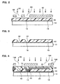
- Figs. 2 to 12 are views illustrating a semiconductor device manufacturing method according to this embodiment.
- interconnects 20, external terminals 30 and a plurality of resin layers are formed on an aggregate 10.
- the aggregate 10 has multiple semiconductor elements 12.
- the aggregate 10 may be a silicon wafer.
- a plurality of electrodes 14 are formed on each of the semiconductor elements 12.
- a semiconductor device is obtained by cutting apart the semiconductor devices shown in Fig. 1.
- This semiconductor device 1 includes a semiconductor element (semiconductor chip) 12, interconnects 20, external terminals 30, and a plurality of resin layers (in Fig. 1, a first resin layer 40 and a second resin layer 100). At least one of the plurality of resin layers (in Fig. 1, both of the resin layers) is formed avoiding the edges of the semiconductor element 12. Because the package size of the semiconductor device 1 is substantially the same as the size of the semiconductor chip, it can be classified as a CSP, or can be the to be a flip chip having a stress-moderating function.
- the plurality of electrodes 14 are formed on one surface (the active surface) of the semiconductor element 12.
- the plurality of electrodes 14 are formed along at least one side (including two opposite sides or all the sides). Or, the electrodes 14 may be formed in the middle of one surface of the semiconductor element 12.
- a passivation film 16 of SiN, SiO 2 , MgO or the like is formed on the semiconductor element 12, avoiding the electrodes 14.
- the passivation film 16 is an electrically insulating film.
- the passivation film 16, unlike the plurality of resin layers in this embodiment, may be made of a material other than resin.
- the passivation film 16 may be formed over the entire surface of the semiconductor element 12, avoiding the electrodes 14 at least partly.
- An interconnect 20 is electrically connected to each of the electrodes 14 on the surface of the semiconductor element 12 on which the electrodes 14 are formed.
- the interconnect 20 is often made up of a plurality of layers.
- the interconnect 20 can be formed by layering any of copper (Cu), chrome (Cr), titanium (Ti) , nickel (Ni), titanium tungsten (TiW), gold (Au), aluminum (Al), nickel vanadium (NiV), and tungsten (W).
- the electrodes 14 are formed at the edges of the semiconductor element 12, the interconnects 20 are led toward the center of the semiconductor element 12.
- an interconnect pattern is formed on the surface of the semiconductor element 12.
- an external terminal 30 is formed on each of the interconnects 20, avoiding the position directly above the electrode 14.
- the external terminal 30 is formed on for example a land section 22 of the interconnect 20.
- the land section 22 is formed with a larger area than the part led out from the electrode 14 (the line). Because the external terminal 30 is formed avoiding the position directly above the electrode 14, stresses acting on the external terminal 30 do not act directly on the electrode 14.
- the external terminal 30 is for example a solder ball, and is used for electrically connecting the semiconductor device to a circuit board.
- the first resin layer 40 may be formed in a plurality of layers, but in the example shown in Fig. 1 it is formed in one layer.
- the first resin layer 40 may have a stress-moderating function.
- the first resin layer 40 can be formed from polyimide resin, silicone-modified polyimide resin, epoxy resin, silicone-modified epoxy resin, benzocyclobutene (BCB), polybenzoxazole (PBO) or the like.
- the first resin layer 40 is formed over a region including the area below the interconnect 20. Specifically, the first resin layer 40 is formed on the aggregate 10, and the land section 22 and the line connected thereto are formed on the first resin layer 40. In other words, the first resin layer 40 is formed at least between the interconnect 20 and the semiconductor element 12.
- the second resin layer 100 is formed in one layer or a plurality of layers.
- the second resin layer 100 is formed over a region including the area above the interconnect 20.
- the second resin layer 100 may be made of the same material as the first resin layer 40, and at least one layer of it may have a stress-moderating function. Or, the second resin layer 100 may be made of a material different from that of the first resin layer 40.
- the second resin layer 100 includes an uppermost layer 60 and a lowermost layer 50.
- the uppermost layer 60 and the lowermost layer 50 may be made of different materials.
- As the material of the uppermost layer 60 preferably a material which can be used for the above-mentioned first resin layer 40 is used, and it is particularly desirable to use a material having a lower Young's modulus than the material of the first resin layer 40 and the other layers constituting the second resin layer 100 (the lowermost layer 50).
- the interconnect 20 is connected at one part to the electrode 14 and from there is led to reach a position above the first resin layer 40.
- the land section 22 is formed on the first resin layer 40.
- the first resin layer 40 is formed on the aggregate 10, exposing the electrode 14. Specifically, the first resin layer 40 is formed on the passivation film 16 of the aggregate 10.
- the lowermost layer 50 is for example solder resist and is formed so as to cover the interconnect 20. In this case, the lowermost layer 50 is formed avoiding the land section 22 of the interconnect 20. The lowermost layer 50 may also be formed on the first resin layer 40.
- the uppermost layer 60 may be formed so as to cover the interconnect 20 instead of the lowermost layer 50.
- the uppermost layer 60 is formed around the bottom of the external terminal 30.
- the uppermost layer 60 may be formed so as to cover the sides of the external terminal 30, except a top portion of the external terminal 30. In either case, as a result of part of the uppermost layer 60 being removed, at least a top portion of the external terminal 30 is exposed.
- the thermal expansion coefficient of the second resin layer 100 may be larger than that of the first resin layer 40. By this means, it is possible to relieve thermal stresses acting on the external terminal 30.
- the first resin layer 40 is formed to be disposed within an outline of the semiconductor element 12. Specifically, the first resin layer 40 is formed avoiding the edges of the semiconductor element 12. In this case, as shown in Fig. 1, the second resin layer 100 may also be formed avoiding the edges of the semiconductor element 12.
- the edge surfaces of the first resin layer 40 and the second resin layer 100 of the semiconductor device 1 may be edges formed by an exposure technique, a printing method or an ink jet method or the like. These edge surfaces may be smooth edge surfaces different from mechanically cut edge surfaces or, as shown in Fig. 1, may be sloping surfaces forming a taper so that each of the resin layers becomes smaller as the distance from the semiconductor element 12 becomes larger.
- the second resin layer 100 may be formed so as to cover the edges of the semiconductor element 12. That is, the cut surfaces of the second resin layer 100 may be positioned at the edges of the semiconductor device 1. In this case, just the uppermost layer 60 of the second resin layer 100 may be formed so as to cover the edges of the semiconductor element 12.
- the uppermost layer 60 is made using a material having a lower Young's modulus than the other resin layers (the first resin layer 40 and the lowermost layer 50 of the second resin layer 100), it is possible to reduce cracking of the semiconductor element 12 in the cutting region 70, reduce the progress of any cracking, and prevent detachment of the first resin layer 40 and the second resin layer 100 from the semiconductor element 12. Also, because the uppermost layer 60 does not have to be provided avoiding the edges of the semiconductor element 12, the semiconductor device can be manufactured by a simple process.
- At least one resin layer among a plurality of resin layers (for example at least a first resin layer 40) is formed avoiding a cutting region 70.
- an aggregate 10 (see Fig. 8) having multiple electrodes 14 and having formed thereon a passivation film 16 avoiding the electrodes 14 at least partly is prepared.
- the first resin layer 40 for forming interconnects 20 on is formed.
- the first resin layer 40 may be formed by an exposure technique.
- the first resin layer 40 is provided over the entire surface of the aggregate 10 (specifically, the passivation film 16) and the electrodes 14.
- a resin whose properties change in response to energy such as photopolymer, can be used, and it may be either one whose solubility increases (positive type) or one whose solubility decreases (negative type) when it is irradiated with energy.
- holes 44 for exposing the electrodes 14 are formed, and an opening 42 is formed in the cutting region 70.
- the hole 44 is formed over each of the electrodes 14.
- the opening 42 is formed continuously along the cutting region 70 of the aggregate 10. In other words, the opening 42 is formed along the boundary lines between the adjacent semiconductor elements 12 of the aggregate 10.
- a mask 80 with openings 82, 84 formed therein is disposed above the first resin layer 40 and energy 90 is radiated onto the first resin layer 40 through the mask 80.
- the openings 82, 84 are disposed over the regions where the opening 42 and the holes 44 are to be formed.
- the material of the first resin layer 40 is one whose solubility decreases when it is irradiated with energy, the regions where the opening 42 and the holes 44 are to be formed are covered and openings are disposed over the other regions.
- the opening 42 is formed below the opening 82 and the holes 44 exposing the electrodes 14 are formed below the openings 84.
- this kind of energy irradiation technique (light exposure technique or the like) is applied, because energy gets around the openings 82, 84 of the mask 80, the opening edges of the opening 42 and the holes 44 are formed with curved surfaces.
- an interconnect 20 is formed from each of the electrodes 14 on the first resin layer 40.
- the interconnect 20 may be formed by photolithography, sputtering or plating or the like.
- a land section 22 is formed as part of the interconnect 20
- the land section 22 is formed on the first resin layer 40.
- the interconnect 20 is formed also on the side surfaces of the holes 44 in the first resin layer 40.
- an external terminal 30 By the interconnect 20 being led out from the electrode 14, it is possible for an external terminal 30 to be formed avoiding the position directly above the electrode 14. And, by this means, the external terminal 30 can be provided within the active region of the semiconductor element 12. That is, pitch conversion is possible. Accordingly, in the disposition of the external terminal 30, the inside of the active region, i.e. a region constituting a fixed surface, can be provided, and the freedom of the set position of the external terminal 30 increases. For example by making the interconnects 20 curve at required positions, external terminals 30 can be lined up in the form of a grid.
- a lowermost layer 50 is formed.
- the lowermost layer 50 is provided over the entire surface of the first resin layer 40 and the interconnect 20.
- the opening 42 formed in the first resin layer 40 is also filled with the material of the lowermost layer 50. This step is preferably carried out after the first resin layer 40 is hardened.
- an opening 52 is formed in the lowermost layer 50.
- This may be carried out by the same method as the process used for the first resin layer 40.
- a mask 180 having openings 182, 184 formed therein is disposed above the lowermost layer 50 and energy is radiated onto the lowermost layer 50 through the mask 180.
- the openings 182, 184 are disposed above the regions where the opening 52 and a hole 54 are to be formed.
- a material whose solubility decreases when it is irradiated with energy may be used as the material of the lowermost layer 50.
- the part of the lowermost layer 50 within the opening 42 is removed and the opening 52 is formed.
- the hole 54 exposing a part (the land section 22) of the interconnect 20 is formed.
- a external terminal 30 can be provided simply in a later step.
- the step of forming the lowermost layer 50 may be omitted and an uppermost layer 60, discussed below, formed on the interconnects 20 instead.
- external terminals 30 and the uppermost layer 60 are formed.
- Each of the external terminals 30 is formed on the interconnect 20.
- the external terminal 30 is formed on a part (the land section 22) of the interconnect 20 formed on the first resin layer 40.
- the external terminal 30 is provided on a part (the land section 22) of the interconnect 20 exposed by the lowermost layer 50.
- the external terminal 30 can be provided easily.
- the external terminal 30 may be formed by providing a solder ball on the land section 22. Or, solder cream may be provided on the land section 22 and this then melted and made into a ball by surface tension.
- the uppermost layer 60 is formed.
- the uppermost layer 60 is formed so that at least a top portion of the external terminal 30 is exposed.
- the uppermost layer 60 may be provided at least around the bottom of the external terminal 30.
- the uppermost layer 60 made from a non-light-sensitive resin is provided over the entire surface of the lowermost layer 50 and the external terminal 30.
- the openings 42, 52 are also filled with the material of the uppermost layer 60.
- part of the uppermost layer 60 is physically removed to expose at least a top portion of the external terminal 30.
- the parts within the openings 42, 52 are removed, and an opening 62 is further formed.
- the openings 42, 52 and 62 are connected vertically and the cutting region 70 can be avoided.
- the openings 52 and 62 in the lowermost layer 50 and the uppermost layer 60 are formed separately, but alternatively these openings for avoiding the cutting region 70 may be formed at a time after the lowermost layer 50 and the uppermost layer 60 are both formed.
- the uppermost layer 60 may be formed only around the bottom of the external terminal 30. That is, the cutting region 70 may be avoided by causing the openings 42, 52 to connect in the vertical direction.
- the uppermost layer 60 may be formed using an exposure technique, in the same way as the first resin layer 40.
- both the first resin layer 40 and the second resin layer 100 were formed avoiding the cutting region 70
- the present embodiment is not limited to this. That is, when the Young's modulus of the material of the lowermost layer 50 and the uppermost layer 60 constituting the second resin layer 100 is lower than that of the first resin layer 40, the lowermost layer 50 and the uppermost layer 60 maybe formed so as to cover the cutting region 70. In particular, it is desirable for only the uppermost layer 60, which supports the bottom of the external terminal 30, to be provided so as to cover the cutting region 70 (see second embodiment).
- the material of the second resin layer 100 covering the cutting region 70 is a material having a lower Young's modulus than the material of the first resin layer 40 and the other layers constituting the second resin layer 100 (the lowermost layer 50)
- the occurrence of cracking of the edges of the semiconductor element 12 arising when the aggregate 10 is diced, and its progress, can be reduced, and detachment of the first resin layer 40 and the second resin layer 100 from the semiconductor element 12 can be reduced.
- the aggregate 10 is diced along the cutting region 70. That is, the aggregate of semiconductor devices including the aggregate 10 of multiple semiconductor elements 12 is diced to form a semiconductor device 1 for each of the semiconductor elements 12.
- Fig. 7 is a view showing a cross-section of the aggregate 10 being cut
- Fig. 8 is a view showing the aggregate 10 as a whole being cut.
- the aggregate 10 is cut from the side on which the electrodes 14 are formed.
- a blade 110 is positioned on the cutting region 70, which at least the first resin layer 40 is formed to avoid.
- the aggregate 10 can then be cut by the blade 110 being rotated at high speed.
- the aggregate 10 may be affixed to tape (not shown) for cutting.
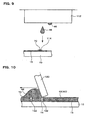
- At least one resin layer (for example at least the first resin layer 40) formed avoiding the cutting region 70 is formed by an ink jet method.
- the ink jet method by applying technology used in ink jet printers, the ink can be rapidly and economically provided without wasting.
- the ink jet head 112 shown in Fig. 9 is for example one used in an ink jet printer, and either a piezo jet type using a piezoelectric device or a bubble jet type using an electro-thermal convertor as an energy-generating device can be used. By this means it is possible to set freely the discharge area and discharge pattern of a paste 46 to become the first resin layer 40.
- a material 114 having a constituent which repels the paste 46 of the first resin layer 40 may be provided on the cutting region 70 for the formation of the first resin layer 40.
- the material 114 may for example be a fluorine-based compound.
- At least one resin layer (for example at least the first resin layer 40) formed avoiding the cutting region 70 is formed by a printing method.
- the first resin layer 40 is provided avoiding the electrodes 14.
- the cutting region 70 and the electrodes 14 are covered with a mask 122.
- the paste 46 to be the material of the first resin layer 40 is provided over the entire surface of the aggregate 10, and the paste 46 is spread uniformly to the height of the mask 122 in the open regions of the mask 122.
- a squeegee 120 can be used to spread the paste 46 over the openings.
- the mask 122 is removed to leave a first resin layer 40 formed in the regions where it is necessary, avoiding the cutting region 70 and the electrodes 14.
- At least one resin layer (for example at least the first resin layer 40) is formed in a region avoiding the cutting region 70 by first being formed on a separate member 130 by patterning and then transferred to the aggregate 10.
- the first resin layer 40 is provided avoiding the electrodes 14.
- the first resin layer 40 may be excluded by providing the material 114. By this means it is possible to form the first resin layer 40 avoiding the cutting region 70 with certainty.
- Fig. 12 is a view showing the vicinity of the external terminal 30 of this variation.
- This variation is a variation of the semiconductor device of the embodiment.
- the form of the part of a second resin layer 102 including an uppermost layer 160 provided around the external terminal 30 differs from that described above.
- the diameter D 2 of the contact section of the external terminal 30 connected to the land section 22 and the diameter D of the external terminal 30 are in the relationship: D 2 ⁇ D
- the uppermost layer 160 is formed so that the diameter D 2 of the contact section and the diameter D 1 of the part of the external terminal 30 exposed from the uppermost layer 160 have the relationship: D 1 ⁇ D 2 That is, within a limit such that the electrical connection between the external terminal 30 and the circuit board is not impaired, the uppermost layer 160 can be formed covering the outside of the external terminal 30. In this case, as shown in Fig. 12, the part of the uppermost layer 160 covering the external terminal 30 may protrude above the rest of the uppermost layer 160.
- Figs. 13 to 15 are views illustrating a semiconductor device and manufacturing method thereof according to this embodiment.
- Fig. 13 is a sectional view of an aggregate (semiconductor wafer) including semiconductor devices according to this embodiment.
- Fig. 14 is a plan view of a semiconductor device according to this embodiment, and specifically is a plan view of a semiconductor chip obtained by dicing the aggregate shown in Fig. 13. In Fig. 14, interconnects 220 and a second resin layer 104 are omitted.
- Fig. 15 is a sectional view of an aggregate (semiconductor wafer) including a semiconductor device according to a variation of this embodiment.
- a semiconductor device includes an individual semiconductor element (semiconductor chip) 12, interconnects 220, external terminals 30 and a plurality of resin layers (in Fig. 13, a first resin layer 240 and a second resin layer 104). At least one of the plurality of resin layers (in Fig. 13, all of the resin layers) is formed avoiding the edges of the semiconductor element 12.
- the form of the first resin layer 240 differs from that in the first embodiment.
- the second resin layer 104 may be formed in a single layer, in the example shown in Fig. 13 it is made up of a plurality of layers, an uppermost layer 60 and a lowermost layer 250.
- the semiconductor device 2 is obtained by cutting apart the semiconductor devices shown in Fig. 13. Except for the following description, this semiconductor device may have the same form as in the first embodiment.
- the electrodes 14 are formed at the edges.
- the first resin layer 240 is formed in the middle of the semiconductor element 12.
- the first resin layer 240 is formed in a region on the semiconductor element 12 on the inner side of the electrodes 14.
- the first resin layer 240 is formed in the region sandwiched between the electrodes 14 lined up at the sides.
- the first resin layer 240 is formed in the region surrounded by the electrodes 14 lined up along the sides.
- the first resin layer 240 formed on the semiconductor element 12 may be integrated in one region, as shown in Fig. 14, or may be divided into a plurality of regions.
- the interconnects 220 can be formed on the first resin layer 240 from the electrodes 14 in the same way as in the first embodiment.
- the thermal expansion coefficient of the first resin layer 240 may be smaller than that of the second resin layer 104. By this means, it is possible to relieve thermal stresses acting on the external terminal 30.
- the second resin layer 104 is formed to be positioned within an outline of the semiconductor element 12. Specifically, the second resin layer 104 is formed avoiding the edges of the semiconductor element 12. Otherwise it may be the same as in the first embodiment.
- the uppermost layer 160 of the second resin layer 104 may be formed so as to cover the edges of the semiconductor element 12.
- the uppermost layer 60 is made of a material having a lower Young's modulus than the material of the first resin layer 240 and the other layers consisting of the second resin layer 104 (the lowermost layer 250). That is, of the plurality of resin layers, even if the uppermost layer 60 of the second resin layer 104 is formed reaching the edges of the semiconductor element 12, it is possible to effectively prevent cracking of the edges of the semiconductor element 12, reduce the progress of any such cracking, and prevent the resin layers from detaching from the edges of the semiconductor element 12.
- the first resin layer 240 is provided over the entire surface of the aggregate 10, including the electrodes 14, an exposure technique or the like is applied to form the first resin layer 240 into regions inside the electrodes 14 on each semiconductor element 12. By this means it is possible to form a first resin layer 240 avoiding the cutting region 70.
- the interconnects 220 are formed from the electrodes 14 on the first resin layer 240 and as necessary a lowermost layer 250 is formed. By forming holes 254 in the lowermost layer 250 exposing land sections 222 of the interconnects 220, it is possible to provide external terminals 30 easily. The step of forming the lowermost layer 250 may be omitted.
- the external terminals 30 and the uppermost layer 60 are formed in the same way as in the first embodiment, and openings 252, 62 are formed in the cutting region 70. Then, the aggregate 10 is cut up along the cutting region 70. By this means it is possible to reduce detachment of the plural resin layers of the semiconductor device.
- the uppermost layer 60 may be provided over the entire surface of the aggregate 10. That is, only the parts of the uppermost layer 60 covering the external terminals 30 may be removed. That is, the uppermost layer 60 may be left covering the cutting region 70 of the aggregate 10. By this means it is possible to form the uppermost layer 60 with a simple process.
- the first to fourth variations of the embodiment described above can be applied to the manufacture of the semiconductor device.
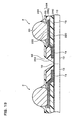
- Figs. 16 to 18 are views illustrating a semiconductor device and manufacturing method thereof according to this embodiment.
- Fig. 16 is a sectional view of an aggregate (semiconductor wafer) including semiconductor devices according to this embodiment.
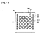
- Fig. 17 is a plan view of a semiconductor device according to this embodiment, and specifically a plan view of a semiconductor chip obtained by dicing the aggregate shown in Fig. 16.
- interconnects 220 and the second resin layer 104 are omitted.
- Fig. 18 is a sectional view of an aggregate (semiconductor wafer) including semiconductor devices according to a variation of this embodiment.
- a semiconductor device includes an individual semiconductor element (semiconductor chip) 12, interconnects 220, external terminals 30 and a plurality of resin layers (in Fig. 16, a first resin layer 340 and a second resin layer 104). At least one of the plurality of resin layers (in Fig. 16, all of the resin layers) is formed avoiding the edges of the semiconductor element 12.
- the form of a first resin layer 340 differs from that in the first embodiment.
- the semiconductor device 3 is illustrated by cutting apart the semiconductor devices as shown in Fig. 16. Except for the following description, this semiconductor device may have the same form as in the first and second embodiments.
- the first resin layer 340 of this embodiment is formed only below the external terminals 30. Any first resin layer 340 is formed below each of the external terminals 30 formed on the semiconductor element 12. That is, the first resin layers 340 are so formed that they are the same in number as the number of external terminals 30.
- each first resin layer 340 in plane view of the semiconductor element 12 is formed larger than the outline of the external terminal 30.
- the outline of the first resin layer 340 may be circular or rectangular or the like.
- the uppermost layer 60 of the second resin layer 104 may be formed so as to cover the edges of the semiconductor element 12.
- the uppermost layer 60 is made of a material having a lower Young's modulus than the material of the first resin layer 340 and the other layers consisting of the second resin layer 104 (the lowermost layer 250). That is, of the plurality of resin layers, even if the uppermost layer 60 of the second resin layer 104 is formed reaching the edges of the semiconductor element 12, it is possible to effectively prevent cracking of the edges of the semiconductor element 12, reduce the progress of any such cracking, and prevent the resin layers from detaching from the edges of the semiconductor element 12.
- This semiconductor device can be manufactured by using the same method as in the second embodiment to form the first resin layers 340 only below the external terminals 30.
- the first to fourth variations of the embodiment described above can be applied to the manufacture of the semiconductor device.
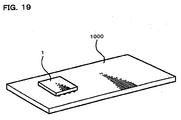
- Fig. 19 shows a circuit board 1000 on which is mounted a semiconductor device 1 according to the embodiments described above.
- a semiconductor device 1 for example an organic substrate such as a glass epoxy board is generally used for the circuit board 1000.
- interconnect patterns made of copper are formed on the circuit board 1000 so as to constitute a desired circuit, and these interconnect patterns are mechanically connected to the external terminals 30 of the semiconductor device 1 to achieve electrical continuity between the two.
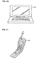
- a notebook computer 1100 is shown in Fig. 20 and a mobile telephone 1200 is shown in Fig. 21.
Landscapes
- Internal Circuitry In Semiconductor Integrated Circuit Devices (AREA)
- Encapsulation Of And Coatings For Semiconductor Or Solid State Devices (AREA)
- Production Of Multi-Layered Print Wiring Board (AREA)
- Structures Or Materials For Encapsulating Or Coating Semiconductor Devices Or Solid State Devices (AREA)
Abstract
Description
the second resin layer may be formed of a plurality of layers;
the lowermost layer in the second resin layer may be formed avoiding part of the interconnect in which the external terminal is formed, in the step of forming the resin layers; and
the external terminal may be formed on part of the interconnect exposed from the second resin layer, in the step of forming the external terminal. The external terminal can be thus formed more simply.
each of the semiconductor elements may be provided with a plurality of electrodes; and
the first resin layer may be formed on each of the semiconductor elements on the inside of the electrodes, in the step of forming the resin layers. The first resin layer can be thus provide avoiding the cutting region. Moreover, by reducing the area of the first resin layer, the stress applied to the external terminal can be effectively relieved even when the thermal expansion coefficients of the semiconductor element and the first resin layer differ to some extent.
the semiconductor chip may have a plurality of electrodes; and
the at least one resin layer may be formed on the semiconductor chip on the inside of the electrodes. Since the area of the resin layer is small, the stress applied to the external terminal can be effectively relieved even when the thermal expansion coefficients of the semiconductor chip and the resin layer differ to some extent.
the plurality of resin layers may include a resin layer provided on the interconnect to cover a bottom periphery of the external terminal; and
part of the external terminal exposed from the resin layer may be smaller than another part of the external terminal connected to the interconnect. By increasing a contact area between the resin layer and the external terminal, the stress can be further effectively relieved.
Claims (21)
- A method of manufacturing a semiconductor device, comprising the steps of:wherein at least one resin layer among the plurality of resin layers is formed avoiding a cutting region of the aggregate.forming a plurality of resin layers, an interconnect electrically connected to an electrode of each of a plurality of semiconductor elements, and an external terminal electrically connected to the interconnect, on an aggregate of semiconductor elements having an electrode; andcutting the aggregate,
- The method of manufacturing a semiconductor device as defined in claim 1,
wherein the at least one resin layer is formed by an ink jet method or a printing method. - The method of manufacturing a semiconductor device as defined in claim 1,
wherein the at least one resin layer is formed by transferring a previously-formed pattern to the aggregate. - The method of manufacturing a semiconductor device as defined in any one of claims 1 to 3,
wherein a material having a component which repels the at least one resin layer is provided to the cutting region of the aggregate in order to form the at least one resin layer by repelling. - The method of manufacturing a semiconductor device as defined in claim 1,
wherein the at least one resin layer is formed of a light-sensitive material; and
wherein the at least one resin layer is formed by removing part of the at least one resin layer disposed over the cutting region of the aggregate, by exposure. - The method of manufacturing a semiconductor device as defined in any one of claims 1, 2, 3 and 5,
wherein the plurality of resin layers include a first resin layer below the interconnect and a second resin layer above the interconnect; and
wherein at least the first resin layer is formed avoiding the cutting region of the aggregate, in the step of forming the resin layers. - The method of manufacturing a semiconductor device as defined in claim 6,
wherein the second resin layer is formed avoiding the cutting region of the aggregate, in the step of forming the resin layers. - The method of manufacturing a semiconductor device as defined in claim 7,
wherein at least an uppermost layer in the second resin layer is provided to cover the external terminal and the cutting region of the aggregate; and
wherein part of the uppermost layer disposed over the cutting region of the aggregate is removed to expose at least a top portion of the external terminal, in the step of forming the resin layers. - The method of manufacturing a semiconductor device as defined in claim 6,
wherein the second resin layer is formed of a plurality of layers; and
wherein at least the uppermost layer in the second resin layer is formed to cover the cutting region of the aggregate, in the step of forming the resin layers. - The method of manufacturing a semiconductor device as defined in any one of claims 1, 2, 3 and 5,
wherein the plurality of resin layers include a first resin layer below the interconnect and a second resin layer above the interconnect; and
wherein at least the second resin layer is formed avoiding the cutting region of the aggregate, in the step of forming the resin layers. - The method of manufacturing a semiconductor device as defined in claim 6,
wherein the thermal expansion coefficient of the second resin layer is larger than the thermal expansion coefficient of the first resin layer. - The method of manufacturing a semiconductor device as defined in claim 6,
wherein the second resin layer is formed such that part of the external terminal exposed from the second resin layer is smaller than a contact portion of the external terminal connected to the interconnect, in the step of forming the resin layers. - The method of manufacturing a semiconductor device as defined in claim 6,
wherein the second resin layer is formed of a plurality of layers;
wherein the lowermost layer in the second resin layer is formed avoiding part of the interconnect in which the external terminal is formed, in the step of forming the resin layers; and
wherein the external terminal is formed on part of the interconnect exposed from the second resin layer, in the step of forming the external terminal. - The method of manufacturing a semiconductor device as defined in claim 6,
wherein each of the semiconductor elements is provided with a plurality of electrodes; and
wherein the first resin layer is formed on each of the semiconductor elements on the inside of the electrodes, in the step of forming the resin layers. - A semiconductor device manufactured by the method as defined in any one of claims 1, 2, 3 and 5.
- A semiconductor device comprising:wherein at least one resin layer among the plurality of the resin layers is disposed within an outline of the semiconductor chip.a semiconductor chip having an electrode;an interconnect electrically connected to the electrode of the semiconductor chip;an external terminal electrically connected to the interconnect; anda plurality of resin layers provided on a surface of the semiconductor chip on which the electrode is formed,
- The semiconductor device as defined in claim 16, wherein the at least one resin layer is formed below the interconnect.
- The semiconductor device as defined in claim 16,
wherein the semiconductor chip has a plurality of electrodes; and
wherein the at least one resin layer is formed on the semiconductor chip on the inside of the electrodes. - The semiconductor device as defined in any one of claims 16 to 18,
wherein the plurality of resin layers include a resin layer provided on the interconnect to cover a bottom periphery of the external terminal; and
wherein part of the external terminal exposed from the resin layer is smaller than another part of the external terminal connected to the interconnect. - A circuit board over which is mounted the semiconductor device as defined in any one of claims 16 to 18.
- Electronic equipment comprising the semiconductor device as defined in any one of claims 16 to 18.
Applications Claiming Priority (3)
| Application Number | Priority Date | Filing Date | Title |
|---|---|---|---|
| JP2000081999 | 2000-03-23 | ||
| JP2000081999 | 2000-03-23 | ||
| PCT/JP2001/002325 WO2001071805A1 (en) | 2000-03-23 | 2001-03-23 | Semiconductor device, method of manufacture thereof, circuit board, and electronic device |
Publications (3)
| Publication Number | Publication Date |
|---|---|
| EP1198003A1 true EP1198003A1 (en) | 2002-04-17 |
| EP1198003A4 EP1198003A4 (en) | 2005-12-14 |
| EP1198003B1 EP1198003B1 (en) | 2013-08-28 |
Family
ID=18598853
Family Applications (1)
| Application Number | Title | Priority Date | Filing Date |
|---|---|---|---|
| EP01915722.1A Expired - Lifetime EP1198003B1 (en) | 2000-03-23 | 2001-03-23 | Method of manufacturing a semiconductor device and electronic device |
Country Status (6)
| Country | Link |
|---|---|
| US (1) | US6707153B2 (en) |
| EP (1) | EP1198003B1 (en) |
| KR (1) | KR100440507B1 (en) |
| CN (1) | CN1311547C (en) |
| TW (1) | TW515064B (en) |
| WO (1) | WO2001071805A1 (en) |
Cited By (6)
| Publication number | Priority date | Publication date | Assignee | Title |
|---|---|---|---|---|
| US7129581B2 (en) | 2003-12-17 | 2006-10-31 | Seiko Epson Corporation | Semiconductor device, method of manufacturing thereof, circuit board and electronic apparatus |
| US7615864B2 (en) | 2003-12-17 | 2009-11-10 | Seiko Epson Corporation | Semiconductor device, method of manufacturing thereof, circuit board and electronic apparatus |
| US7679153B2 (en) | 2004-09-13 | 2010-03-16 | Seiko Epson Corporation | Sealed surface acoustic wave element package |
| GB2464549A (en) * | 2008-10-22 | 2010-04-28 | Cambridge Silicon Radio Ltd | Wafer Level Chip Scale Packaging |
| EP2873091A4 (en) * | 2012-07-16 | 2016-03-30 | Micron Technology Inc | PILLAR ON PLATE INTERCONNECTION STRUCTURES, SEMICONDUCTOR CHIPS, AND CHIP ASSEMBLY COMPRISING SUCH INTERCONNECT STRUCTURES AND ASSOCIATED METHODS |
| EP3211661A3 (en) * | 2016-02-26 | 2017-09-13 | Shin-Etsu Chemical Co., Ltd. | Method for manufacturing a flip-chip type semiconductor apparatus using a photosensitive adhesive layer and corresponding flip-chip type semiconductor apparatus |
Families Citing this family (43)
| Publication number | Priority date | Publication date | Assignee | Title |
|---|---|---|---|---|
| US6563299B1 (en) * | 2000-08-30 | 2003-05-13 | Micron Technology, Inc. | Apparatus for measuring parasitic capacitance and inductance of I/O leads on an electrical component using a network analyzer |
| DE10256662A1 (en) * | 2002-12-04 | 2004-06-17 | Robert Bosch Gmbh | Fuel injector |
| JP3925283B2 (en) | 2002-04-16 | 2007-06-06 | セイコーエプソン株式会社 | Method for manufacturing electronic device, method for manufacturing electronic device |
| JP2004134709A (en) | 2002-10-15 | 2004-04-30 | Seiko Epson Corp | Semiconductor device and manufacturing method thereof, circuit board, and electronic apparatus |
| JP2004241696A (en) * | 2003-02-07 | 2004-08-26 | Seiko Epson Corp | Semiconductor device and its manufacturing method, circuit board, and electronic equipment |
| JP3945415B2 (en) | 2003-02-14 | 2007-07-18 | セイコーエプソン株式会社 | Manufacturing method of semiconductor device |
| JP3726906B2 (en) * | 2003-03-18 | 2005-12-14 | セイコーエプソン株式会社 | Semiconductor device and manufacturing method thereof, circuit board, and electronic apparatus |
| JP2004304152A (en) * | 2003-03-20 | 2004-10-28 | Seiko Epson Corp | Semiconductor wafer, semiconductor device and manufacturing method thereof, circuit board, and electronic apparatus |
| JP3918941B2 (en) * | 2003-03-20 | 2007-05-23 | セイコーエプソン株式会社 | Manufacturing method of semiconductor device |
| JP2004304151A (en) * | 2003-03-20 | 2004-10-28 | Seiko Epson Corp | Semiconductor wafer, semiconductor device and manufacturing method thereof, circuit board, and electronic apparatus |
| JP3666495B2 (en) * | 2003-06-27 | 2005-06-29 | セイコーエプソン株式会社 | Semiconductor device and manufacturing method thereof, circuit board, and electronic apparatus |
| TWI223884B (en) * | 2003-06-30 | 2004-11-11 | Advanced Semiconductor Eng | Under bump metallurgy structure |
| DE10335182B4 (en) * | 2003-07-30 | 2007-03-01 | Infineon Technologies Ag | Arrangement for improving the module reliability |
| TW592013B (en) * | 2003-09-09 | 2004-06-11 | Advanced Semiconductor Eng | Solder bump structure and the method for forming the same |
| JP3953027B2 (en) | 2003-12-12 | 2007-08-01 | ソニー株式会社 | Semiconductor device and manufacturing method thereof |
| JP3734039B2 (en) | 2004-03-15 | 2006-01-11 | セイコーエプソン株式会社 | Semiconductor device and manufacturing method thereof, circuit board, and electronic apparatus |
| TWI245431B (en) * | 2004-09-10 | 2005-12-11 | Advanced Semiconductor Eng | Package structure and method for optoelectric products |
| JP3841096B2 (en) * | 2004-09-28 | 2006-11-01 | セイコーエプソン株式会社 | Wiring pattern forming method, multilayer wiring board manufacturing method, electronic device |
| JP4016984B2 (en) * | 2004-12-21 | 2007-12-05 | セイコーエプソン株式会社 | Semiconductor device, semiconductor device manufacturing method, circuit board, and electronic device |
| JP4297106B2 (en) * | 2005-02-23 | 2009-07-15 | セイコーエプソン株式会社 | Film pattern forming method, device manufacturing method, electro-optical device, and electronic apparatus |
| JP4055015B2 (en) | 2005-04-04 | 2008-03-05 | セイコーエプソン株式会社 | Manufacturing method of semiconductor device |
| JP4311376B2 (en) | 2005-06-08 | 2009-08-12 | セイコーエプソン株式会社 | Semiconductor device, semiconductor device manufacturing method, electronic component, circuit board, and electronic apparatus |
| JP4265575B2 (en) * | 2005-06-21 | 2009-05-20 | セイコーエプソン株式会社 | Semiconductor chip and electronic equipment |
| JP4289335B2 (en) | 2005-08-10 | 2009-07-01 | セイコーエプソン株式会社 | Electronic components, circuit boards and electronic equipment |
| JP2007103717A (en) * | 2005-10-05 | 2007-04-19 | Sony Corp | Semiconductor device and manufacturing method thereof |
| JP2007115957A (en) * | 2005-10-21 | 2007-05-10 | Seiko Epson Corp | Semiconductor device and manufacturing method thereof |
| JP2007115958A (en) * | 2005-10-21 | 2007-05-10 | Seiko Epson Corp | Semiconductor device |
| KR100652443B1 (en) * | 2005-11-17 | 2006-12-01 | 삼성전자주식회사 | Wafer level package having a redistribution layer and a method of forming the same |
| JP4379413B2 (en) * | 2005-12-06 | 2009-12-09 | セイコーエプソン株式会社 | Electronic component, method for manufacturing electronic component, circuit board, and electronic device |
| KR100713931B1 (en) * | 2006-03-29 | 2007-05-07 | 주식회사 하이닉스반도체 | High speed and high performance semiconductor packages |
| US20080122078A1 (en) * | 2006-11-08 | 2008-05-29 | Jun He | Systems and methods to passivate on-die redistribution interconnects |
| JP4431901B2 (en) * | 2007-01-19 | 2010-03-17 | セイコーエプソン株式会社 | Semiconductor device |
| JP4273356B2 (en) * | 2007-02-21 | 2009-06-03 | セイコーエプソン株式会社 | Manufacturing method of semiconductor device |
| JP4305678B2 (en) | 2007-05-11 | 2009-07-29 | セイコーエプソン株式会社 | Semiconductor device |
| US8592312B2 (en) * | 2007-06-07 | 2013-11-26 | Globalfoundries Inc. | Method for depositing a conductive capping layer on metal lines |
| JP5139039B2 (en) * | 2007-11-20 | 2013-02-06 | 新光電気工業株式会社 | Semiconductor device and manufacturing method thereof |
| US9978656B2 (en) * | 2011-11-22 | 2018-05-22 | Taiwan Semiconductor Manufacturing Company, Ltd. | Mechanisms for forming fine-pitch copper bump structures |
| US10483132B2 (en) * | 2012-12-28 | 2019-11-19 | Taiwan Semiconductor Manufacturing Company, Ltd. | Post-passivation interconnect structure and method of forming the same |
| US20150311132A1 (en) * | 2014-04-28 | 2015-10-29 | Taiwan Semiconductor Manufacturing Company, Ltd. | Scribe line structure and method of forming same |
| CN110310938A (en) * | 2018-03-20 | 2019-10-08 | 中芯国际集成电路制造(上海)有限公司 | A kind of semiconductor devices and electronic device |
| KR102534733B1 (en) | 2018-07-31 | 2023-05-19 | 삼성전자 주식회사 | Fan-out semiconductor package having redistribution line structure |
| KR102571558B1 (en) | 2018-09-17 | 2023-08-29 | 삼성전자주식회사 | Semiconductor device |
| JP7081581B2 (en) * | 2019-12-23 | 2022-06-07 | Agc株式会社 | Cutting method, cutting device and laminate |
Family Cites Families (21)
| Publication number | Priority date | Publication date | Assignee | Title |
|---|---|---|---|---|
| JPS5893266A (en) * | 1981-11-30 | 1983-06-02 | Toshiba Corp | Semiconductor integrated circuit |
| US5470787A (en) * | 1994-05-02 | 1995-11-28 | Motorola, Inc. | Semiconductor device solder bump having intrinsic potential for forming an extended eutectic region and method for making and using the same |
| KR100367702B1 (en) * | 1995-03-20 | 2003-04-07 | 유나이티브 인터내셔널 리미티드 | Solder bump fabrication methods and structure including a titanium barrier layer |
| JPH08264489A (en) * | 1995-03-28 | 1996-10-11 | Nippon Precision Circuits Kk | Semiconductor device |
| KR100274333B1 (en) * | 1996-01-19 | 2001-01-15 | 모기 쥰이찌 | conductive layer adhesive anisotropic concuctive sheet and wiring board using such a sheet |
| TW448524B (en) * | 1997-01-17 | 2001-08-01 | Seiko Epson Corp | Electronic component, semiconductor device, manufacturing method therefor, circuit board and electronic equipment |
| KR100237328B1 (en) * | 1997-02-26 | 2000-01-15 | 김규현 | Structure of semiconductor package and manufacturing method |
| US6020637A (en) * | 1997-05-07 | 2000-02-01 | Signetics Kp Co., Ltd. | Ball grid array semiconductor package |
| JP3935558B2 (en) * | 1997-06-04 | 2007-06-27 | 大日本印刷株式会社 | Pattern formation method |
| JP3335575B2 (en) * | 1997-06-06 | 2002-10-21 | 松下電器産業株式会社 | Semiconductor device and manufacturing method thereof |
| US6441487B2 (en) * | 1997-10-20 | 2002-08-27 | Flip Chip Technologies, L.L.C. | Chip scale package using large ductile solder balls |
| US6097087A (en) * | 1997-10-31 | 2000-08-01 | Micron Technology, Inc. | Semiconductor package including flex circuit, interconnects and dense array external contacts |
| JP3618212B2 (en) * | 1998-01-08 | 2005-02-09 | 松下電器産業株式会社 | Semiconductor device and manufacturing method thereof |
| JPH11220069A (en) | 1998-02-02 | 1999-08-10 | Seiko Epson Corp | Semiconductor device and its manufacturing method, circuit board, and electronic equipment |
| US6333565B1 (en) * | 1998-03-23 | 2001-12-25 | Seiko Epson Corporation | Semiconductor device and method of manufacturing the same, circuit board, and electronic instrument |
| JP3538029B2 (en) * | 1998-06-09 | 2004-06-14 | 松下電器産業株式会社 | Method for manufacturing semiconductor device |
| JP2000040773A (en) * | 1998-07-23 | 2000-02-08 | Sony Corp | Resin-sealed semiconductor device and method of manufacturing the same |
| JP2000077563A (en) * | 1998-08-31 | 2000-03-14 | Sharp Corp | Semiconductor device and method of manufacturing the same |
| US6326701B1 (en) * | 1999-02-24 | 2001-12-04 | Sanyo Electric Co., Ltd. | Chip size package and manufacturing method thereof |
| US6388335B1 (en) * | 1999-12-14 | 2002-05-14 | Atmel Corporation | Integrated circuit package formed at a wafer level |
| KR100311975B1 (en) * | 1999-12-16 | 2001-10-17 | 윤종용 | semiconductor device and method for manufacturing the same |
-
2001
- 2001-03-23 US US09/814,802 patent/US6707153B2/en not_active Expired - Lifetime
- 2001-03-23 EP EP01915722.1A patent/EP1198003B1/en not_active Expired - Lifetime
- 2001-03-23 WO PCT/JP2001/002325 patent/WO2001071805A1/en not_active Ceased
- 2001-03-23 TW TW090106899A patent/TW515064B/en not_active IP Right Cessation
- 2001-03-23 KR KR10-2001-7014252A patent/KR100440507B1/en not_active Expired - Lifetime
- 2001-03-23 CN CNB01801366XA patent/CN1311547C/en not_active Expired - Lifetime
Cited By (16)
| Publication number | Priority date | Publication date | Assignee | Title |
|---|---|---|---|---|
| US8482121B2 (en) | 2003-12-17 | 2013-07-09 | Seiko Epson Corporation | Semiconductor device, method of manufacturing thereof, circuit board and electronic apparatus |
| US8847406B2 (en) | 2003-12-17 | 2014-09-30 | Seiko Epson Corporation | Semiconductor device, method of manufacturing thereof, circuit board and electronic apparatus |
| US9589886B2 (en) | 2003-12-17 | 2017-03-07 | Seiko Epson Corporation | Semiconductor device, method of manufacturing thereof, circuit board and electronic apparatus |
| US9105534B2 (en) | 2003-12-17 | 2015-08-11 | Seiko Epson Corporation | Semiconductor device, method of manufacturing thereof, circuit board and electronic apparatus |
| US7851265B2 (en) | 2003-12-17 | 2010-12-14 | Seiko Epson Corporation | Semiconductor device, method of manufacturing thereof, circuit board and electronic apparatus |
| US7982310B2 (en) | 2003-12-17 | 2011-07-19 | Seiko Epson Corporation | Semiconductor device, method of manufacturing thereof, circuit board and electronic apparatus |
| US7615864B2 (en) | 2003-12-17 | 2009-11-10 | Seiko Epson Corporation | Semiconductor device, method of manufacturing thereof, circuit board and electronic apparatus |
| US7129581B2 (en) | 2003-12-17 | 2006-10-31 | Seiko Epson Corporation | Semiconductor device, method of manufacturing thereof, circuit board and electronic apparatus |
| US8492856B2 (en) | 2004-09-13 | 2013-07-23 | Seiko Epson Corporation | Sealed electric element package |
| US8227878B2 (en) | 2004-09-13 | 2012-07-24 | Seiko Epson Corporation | Sealed surface acoustic wave element package |
| US7679153B2 (en) | 2004-09-13 | 2010-03-16 | Seiko Epson Corporation | Sealed surface acoustic wave element package |
| GB2464549B (en) * | 2008-10-22 | 2013-03-27 | Cambridge Silicon Radio Ltd | Improved wafer level chip scale packaging |
| GB2464549A (en) * | 2008-10-22 | 2010-04-28 | Cambridge Silicon Radio Ltd | Wafer Level Chip Scale Packaging |
| EP2873091A4 (en) * | 2012-07-16 | 2016-03-30 | Micron Technology Inc | PILLAR ON PLATE INTERCONNECTION STRUCTURES, SEMICONDUCTOR CHIPS, AND CHIP ASSEMBLY COMPRISING SUCH INTERCONNECT STRUCTURES AND ASSOCIATED METHODS |
| EP3211661A3 (en) * | 2016-02-26 | 2017-09-13 | Shin-Etsu Chemical Co., Ltd. | Method for manufacturing a flip-chip type semiconductor apparatus using a photosensitive adhesive layer and corresponding flip-chip type semiconductor apparatus |
| US10416557B2 (en) | 2016-02-26 | 2019-09-17 | Shin-Etsu Chemical Co., Ltd. | Method for manufacturing semiconductor apparatus, method for manufacturing flip-chip type semiconductor apparatus, semiconductor apparatus, and flip-chip type semiconductor apparatus |
Also Published As
| Publication number | Publication date |
|---|---|
| EP1198003B1 (en) | 2013-08-28 |
| CN1381070A (en) | 2002-11-20 |
| TW515064B (en) | 2002-12-21 |
| KR100440507B1 (en) | 2004-07-15 |
| US20020008320A1 (en) | 2002-01-24 |
| KR20020008181A (en) | 2002-01-29 |
| US6707153B2 (en) | 2004-03-16 |
| CN1311547C (en) | 2007-04-18 |
| EP1198003A4 (en) | 2005-12-14 |
| WO2001071805A1 (en) | 2001-09-27 |
Similar Documents
| Publication | Publication Date | Title |
|---|---|---|
| US6707153B2 (en) | Semiconductor chip with plural resin layers on a surface thereof and method of manufacturing same | |
| US7033935B2 (en) | Semiconductor device and method for manufacturing the same | |
| KR100306842B1 (en) | Redistributed Wafer Level Chip Size Package Having Concave Pattern In Bump Pad And Method For Manufacturing The Same | |
| US7417311B2 (en) | Semiconductor device and method of fabricating the same | |
| JP3846550B2 (en) | Semiconductor device and manufacturing method thereof, circuit board, and electronic apparatus | |
| US20060017161A1 (en) | Semiconductor package having protective layer for re-routing lines and method of manufacturing the same | |
| US7176572B2 (en) | Semiconductor wafer, semiconductor device and method of manufacturing the same, circuit board, and electronic equipment | |
| JP3804797B2 (en) | Semiconductor device and manufacturing method thereof | |
| US20070246826A1 (en) | Wafer level semiconductor module and method for manufacturing the same | |
| US20080203569A1 (en) | Semiconductor device and manufacturing method thereof | |
| KR20100093357A (en) | Wafer Level Chipscale Package | |
| JP2011134821A (en) | Semiconductor device, semiconductor wafer, and method of manufacturing semiconductor wafer | |
| JP4232044B2 (en) | Manufacturing method of semiconductor device | |
| US20070069320A1 (en) | Wiring structure of a semiconductor package and method of manufacturing the same, and wafer level package having the wiring structure and method of manufacturing the same | |
| JP3664707B2 (en) | Semiconductor device and manufacturing method thereof | |
| US7144760B2 (en) | Semiconductor device, method of manufacturing the same, circuit board, and electronic equipment | |
| JPWO2001071805A1 (en) | Semiconductor device and manufacturing method thereof, circuit board and electronic device | |
| US7602055B2 (en) | Semiconductor device and method for fabricating the same | |
| JP3726906B2 (en) | Semiconductor device and manufacturing method thereof, circuit board, and electronic apparatus | |
| JP3832558B2 (en) | Metal foil patterning method and wiring board manufacturing method | |
| JP2007095894A (en) | Semiconductor device and manufacturing method thereof | |
| KR20260036468A (en) | Substrate structure | |
| JP2006005219A (en) | Semiconductor device manufacturing method and semiconductor wafer |
Legal Events
| Date | Code | Title | Description |
|---|---|---|---|
| PUAI | Public reference made under article 153(3) epc to a published international application that has entered the european phase |
Free format text: ORIGINAL CODE: 0009012 |
|
| AK | Designated contracting states |
Kind code of ref document: A1 Designated state(s): AT BE CH CY DE DK ES FI FR GB GR IE IT LI LU MC NL PT SE TR |
|
| 17P | Request for examination filed |
Effective date: 20020306 |
|
| A4 | Supplementary search report drawn up and despatched |
Effective date: 20051031 |
|
| RIC1 | Information provided on ipc code assigned before grant |
Ipc: H01L 23/31 20060101ALI20121009BHEP Ipc: H01L 21/56 20060101AFI20121009BHEP |
|
| GRAJ | Information related to disapproval of communication of intention to grant by the applicant or resumption of examination proceedings by the epo deleted |
Free format text: ORIGINAL CODE: EPIDOSDIGR1 |
|
| GRAP | Despatch of communication of intention to grant a patent |
Free format text: ORIGINAL CODE: EPIDOSNIGR1 |
|
| REG | Reference to a national code |
Ref country code: DE Ref legal event code: R079 Ref document number: 60148278 Country of ref document: DE Free format text: PREVIOUS MAIN CLASS: H01L0023280000 Ipc: H01L0021560000 |
|
| GRAP | Despatch of communication of intention to grant a patent |
Free format text: ORIGINAL CODE: EPIDOSNIGR1 |
|
| RIC1 | Information provided on ipc code assigned before grant |
Ipc: H01L 21/56 20060101AFI20130410BHEP Ipc: H01L 23/31 20060101ALI20130410BHEP Ipc: H01L 21/78 20060101ALI20130410BHEP Ipc: H01L 23/00 20060101ALI20130410BHEP |
|
| INTG | Intention to grant announced |
Effective date: 20130422 |
|
| GRAS | Grant fee paid |
Free format text: ORIGINAL CODE: EPIDOSNIGR3 |
|
| GRAA | (expected) grant |
Free format text: ORIGINAL CODE: 0009210 |
|
| AK | Designated contracting states |
Kind code of ref document: B1 Designated state(s): AT BE CH CY DE DK ES FI FR GB GR IE IT LI LU MC NL PT SE TR |
|
| REG | Reference to a national code |
Ref country code: GB Ref legal event code: FG4D |
|
| REG | Reference to a national code |
Ref country code: CH Ref legal event code: EP |
|
| REG | Reference to a national code |
Ref country code: AT Ref legal event code: REF Ref document number: 629751 Country of ref document: AT Kind code of ref document: T Effective date: 20130915 |
|
| REG | Reference to a national code |
Ref country code: IE Ref legal event code: FG4D |
|
| REG | Reference to a national code |
Ref country code: DE Ref legal event code: R096 Ref document number: 60148278 Country of ref document: DE Effective date: 20131024 |
|
| REG | Reference to a national code |
Ref country code: AT Ref legal event code: MK05 Ref document number: 629751 Country of ref document: AT Kind code of ref document: T Effective date: 20130828 |
|
| REG | Reference to a national code |
Ref country code: NL Ref legal event code: VDEP Effective date: 20130828 |
|
| PG25 | Lapsed in a contracting state [announced via postgrant information from national office to epo] |
Ref country code: SE Free format text: LAPSE BECAUSE OF FAILURE TO SUBMIT A TRANSLATION OF THE DESCRIPTION OR TO PAY THE FEE WITHIN THE PRESCRIBED TIME-LIMIT Effective date: 20130828 Ref country code: CY Free format text: LAPSE BECAUSE OF NON-PAYMENT OF DUE FEES Effective date: 20130619 Ref country code: PT Free format text: LAPSE BECAUSE OF FAILURE TO SUBMIT A TRANSLATION OF THE DESCRIPTION OR TO PAY THE FEE WITHIN THE PRESCRIBED TIME-LIMIT Effective date: 20131230 Ref country code: AT Free format text: LAPSE BECAUSE OF FAILURE TO SUBMIT A TRANSLATION OF THE DESCRIPTION OR TO PAY THE FEE WITHIN THE PRESCRIBED TIME-LIMIT Effective date: 20130828 |
|
| REG | Reference to a national code |
Ref country code: NL Ref legal event code: VDEP Effective date: 20130828 |
|
| PG25 | Lapsed in a contracting state [announced via postgrant information from national office to epo] |
Ref country code: GR Free format text: LAPSE BECAUSE OF FAILURE TO SUBMIT A TRANSLATION OF THE DESCRIPTION OR TO PAY THE FEE WITHIN THE PRESCRIBED TIME-LIMIT Effective date: 20131129 Ref country code: BE Free format text: LAPSE BECAUSE OF FAILURE TO SUBMIT A TRANSLATION OF THE DESCRIPTION OR TO PAY THE FEE WITHIN THE PRESCRIBED TIME-LIMIT Effective date: 20130828 Ref country code: FI Free format text: LAPSE BECAUSE OF FAILURE TO SUBMIT A TRANSLATION OF THE DESCRIPTION OR TO PAY THE FEE WITHIN THE PRESCRIBED TIME-LIMIT Effective date: 20130828 |
|
| PG25 | Lapsed in a contracting state [announced via postgrant information from national office to epo] |
Ref country code: CY Free format text: LAPSE BECAUSE OF NON-PAYMENT OF DUE FEES Effective date: 20130828 |
|
| PG25 | Lapsed in a contracting state [announced via postgrant information from national office to epo] |
Ref country code: NL Free format text: LAPSE BECAUSE OF FAILURE TO SUBMIT A TRANSLATION OF THE DESCRIPTION OR TO PAY THE FEE WITHIN THE PRESCRIBED TIME-LIMIT Effective date: 20130828 Ref country code: DK Free format text: LAPSE BECAUSE OF FAILURE TO SUBMIT A TRANSLATION OF THE DESCRIPTION OR TO PAY THE FEE WITHIN THE PRESCRIBED TIME-LIMIT Effective date: 20130828 |
|
| PG25 | Lapsed in a contracting state [announced via postgrant information from national office to epo] |
Ref country code: IT Free format text: LAPSE BECAUSE OF FAILURE TO SUBMIT A TRANSLATION OF THE DESCRIPTION OR TO PAY THE FEE WITHIN THE PRESCRIBED TIME-LIMIT Effective date: 20130828 Ref country code: ES Free format text: LAPSE BECAUSE OF FAILURE TO SUBMIT A TRANSLATION OF THE DESCRIPTION OR TO PAY THE FEE WITHIN THE PRESCRIBED TIME-LIMIT Effective date: 20130828 |
|
| REG | Reference to a national code |
Ref country code: DE Ref legal event code: R097 Ref document number: 60148278 Country of ref document: DE |
|
| PLBE | No opposition filed within time limit |
Free format text: ORIGINAL CODE: 0009261 |
|
| STAA | Information on the status of an ep patent application or granted ep patent |
Free format text: STATUS: NO OPPOSITION FILED WITHIN TIME LIMIT |
|
| 26N | No opposition filed |
Effective date: 20140530 |
|
| REG | Reference to a national code |
Ref country code: DE Ref legal event code: R097 Ref document number: 60148278 Country of ref document: DE Effective date: 20140530 |
|
| PG25 | Lapsed in a contracting state [announced via postgrant information from national office to epo] |
Ref country code: LU Free format text: LAPSE BECAUSE OF FAILURE TO SUBMIT A TRANSLATION OF THE DESCRIPTION OR TO PAY THE FEE WITHIN THE PRESCRIBED TIME-LIMIT Effective date: 20140323 |
|
| REG | Reference to a national code |
Ref country code: CH Ref legal event code: PL |
|
| GBPC | Gb: european patent ceased through non-payment of renewal fee |
Effective date: 20140323 |
|
| REG | Reference to a national code |
Ref country code: FR Ref legal event code: ST Effective date: 20141128 |
|
| REG | Reference to a national code |
Ref country code: IE Ref legal event code: MM4A |
|
| PG25 | Lapsed in a contracting state [announced via postgrant information from national office to epo] |
Ref country code: GB Free format text: LAPSE BECAUSE OF NON-PAYMENT OF DUE FEES Effective date: 20140323 Ref country code: FR Free format text: LAPSE BECAUSE OF NON-PAYMENT OF DUE FEES Effective date: 20140331 Ref country code: CH Free format text: LAPSE BECAUSE OF NON-PAYMENT OF DUE FEES Effective date: 20140331 Ref country code: LI Free format text: LAPSE BECAUSE OF NON-PAYMENT OF DUE FEES Effective date: 20140331 Ref country code: IE Free format text: LAPSE BECAUSE OF NON-PAYMENT OF DUE FEES Effective date: 20140323 |
|
| PG25 | Lapsed in a contracting state [announced via postgrant information from national office to epo] |
Ref country code: MC Free format text: LAPSE BECAUSE OF FAILURE TO SUBMIT A TRANSLATION OF THE DESCRIPTION OR TO PAY THE FEE WITHIN THE PRESCRIBED TIME-LIMIT Effective date: 20130828 |
|
| PG25 | Lapsed in a contracting state [announced via postgrant information from national office to epo] |
Ref country code: TR Free format text: LAPSE BECAUSE OF FAILURE TO SUBMIT A TRANSLATION OF THE DESCRIPTION OR TO PAY THE FEE WITHIN THE PRESCRIBED TIME-LIMIT Effective date: 20130828 |
|
| PGFP | Annual fee paid to national office [announced via postgrant information from national office to epo] |
Ref country code: DE Payment date: 20200310 Year of fee payment: 20 |
|
| REG | Reference to a national code |
Ref country code: DE Ref legal event code: R071 Ref document number: 60148278 Country of ref document: DE |